
Projects Description
Brief description of the projects presented in the website.
Project 1
The first project in the website, a very simple 50-watt audio power amplifier. The project features differential input stage and paralleled power output transistors for handling low impedance 4Ω loads. Maximum recommended power supply is ±45VDC.
Project 2
Another simple circuit that features manual adjustment to the DC offset voltage. Another interesting change to the circuit is the very high value of the feedback resistor R17, twice that of Project1. The model unit uses 3 pairs of complementary power output transistors 2SC5200 and 2SA1943 or 2SC5242/2SA1962. The project is capable of providing 80 watts to an 8Ω load with ±45VDC power supply.
Project 3
Another simple 75-watt audio amplifier circuit but the audio quality is surprisingly good. The introduction of current source circuits improves the sonic quality of this project. The recommended power supply is ±35VDC.
Project 4
A classic audio amplifier circuit rated 70 watts at 8Ω with ±44VDC power supply rails. It uses two pairs of complementary power output transistors 2SC5242 and 2SA1962. An op-amp servo circuit controls the DC offset voltage of the amplifier. A few SMT components were combined with the rest of the thru-hole components to make it more challenging and enjoyable to build.
Project 5
The concept of this project originated from an application notes developed by Hitachi Semiconductor that features a classic 100-watt MOSFET audio power amplifier design. This project utilizes lateral power MOSFETS capable of providing 100 watts into an 8Ω load with a ±56VDC power supply rails.
Project 6
This project is rated at 230W into an 8Ω load with ±65VDC power supply rails. The input stage features differential amplifier, current-mirror and current-source circuits. A two-stage emitter-follower driver drives four pairs of full complementary emitter-follower power output stage transistors.
Project 7
The project delivers a power output of more than 130Watts into an 8Ω load using a power supply of ±56VDC. The improved circuit features manual adjustment to the DC offset voltage. The output stage is an emitter-follower configured similar to a T-circuit topology.
Project 8
A very popular project that features Texas Instruments’ LME49811, a high fidelity audio power amplifier input stage designed for pro-audio applications. The power amplifier produces 36.02Vrms across the 8Ω dummy load or a power output of 162 watts.
Project 9
This is a tone control project that uses Texas Instruments’ LM1036 Dual DC Operated Tone/Volume/Balance integrated circuit. Both LM1036 IC versions are presented in this project, a 20-pin through-hole Plastic Dual-Inline-Package (PDIP) and Small Outline Integrated Circuit (SOIC) surface mounted package.
Project 10
The project is rated at a continuous power output of 130 watts into 8Ω with ±54VDC power supply rails. The input stage consists of a full complementary differential, current-source and voltage amplifier circuits. The power output stage is configured similar to a T-circuit topology that was very popular decades ago. The emitter-follower power output stage utilizes 5 pairs of complementary 2SC5242 and 2SA1962 power transistors, more than enough to attain 130 watts at 8Ω without circuit protection.
Project 11
This project is a descendant of Project 5. However, this project uses less expensive and readily available power MOSFETS while retaining excellent audio fidelity. The circuit is as simple as it can get to build an audio power amplifier utilizing vertical MOSFETs.
Project 12
This is the first scaled LME49811 project utilizing a popular audio amplifier construction kit from the ‘70s called Ampzilla. At ±54.4VDC rails, the prototype produces an output of 33.37Vrms across the 8Ω load correlates to a power output of about 139Wrms with no sign of clipping.
Project 13
Another scaled LME49811 with the power output stage originated from SAE’s MK25/2500 power amplifier. With ±54.4VDC power supply rails, the prototype produces a 36.4Vrms across the 8Ω dummy load or a power output of 165.62 watts. Higher power output is possible by increasing the power supply rails.
Project 14
Another scaled LME49811 with the output stage inspired by a vintage NAD S200. A 1KHz at 5.2Vp-p sine wave produced about 34.41Vrms across the 8Ω or a power output of about 148Wrms. A power output of 225W at 8Ω with about ±72VDC main power supply is possible.
Project 15
The LME49811 input stage is driving a complementary feedback pair (CFP) also known as the Sziklai pair stage. The Crown XLS series and C-Audio Pulse series uses identical Sziklai-based driver stage circuits. However, to make their circuits work for this project, R9/R10 and R25/R26 have to be added, just like in the Citation22 from Harman Kardon. A 1KHz 4.72Vpp sine wave signal was applied to the input of the amplifier under test and produced a 33.61Vrms across the 8Ω/400W load or a power output of about 141.2Wrms before clipping occurs.
Project 16
Another scaled LME49811 power amplifier project rated at 200Wrms into an 8Ω load with a ±64VDC power supply rails. Five pairs of T03P paralleled complementary power output transistors were used to handle the high power supply voltage rails of the project. Two pairs of paralleled T0220 packaged complementary drivers were used and configured as emitter-followers.
Project 17
A scaled LME49811 driving an output stage consisting of TO-126 and TO-220 packaged BJT drivers and four pairs of TO3-P packaged power MOSFETs. The BJT drivers are configured as emitter-followers while the power output MOSFETs are configured as source-followers. This project is rated at 200Wrms into an 8-ohm load with a ±64 to ±70VDC power supply rails.
Project 18
Project 17’s little brother! The output stage consists of TO220-packaged power MOSFETs. The power output is about 100Wrms at 8Ω load with a ±50VDC power supply. Higher power output is attainable with 4Ω loads.
Project 19
Another scaled LME49811 driving a classic quasi-complementary symmetry power output stage. There is only one complementary PNP transistor in the driver stage and the output stage consists of an all matched NPN power transistors. This is an implementation of an old circuit design complementing the outstanding features of the LME49811. The power output of this project is about 275Wrms into an 8Ω load with a ±75VDC power supply.
Project 20
This is another audio power amplifier project that uses the LME49811 as the input stage combined with a triple compound topology output stage. The power output is about 195Wrms into an 8Ω load with ±64VDC power supply rails.
Project 21
Another power amplifier project with an LME49811 input stage driving a complementary feedback pair (CFP) power output stage operating in Class A mode. Twelve radial power resistors were used in the power output stage transistors to improve overall stability of the amplifier. The power output of this project is about 60Wrms into an 8Ω load with a ±32VDC power supply.
Project 22
This project is the high power version of Project 8. The schematic diagram is similar to Project 8. The drivers were replaced with complementary pair of TO3-P packaged transistors configured as emitter-followers. The power output transistors were replaced with four pairs of TO-264 packaged transistors and also configured as emitter-followers. The power output of this project is 255 watts at 8Ω or 510 watts at 4Ω with ±75VDC rails or higher.
Project 23
Another scaled LME49811 that uses a unique 2-stage emitter-follower driver. The driver stage circuit is unusual when compared to the most common type, where the emitter resistors are tied to the output of the amplifier or when compared to a T-circuit where the emitter resistor is shared by both NPN and PNP transistors. The measured power output of this project is 128Wrms into an 8Ω load or 256Wrms at 4Ω load with ±50VDC to ±60VDC power supply rails.
Project 24
This is another LME49811 power amplifier project. The LME49811 input stage drives a modified three-stage emitter-follower output stage. The power output was measured at 260 watts into an 8Ω load or 520Wrms for 4Ω load with a ±70VDC up to ±75VDC power supply. The project’s PCB uses a mixed of SMD components around the LME49811 and Through-Hole components on the power output stage.
Project 25
This is yet another power amplifier project with an LME49811 input stage driving a 3-stage emitter-follower output stage. The power output stage utilizes five pairs of complementary power output transistors, so that higher current is available and better heat dissipation when driving a 4Ω and particularly with 2Ω loads. The measured power output is about 220 watts into an 8Ω load with a ±64VDC power supply.
Project 26
Project 26 is a conventional discrete audio power amplifier that uses differential, current mirror and current source input circuits. The output stage is a triple emitter-follower topology. The measured power output is 238Wrms into an 8Ω load with a ±64VDC to ±70VDC power supply rails. The power output was determined by applying an input sine wave signal of 1KHz at 9.6Vp-p to the prototype and produces 43.6Vrms across the 8Ω dummy load with no clipping in both peaks of the output waveform.
Project 27
“Designing Audio Power Amplifiers” a book written by Bob Cordell, inspired this project. There are two versions of this project. The first option is powered by ±35VDC that produces a power output of 60Wrms into 8Ω and the second option is powered by ±64VDC that produces a power output of 225Wrms into an 8Ω load.
Project 28
This project is an updated version of Project 6. The measured power output of Project 28 is about 238W at 8Ω with a ±65VDC to ±70VDC power supply. The updated changes were made to the transistor part numbers used in the differential input stage, voltage amplifier stage as well as in the power output stage. The replaced complementary power output transistors have excellent features like exceptional safe operating area and excellent gain linearity. It also provides reliable performance at higher power, accurate reproduction of input signal, greater dynamic range and high amplifier bandwidth.
Project 29
This project is a conventional discrete differential and a cascode circuit at the input stage connected to a three-stage emitter-follower power output stage. Project 29 is rated at 218Wrms into an 8Ω load with ±65VDC to ±70VDC power supply rails.
Project 30
Project 30 is another simple power amplifier project that features a differential voltage amplifier stage and a two-stage emitter-follower output stage. Another feature is the addition of a multi-turn trim potentiometer at the input stage circuit to conveniently adjust the DC offset voltage to minimum. The maximum power output of this project before clipping is 213Wrms into an 8Ω load with a ±64VDC to ±75VDC power supply rails.
Project 31
The concept for this project is based on a complementary-symmetrical differential input stage circuit popularized in the Hafler DH-200 stereo amplifier kit in the 70’s designed by Erno Borbely, which he named the double differential input amplifier. With ±65VDC power supply rails, the prototype produces 43.2Vrms across the 8Ω dummy load or a power output of about 233Wrms.
Project 32
This is a full complementary-symmetrical input stage topology similar to the previous project and a CFP (Complementary Feedback Pair), also known as the Sziklai pair power output stage. This project takes advantage of the superior audio quality of the input stage combined with the wider bandwidth performance of a CFP-based power output stage. The combination, in my opinion, resulted in a surprisingly excellent audio quality. The measured power output of this project is about 206Wrms for an 8Ω load or more for a 4Ω load with ±64VDC power supply rails.
Project 33
This is another full complementary-symmetrical topology similar to previous projects but the power output stage this time are power MOSFETs. The source-follower output stage utilizes Fairchild Semiconductor’s QFET Power MOSFETs. Project 33’s measured power output is about 178 watts with ±65VDC power supply rails into an 8Ω load. Higher power output is attainable with 4Ω or 2Ω load. The prototype model was tested with a 3Ω loudspeaker and produces firm, clean bass inherent to most audio amps that are using power MOSFETs.
Project 34
Inspired by Erno Borbely’s excellent 60W MOSFET Power Amplifier design appeared as an audio amplifier construction project in Audio Amateur Magazine in Feb. ‘82 and is the starting point for developing this project. Instead of MOSFETs, this project utilizes power BJTs configured in a Complementary Feedback Pair topology. The prototype model produces more than 100 watts of wonderful audio power into an 8Ω load with a ±50VDC power supply rails.
Project 35
This project utilizes the same circuit from previous project that uses a full complementary-symmetrical differential amplifier input stage. Rather than BJTs in the power output stage this time it’s HEXFETs, arranged in a source-follower configuration. The prototype model produces more than 100 watts of audio power into an 8Ω load with a ±49VDC to ±55VDC power supply rails and performed superbly during music tests.
Project 36
Project 36 is the simplest full complementary-symmetrical input stage topology that can be built with relatively few components. The entire audio power amplifier is completely symmetrical and it works. The complementary differential input amplifiers contribute remarkably in reducing distortions. The power output stage consists of common-source configured either lateral or vertical power MOSFET devices. Both versions produce more than 100 watts of audio power at 8Ω load with ±49VDC to ±55VDC power supply rails.
Project 37
The concept for this project was presented previously utilizing power MOSFETs. However, this project will use power BJT output devices. The measured power output for this project is more than 100 watts at 8Ω with a ±49VDC to ±55VDC power supply rails.
Project 38
This project is another full complementary-symmetrical input stage connected to a Complementary Feedback Pair also popularly known as the Sziklai pair power output stage. The measured power output of this project is about 120 watts at 8Ω or 240 watts at 4Ω with a ±49VDC to ±55VDC power supply rails.
Project 39
The concept of Project 39 is Texas Instruments’ LME49810 spec sheet SNAS391C, April 2013 revision. This audio amplifier input and driver stage chip have similar impressive specs like the LME49811. A unique feature of the LME49810 is the internal Baker Clamp and Clip Flag circuit. The power amplifier produces a very nice sine wave of 23.07Vrms across the 8Ω dummy load or a power output of about 70 Watts.
Project 40
Project 40 is a scaled high-powered version of an earlier LME49810 project. The project’s power output stage is a three-stage emitter-follower circuit configuration, popularly known as the Triple. The measured power output of this project is more than 220 watts at 8Ω load or more than 440 watts at 4Ω load with ±72VDC power supply rails. The voltage gain of this project is about 28.4V/V (29.1dB), determined by the value of R3 and R5. Altering their values will result in your desired voltage gain.
Project 41
This project showcases Texas Instruments’ LME49830 fully complementary, bipolar, ultra-high fidelity power amplifier input stage driver chip optimized for driving just about any available power MOSFETs. The LME49830 is a high performance driver that features low-noise, very low distortion, thermal shutdown and user adjustable compensation to minimize high-frequency distortion and an optimized slew rate. The input sensitivity of the project is about 1.68Vpp resulting in a power output of more than 150 watts with an 8Ω load and ±60VDC to ±72VDC power supply rails with only convection cooling.
Project 42
This is a scaled high-powered version of the previous project on the LME49830 chip. A pair of MOSFET drivers was added to isolate the LME49830 from the power output stage MOSFETs. The inclusion of these drivers improves the overall frequency response of the amplifier. The measured power output of this project before clipping is about 230 watts at 8Ω load or more than 460 watts at 4Ω load with a ±65VDC to ±75VDC power supply rails.
Project 43
Project 43 is a fully complementary Texas Instruments’ LM4702-based high fidelity stereo power amplifier. This simple LM4702-based stereo amplifier attains a 0.006% THD level of distortion and superb audio quality! The measured power output of this project prior to clipping is about 35 watts per channel at 8Ω with ±45VDC power supply rails. By using the “B version” of this chip, higher power supply rails could be used which could easily realize a power output of about 100 watts per channel or more.
Project 44
This project will be the penultimate discrete complementary-symmetrical differential input stage or mirror-image topology project. Project 44 features a complementary differential input stage, a symmetrical cascode voltage amplifier stage and a three-stage emitter-follower output stage. The project’s prototype produces 45.62Vrms across an 8Ω load or a power output of 260 watts with ±80VDC power supply rails.
Project 45
Project 45 features a fully symmetrical current feedback audio power amplifier. CFA-based audio amplifiers have extraordinary sonic qualities that can only be experienced and appreciated when you build one for yourself. The project’s prototype produces a very nice sine wave of 32.45Vrms across the 8Ω dummy load or a power output of more than 130 watts. The project’s prototype produces a 103.24KHz square wave rise time of 401.6nS that corresponds to a slew rate of 219V/uS.
Project 46
Project 46 is another CFA-based prototype that produces 21.08Vrms across the 8Ω dummy load before clipping. A 100KHz square wave input signal produces a rise time of 417.3nS and at 200KHz rise time of 410nS. The square wave signal amplitude was adjusted at about 25Vpp. Because CFAs have faster slew rate and wider bandwidth, impressive clarity and dynamics on the entire audio spectrum was experienced during listening test.
Project 47
Project 47 is another CFA-based 100-watt at 8Ω or 200-watt at 4Ω audio power amplifier project. The project’s prototype achieved a 100KHz square wave rise time of 245.1nS and a 200KHz square wave rise time of 244.2nS. These measurements correspond to a slew rate of 359V/uS for the 100KHz and 360V/uS for the 200KHz square wave signals.
Project 48
Project 48 is a high-powered fully symmetrical CFA-based audio power amplifier project. The prototype achieved a 100KHz square wave rise time of 770nS at 32.2Vpp, equivalent to a slew rate of 131V/uS. The measured power output of the amplifier before clipping is 205watts at 8Ω or 410 watts at 4Ω load with ±65VDC power supply rails. This power output was achieved by a 40.5Vrms across an 8Ω dummy load.
Project 49
Project 49 is another fully symmetrical complementary Current Feedback Amplifier project. The prototype model of this project achieved a power output of 216 watts at 8Ω with ±64VDC power supply rails. However, higher power output is possible with 4Ω loads.
Project 50
Project 50 is another Current Feedback Amplifier project that is implemented with a two-stage source-follower power MOSFET output stage. The prototype for this project achieved a power output of more than 200 watts at 8Ω with a ±64VDC power supply rails. The wide bandwidth characteristic of a CFA-based audio power amplifier produces very good slew rate.
Project 51
Project 51 is another fully symmetrical complementary Current Feedback Amplifier project. The power output stage and temperature sensing network circuit of this project was inspired by the G. Stochino ultra-fast audio power amplifier design from the late ‘90s. However, in this project more power output was realized as compared to the original 100-watt design by changing the drivers, power MOSFETs and power supply rails.
Project 52
Project 52 is another CFA-based audio power amplifier project. The input stage is similar to an earlier CFA-based project, but the output stage utilizes power MOSFETs arranged in a quasi-complementary configuration. The measured power output of the amplifier just before clipping is about 219 watts at 8Ω with ±64VDC power supply rails.
Project 53
Project 53 is another CFA-based audio amplifier with a quasi-complementary power output stage. Ten NJW21194G are implemented in the output stage to produce high power output when connected particularly to low impedance loads. The prototype model achieved 49.2Vrms across an 8Ω load with ±75VDC power supply rails. This is equivalent to more than 300watts of unclipped audio power output.
Project 54
Project 54 is another CFA-based audio power amplifier project with a quasi-complementary power output stage topology. The measured power output is about 306 watts into an 8Ω load with ±80VDC power supply rails.
Project 55
Project 55 was inspired by International Rectifier’s reference design of IRAUDAMP7D, a two-channel scalable Class D power amplifier module. The project is a single-ended Class D audio power amplifier with an IRS2092 chip. The prototype produces more than 140 watts of power output into an 8Ω load with ±50VDC power supply rails.
Project 56
Project 56 is another implementation of International Rectifier’s IRS2092 Class D audio amplifier driver with PWM modulator and built-in protection. The measured power output of the prototype is about 160 watts into an 8Ω load with ±50VDC power supply rails.
Project 57
Project 57 is another CFA-based audio power amplifier project. The input stage is identical to previous CFA-based projects tied to a Complementary Feedback Pair (CFP) configured power output stage. The prototype when tested requires only 1.075Vrms of 1KHz sinewave input signal to produce an unclipped output of about 41.66Vrms into an 8Ω load with ±64VDC power supply rails. This corresponds to a power output of about 217 watts or higher when connected to 4Ω loads.
Project 58
Project 58 is the quasi-complementary version of Project 44. The project features a cascoded complementary differential input stage as well as the voltage amplifier stage. Instead of the three-stage complementary common collector amplifier output stage, Project 58 utilizes the BJT quasi-complementary output stage topology with a Baxandall-diode at the PNP driver transistor. The power output is about 229watts into 8Ω or higher with lower impedance loads and depending on an adequate power supply.
Project 59
The Low TIM Amplifier, also popularly known as The Leach Amplifier, was designed by W. Marshall Leach Jr. and inspired Project 59. The prototype was able to amplify the 1KHz 1.96Vrms sine wave input signal to 40.9Vrms across an 8Ω dummy load. This corresponds to an unclipped power output of 209 watts.
Project 60
Project 60 is another version of The LeachAmp design using HEXFETs configured in a quasi-complementary output stage. The prototype produces a measured power output of 106.14 watts across an 8Ω dummy load when connected to the ±55VDC power supply rails. The QA400 audio analyzer measured the prototype’s THD at 0.0023% and the THD+N at 0.00764%. The prototype was also tested with N-channel QFETs and performed satisfactorily in measured and listening tests.
Project 61
Project 61 is based on two well-known audio power amplifier designs, the Blameless Amplifier by Douglas Self and the Audiophile Amplifier by G. Randy Slone. The measured power output is about 110 watts into an 8Ω load with ±50VDC power supply rails. The QA400 audio analyzer measured the THD at 0.00072% and a THD+N at 0.00294%.
Project 62
Project 62 is the first in the series of audio power amplifier projects that uses an op-amp in the front-end input stage. This project is based on a “Build This” article written by Reinhard Metz that was published in April 1992 issue of the Radio Electronics magazine. The power output of the amplifier is about 113watts at 8Ω with a ±45VDC power supply rails. The power output rating was acquired by measuring the voltage across the 8Ω dummy load when a 1KHz 0.495Vrms sine wave signal is applied to the input of the amplifier. The QA400 audio analyzer measured the THD from 0.001% to 0.009% depending on the op-amp used.
Project 63
Project 63 is the second in the series of audio power amplifiers in which a low-noise high-speed JFET input operational amplifier is used at the front-end input stage of the amplifier. The three-stage emitter-follower configured power output stage connected to ±60VDC power supply rails, delivers an unclipped power output of about 214 watts into an 8Ω load with a THD of 0.00157% as measured by a QA400 audio analyzer. By using four complementary pairs of highly reliable 15A 250V 200W silicon power transistors from On Semiconductor, higher power output may be realized especially when connected to very low impedance loads.
Project 64
Project 64 is the 3rd in the series of audio power amplifier projects that uses an Operational Amplifier in the front-end input stage of the amplifier. Currently, there are more than 10 built amplifier projects in this same series. An op-amp in the input stage is configured as part of the current feedback amplifier. The quasi-complementary configured power output stage easily produces a power output of more than 200 watts into an 8Ω load with a THD of 0.0023% and a flat frequency response from 20Hz to 20KHz, as measured by a QA400 audio analyzer.
Project 65
Project 65 is the fourth in the series of audio power amplifier projects that uses an op-amp in the front-end stage of the amplifier. The CFA-based op-amp input stage is connected to a full complementary hybrid compound feedback pair output stage. Applying a 1KHz 1.84Vpp input signal, the amplifier produces 35.82Vrms across an 8Ω load when connected to a ±56.6VDC power supply rails and a THD of 0.002%. Higher power output may be realized if connected to low impedance loads.
Project descriptions will be updated as soon as the latest project is posted in the website.
More Projects…
PreAmp1
This project is a 2-Channel Tone Control Circuit based on LME49720 Dual High Performance and High Fidelity Audio Operational Amplifier. The LME49720 chip is an ultra-low distortion, low noise and high slew rate operational amplifier optimized and fully specified for high performance, high fidelity applications.
PreAmp2
The PreAmp2 project is a two channel balanced input with unbalanced output pre-amplifier. The MC33078 chip was chosen for this project because of its high performance specifications for use in high quality audio applications. MC33078 is a dual high-speed low noise operational amplifier that features a low THD and large output swing with no deadband crossover distortion.
PreAmp3
This 2-channel tone control project utilizes the KA2107 manufactured by Samsung Electronics. The KA2107 is a monolithic integrated circuit in a 12-pin Single In Line package. It is designed for 2 channels of DC-controlled Volume, Balance, Bass and Treble tone control application. It requires very few external components. The tone control circuit can boost or cut a 1KHz signal typically by +10dB/-12dB.
PreAmp4
This is a single channel two-stage tone control project consisting of 11 transistors. The first stage consists of paralleled 3-transistor circuit at the input and a quasi-complementary circuit at the output. The second stage consists of differential pair at the input and a full complementary circuit at the output.
PreAmp5
PreAmp5 project is another 2-stage tone control circuit that uses BJTs at the input and an op-amp at the output. The line level input stage consisting of Q1 thru Q4 provides a gain of about 18dB and is set by R7 and R9. The tone control stage is based on a non-inverting configuration of U1, that provides about ±7db of bass and treble frequencies.
Power Supplies
This project is a linear dual polarity unregulated power supply for audio amplifier.
Other Audio Related Projects
This project uses the uPC1237 an integrated circuit made by NEC; designed for protecting stereo power amplifiers and loudspeakers. It features AC power OFF detection, time delay to connect speakers to amplifier, and negative or positive output offset DC level detection.
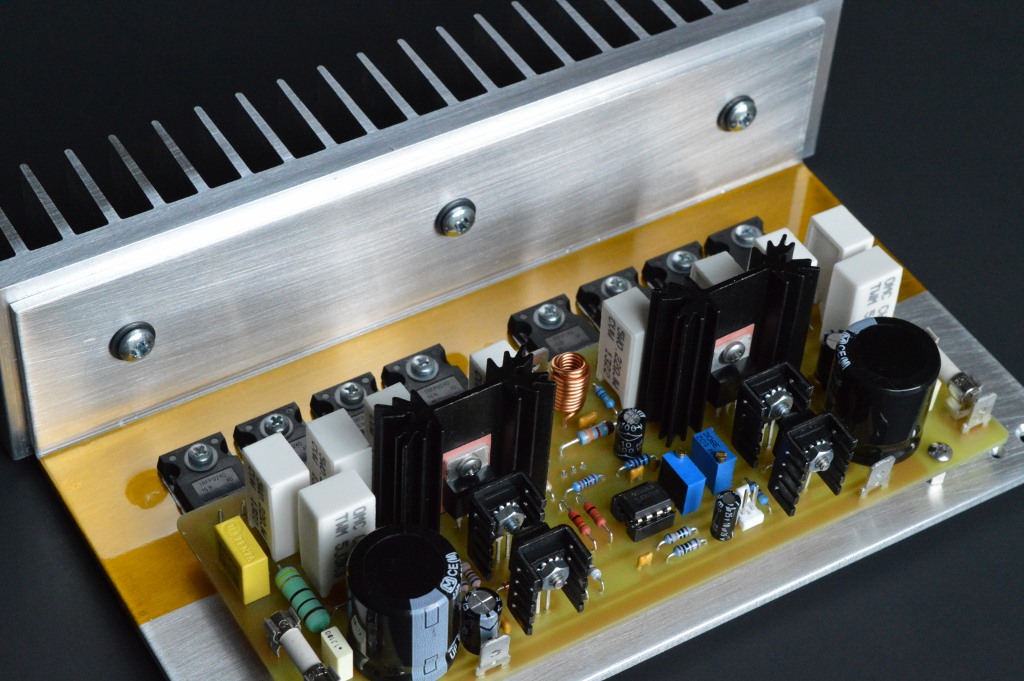
Chip Amplifiers - TDA7293
The TDA7293 is a monolithic integrated circuit in Multiwatt15 package, intended for use as audio class AB amplifier in high fidelity applications. The device is using the BCD technology a mixed bipolar and power MOS devices.
Chip Amplifiers - TDA8950J
This project utilizes TDA8950J a high-efficiency Class D 2-channel audio power amplifier chip. The typical power output is 150Watts per channel with a speaker load impedance of 4Ω. The TDA8950 chip operates over a wide supply voltage range from ±12.5 V to ±40 V and features low quiescent current consumption.
 Project 65 is the fourth in the series of audio power amplifier projects that uses an op-amp in the front-end stage of the amplifier. The CFA-based op-amp input stage is connected to a full complementary hybrid compound feedback pair output stage. Applying a 1KHz 1.84Vpp input signal, the amplifier produces 35.82Vrms across an 8Ω load when connected to a ±56.6VDC power supply rails and a THD of 0.002% as measured by a QA400 audio analyzer. The amplifier sounded powerful enough even though it puts out less than 200watts into an 8Ω load.
 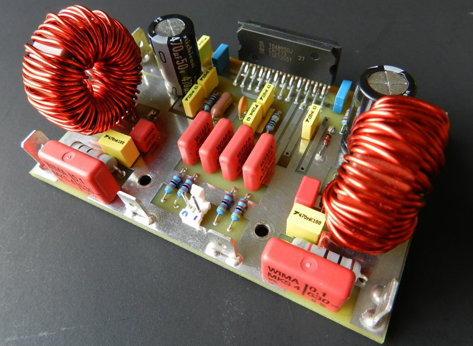 The TDA8950 is a high-efficiency Class D 2-channel audio power amplifier chip. The typical power output is 150Watts per channel with a speaker load impedance of 4Ω. The TDA8950 chip operates over a wide supply voltage range from ±12.5 V to ±40 V and features low quiescent current consumption. For this project the TDA8950 is configured as a mono Full Bridge Class D power amplifier. This configuration was chosen to effectively avoid a strange phenomenon of a typical Class D power amplifier called "pumping effect". The BTL power output is 300watts at 8Ω with ±37VDC PS rails.
  This is another audio power amplifier project in the series that uses an op-amp in the input stage. The prototype is populated with eight 800V/20A/200W NPN power transistors from Fairchild Semiconductor configured in a quasi-complementary output stage topology. These T0-264 packaged power transistors are typically intended in high-voltage color display horizontal deflection circuit applications but performed very well in this project. Initial test results shows that the amplifier is capable of producing a power output of more than 300 watts into an 8Ω load with ±72VDC power supply rails.
  This is another audio power amplifier project in the series that uses an op-amp in the input stage of the amplifier. The complementary 200V 16A 250W TO3-packaged output stage transistors from On Semiconductor are excessively biased about 500mA of current per transistor. The prototype when connected to a ±35VDC power supply rails was able to produce a power output of 50 watts into an 8Ω load with a THD of 0.00186% and a flat 20Hz to 20KHz frequency response as measured by a QA400 audio analyzer. The overly biased amplifier reproduces surprisingly pleasant listening experience.