Project 5
100W MOSFET Audio Power Amplifier
The concept of Project 5 originated from an old Hitachi Semiconductor Power MOSFET Application Notes. The Application Notes explains the characteristics and advantages of using Power MOSFETs in various applications. A typical design of a 100 Watts audio power amplifier was presented as an application for these devices.
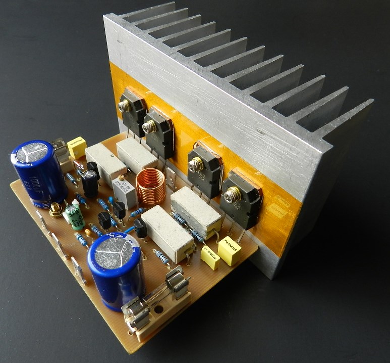
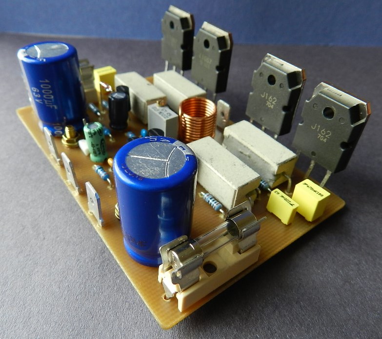
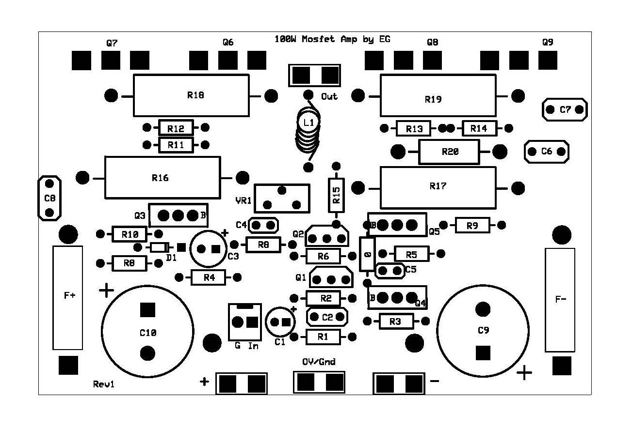
The schematic diagram was redrawn to make it presentable and the Part IDs are the actual components populated on the PCB. If you are planning to build this project, a PCB layout and Project5 100W Mosfet BOM are provided for free, as is, without warranty.
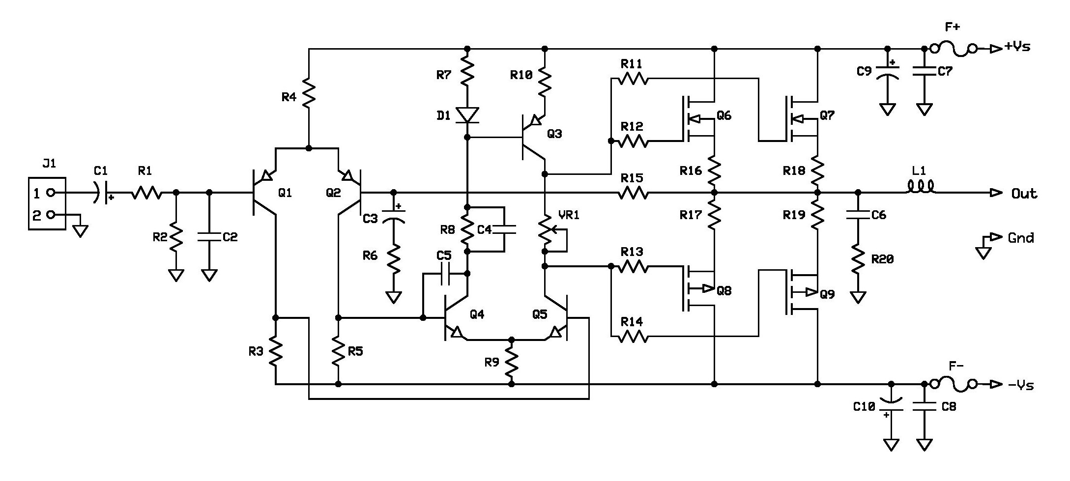
Schematic Diagram of 100W MOSFET Power Amplifier Project
The main power supply rails for this project is ±54VDC. I have tested my model unit at ±30VDC without a hitch. The overall gain of the amplifier is set by the ratio of R15 and R6 in series with C3. The input stage Q1/Q2, is configured as a differential amplifier circuit. The outputs of Q1/Q2 are connected to another differential amplifier Q4/Q5, also described in the notes as a Class A voltage amplifier stage. C4 and C5 were added for high frequency compensation. Q3 and D1 are configured as a constant current source circuit for Q4/Q5. Adjusting VR1 will set the bias current. The output of the voltage amplifier stage drives a push-pull parallel Q6, Q7, Q8 and Q9, configured as a source-follower power output stage. C6, R20 and L1 in the output of the amplifier reduce distortion in the high frequency range, and prevent oscillations when capacitively loaded.
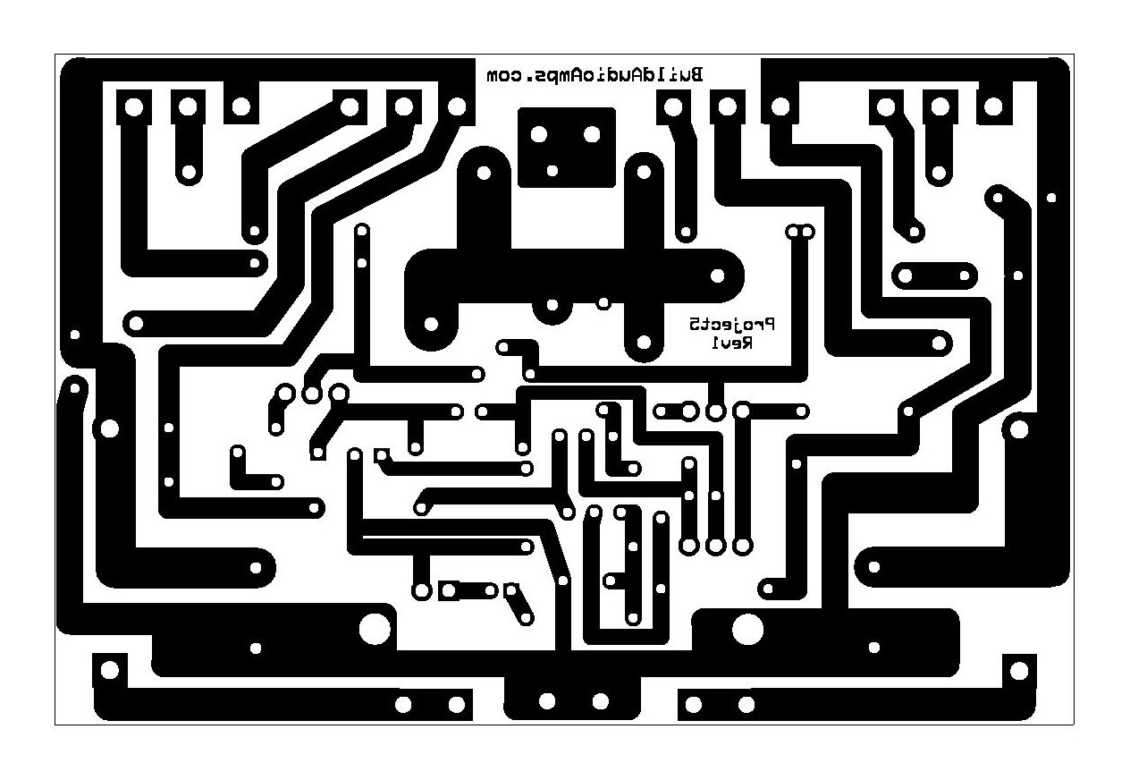
Bottom Copper Layer of PCB
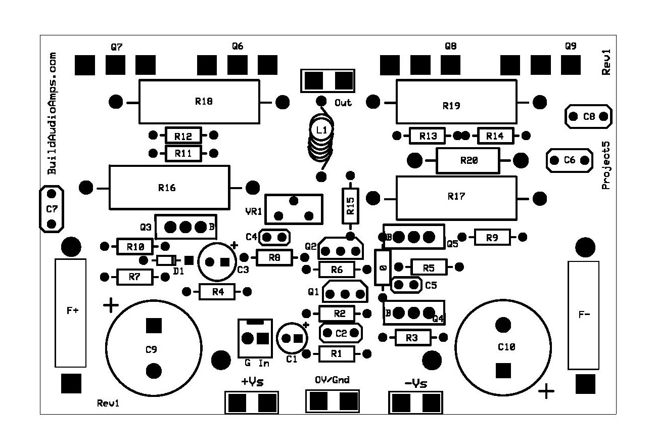
Silkscreen and Parts Placement Layer of PCB
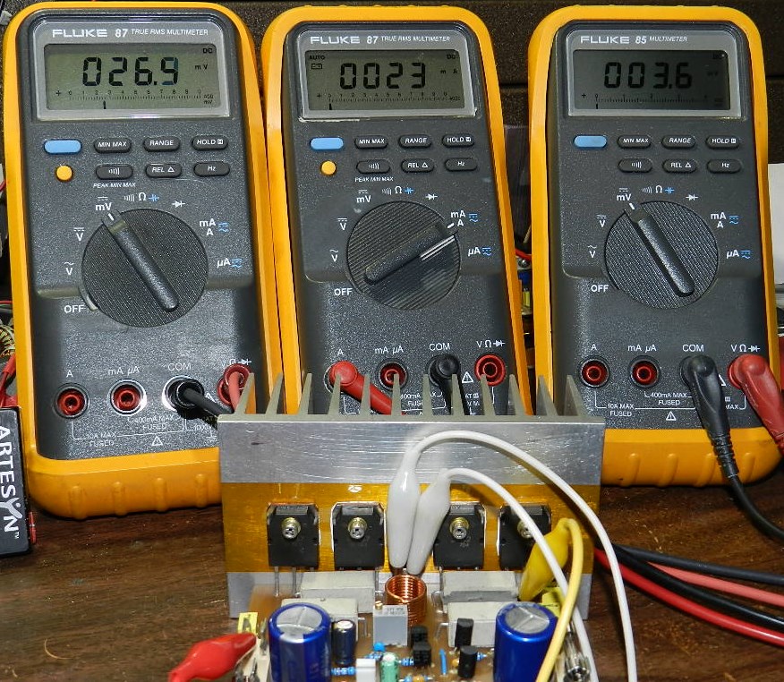
After you have built the Printed Circuit Assembly, you need to adjust the idle current of the amplifier. A shorting jumper or shunt should be installed at the input with no load at the output of the amplifier. A ±30VDC power supply was used for testing.
The DMM on the left of both pictures reads a fixed value of about 26~27mV, the DC offset voltage of the amplifier. The DMM in the middle of both pictures reads about 22~23mA, the overall idle current of the amplifier. The DMM on the right of both pictures measures from 2.2mV~3.6mV, the voltage drop of the source resistors R16 or R18 and R17 or R19. If their readings do not change as you vary VR1, power OFF immediately and check your PCB assembly.
If you plan to use a higher power supply voltage, you may do so at your own risk and DO NOT exceed the working voltage of C9 and C10! The same test procedures should be performed.
Here's a much better way of testing your project:
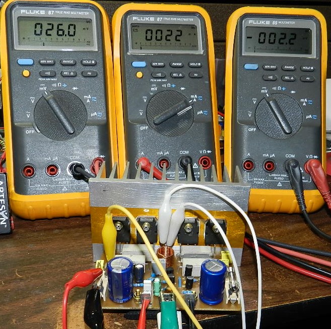
If you have another DMM, you can now monitor the voltages across both N-Channel and P-Channel source resistors. Adjust VR1 and stop adjusting when you reach to a point where both voltage readings will be almost the same but of opposite polarities. As shown in the next picture, 27.1mV is the DC offset voltage, 19mA is the idle current, and 1.8mV across R16 and -1.4mV across R19.

If you obtained the same test results, as shown in the above pictures, switch the power OFF. Connect your favorite music source and test speakers. Adjust volume at the lowest setting and listen. It should reproduce clear, distortion-free music. If you did, crank it up and enjoy!