Project 22
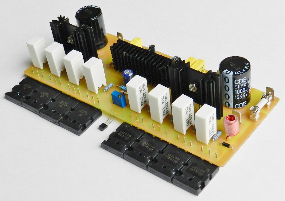
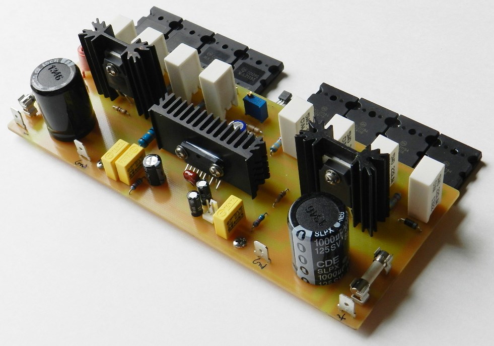
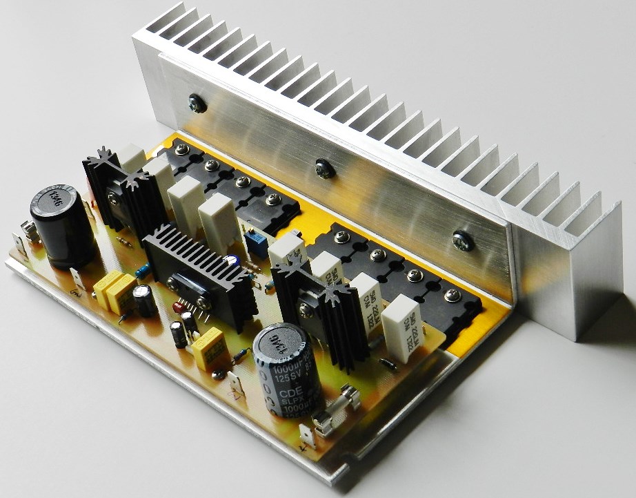
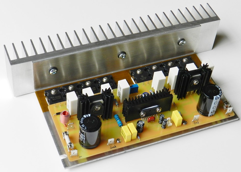
Project 22 is the high power version of Project 8. The schematic diagram is similar to Project 8 except for the addition of a high capacitance speed-up capacitor, C11, at the driver stage. The drivers were replaced with complementary pair TO3-P packaged transistors rated at 17A 250V 130W and configured as emitter-followers. The power output transistors was also replaced with four pairs of TO-264 packaged transistors rated at 16A 250V 200W, also configured as common collector or emitter-followers. To achieve more power output from this project, it is necessary to increase the voltage rails to a hefty ±75VDC or higher, as long as you don’t exceed the maximum supply voltage rating of the LME49811. The power output of this project is 255Wrms at 8Ω or 510Wrms at 4Ω. If a 1KWrms power output at 2Ω load is to be desired, additional power output transistors are required (only for the fearless amp builders!).
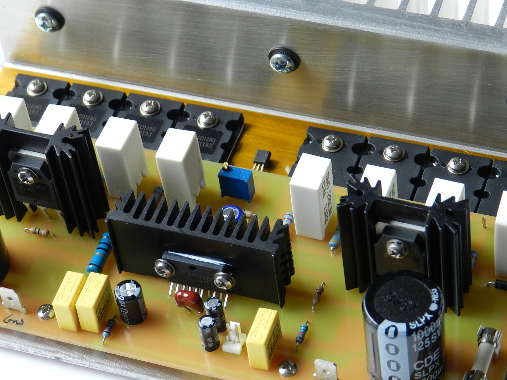
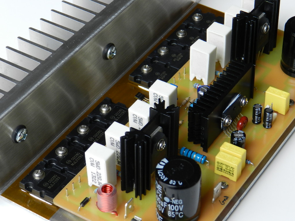
The PCB is populated with SMDs around the LME49811 and Through-Hole components on the power output stage. The model unit shown in the heading pictures above is Rev1 while the silkscreen layer of PCB shown below is Rev2. Changes were made to the PCB layout to remove the resistor on top of R21.The schematic diagrams, BOM and PCB layout for Project 22 are available for free by request, as is, no warranty.
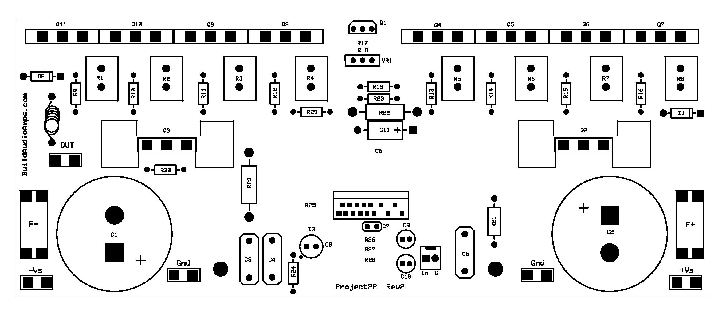 Project 22 Silkscreen parts placement layer of PCB.
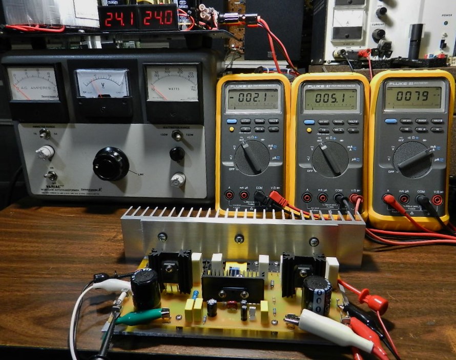

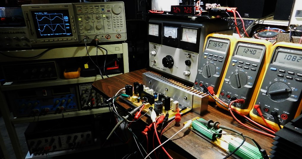
Here’s the fun part! Insert a jumper or shunt at the input of the amplifier. Do not connect any load or loudspeaker at the output of the amplifier. Adjust VR1 to minimum resistance. Prepare 3 DMMs to measure the DC offset voltage, the voltage between the emitters of Q7 and Q11 power output transistors and the current across the F+ fuse terminals. Initially power the amplifier under test with ±24VDC. The picture on the left with a ±24VDC power supply is showing the DC offset voltage at 2.1mV measured at the output of the amplifier, 5.1mV across the emitters of Q7 and Q11 and the current measured across the F+ fuse terminals at 79mA. Gradually adjust VR1 to obtain the 5mV reading after a warm-up period of about 10 minutes. If you get different DMM readings, switch the power supply to OFF immediately and check for PCB assembly errors.
If a Variac transformer is available, connect the AC input of the power supply to the output of the Variac transformer. Switch the power to ON and gradually adjust the Variac’s AC output voltage from zero until the voltage output of the power supply reaches ±75VDC while keeping an eye on unexpected increase in any DMM readings. If you observed an increase in any of the DMM readings switch the power to OFF immediately and check for PCB assembly errors. The picture on the right with a ±75VDC power supply is showing the DC offset voltage at 0.6mV, the voltage across Q7 and Q11 at 5mV and the current across the F+ fuse terminals at 85mA. Readjust VR1 to get the 5mV reading after 10 minutes, after that, you may proceed with music test.
If a Variac transformer is unavailable, make sure that the power supply has been properly assembled and that the output voltage rails have been measured at ±70VDC up to ±77VDC before connecting it to the project. With the power supply at OFF, adjust VR1 for minimum resistance. Switch the power supply to ON; the DMM measuring the voltage across Q7 and Q11 should read less than 1mV. The current across the F+ fuse terminals should be less than 85mA. If the DMM reading is more than 1mV and cannot be adjusted, power OFF immediately and check for PCB assembly errors. If the DMM reading is less than 1mV, wait for 10 minutes for the amplifier to stabilize and then gradually adjust the reading to 5mV.

The next test procedure is optional, but if an oscilloscope, audio signal generator and 8Ω dummy load are available, the maximum power output of Project 22 before clipping occurs can be measured. Do not touch the heat sink or the dummy load during this test; they will get extremely hot!
The power output was measured using an HP3312A Function Generator set at 1KHz 3.52Vp-p sine wave output and connected directly to the input of the amplifier under test as well as the CH1 test probe of the oscilloscope. An 8Ω/400Watt dummy load was connected at the output of the amplifier under test as well as the CH2 test probe of the Tektronix TDS520D 500MHz Digital Phosphor Oscilloscope. The amplifier produces 45.2Vrms across the 8Ω/400W dummy load or a power output of about 255Wrms, as shown in the TEK hardcopy picture on the right. The oscilloscope’s horizontal scale was adjusted at 200uS to verify for any visible clipping on its peaks. Project 22 was paired with the LM1036 tone control project and the sound quality it reproduced did not disappoint!