Project 58

Project 58 is the quasi-complementary version of Project 44. The project features a cascoded complementary differential input stage as well as the voltage amplifier stage. Instead of the three-stage complementary common collector amplifier output stage, Project 58 utilizes the BJT quasi-complementary output stage topology with a Baxandall-diode at the PNP driver transistor. The performance is nearly the same as any emitter-follower output stage topology. However, quasi-complementary designs have cost-effective advantage over full complementary since PNP power transistors are always more expensive than the NPN types. It is also a suitable buildamp choice for high-power audio power amplification as in outdoor sound reinforcement applications.
For a brief description about the input stage used in Project 58, please refer to Project 44’s project page. Project 58’s schematic diagram will be referred to from hereon. The project may be connected to a ±55VDC to ±75VDC power supply rails. At ±65VDC rails, the prototype produces 42.8Vrms before clipping occurs across an 8Ω load with a 1KHz sine wave input signal of 2.88Vms. This corresponds to a power output at 229watts into 8Ω or higher with lower impedance loads and depending on an adequate power supply. Surprisingly, the prototype does work, but not recommended, with ±5VDC power supply rails and still produces decent audio quality. The prototype was also tested into a 2Ω load with no problems.
Although the front-end circuit works well in Project 44; however during initial test of Project 58, distortion occurs on the lower half of the output signal waveform as shown in Figure 1. This was hardly noticeable during listening test. To fix the problem, the locations of C4 and C5 have been modified in both the positive and negative voltage amplifier stages. Once C4 and C5 were inserted into the circuit, this totally eliminated the distortion as shown in Figure 2.

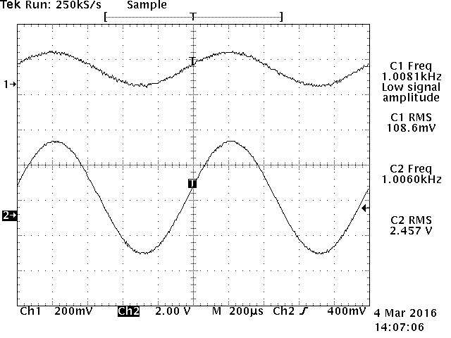
Figure 1. Initial test result of Project 58. Figure 2. Test result of Project 58 with C12 in the circuit.
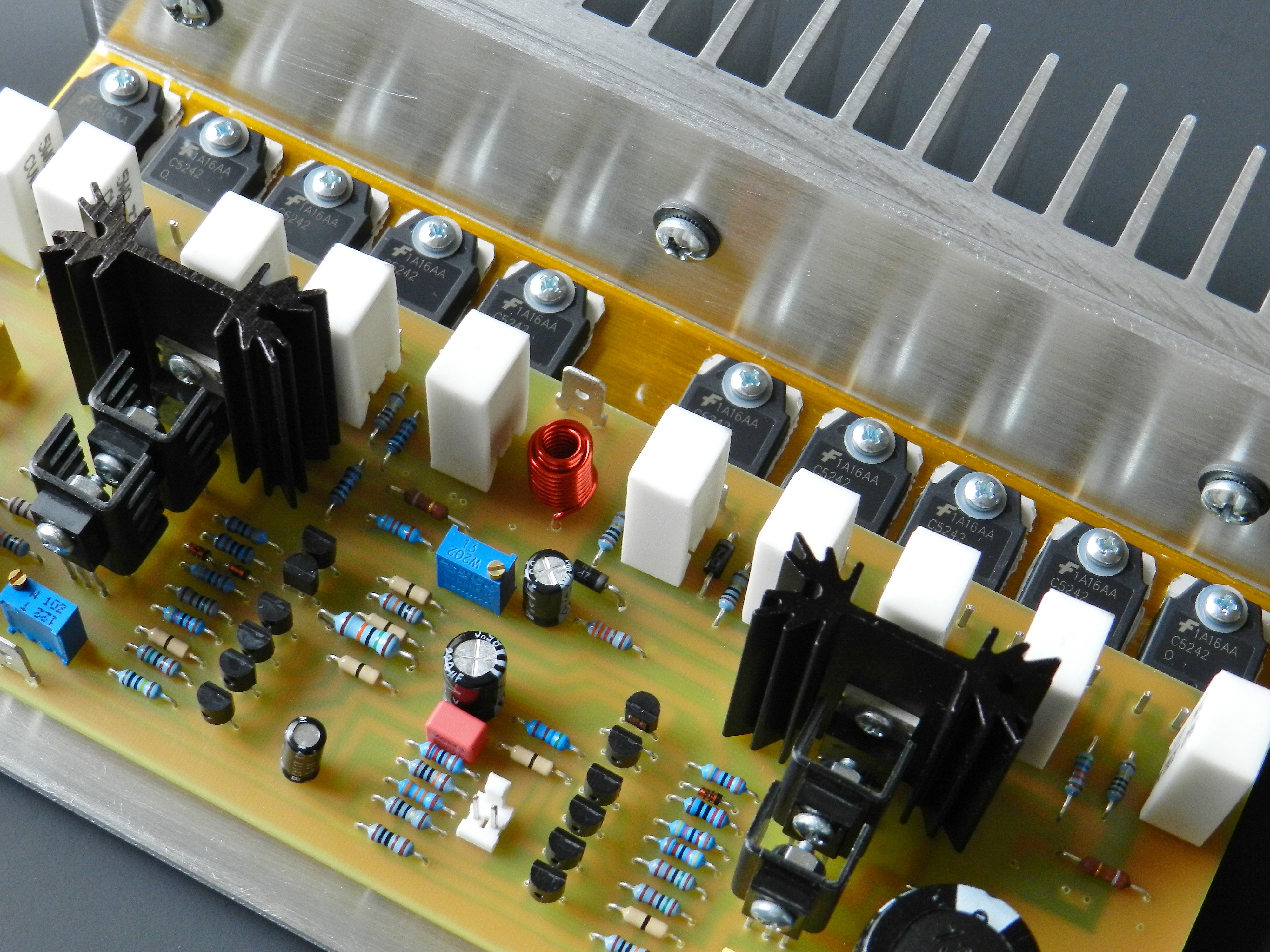
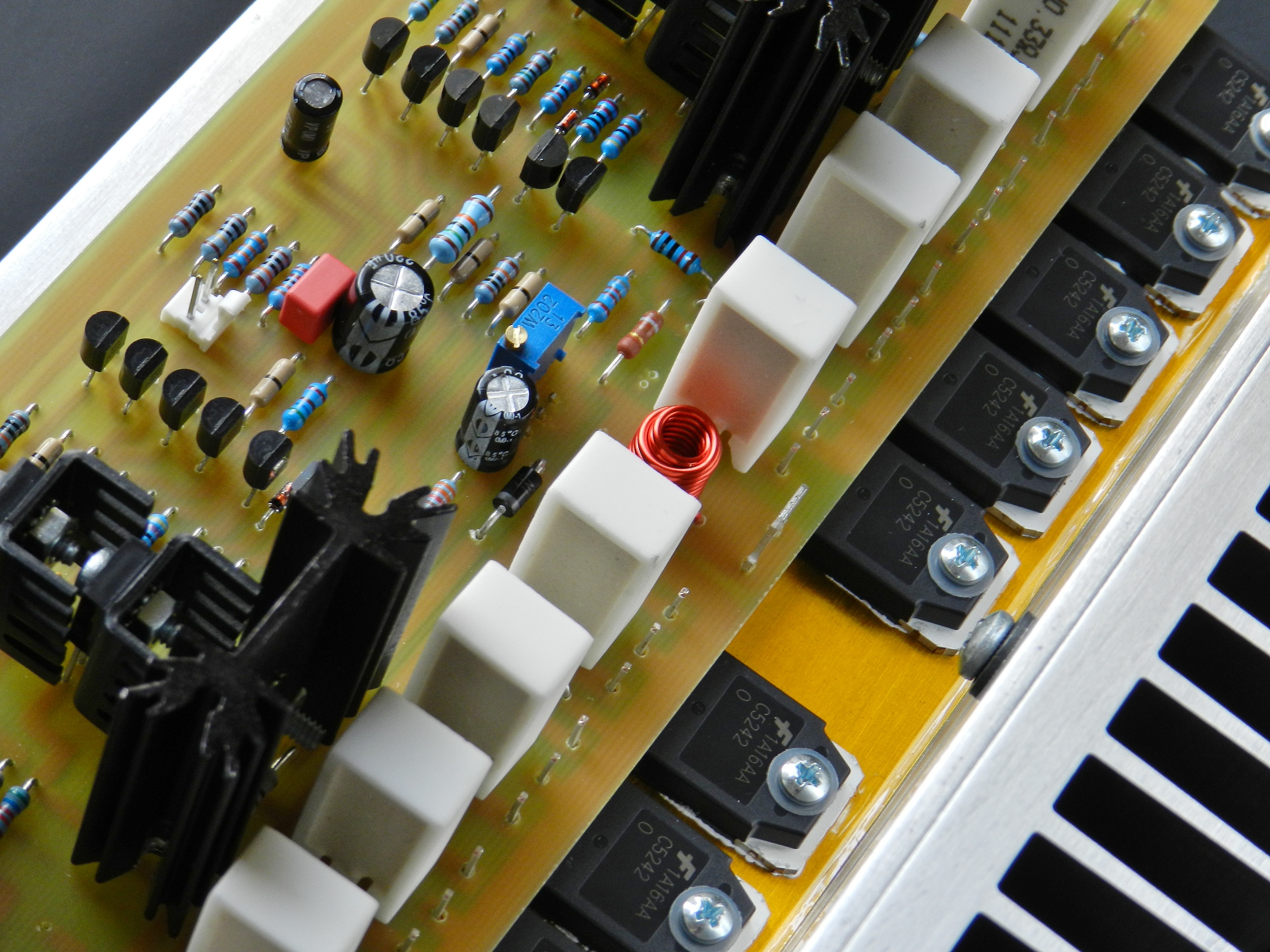
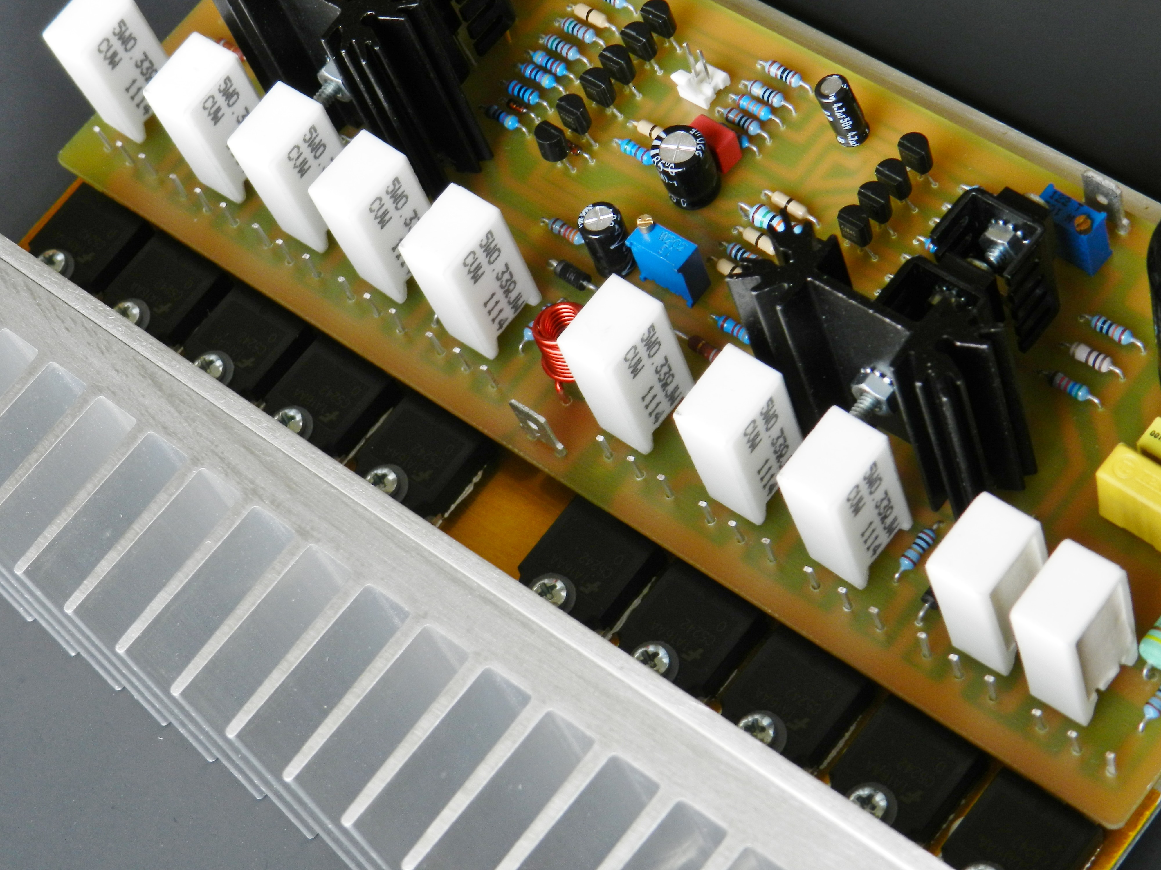
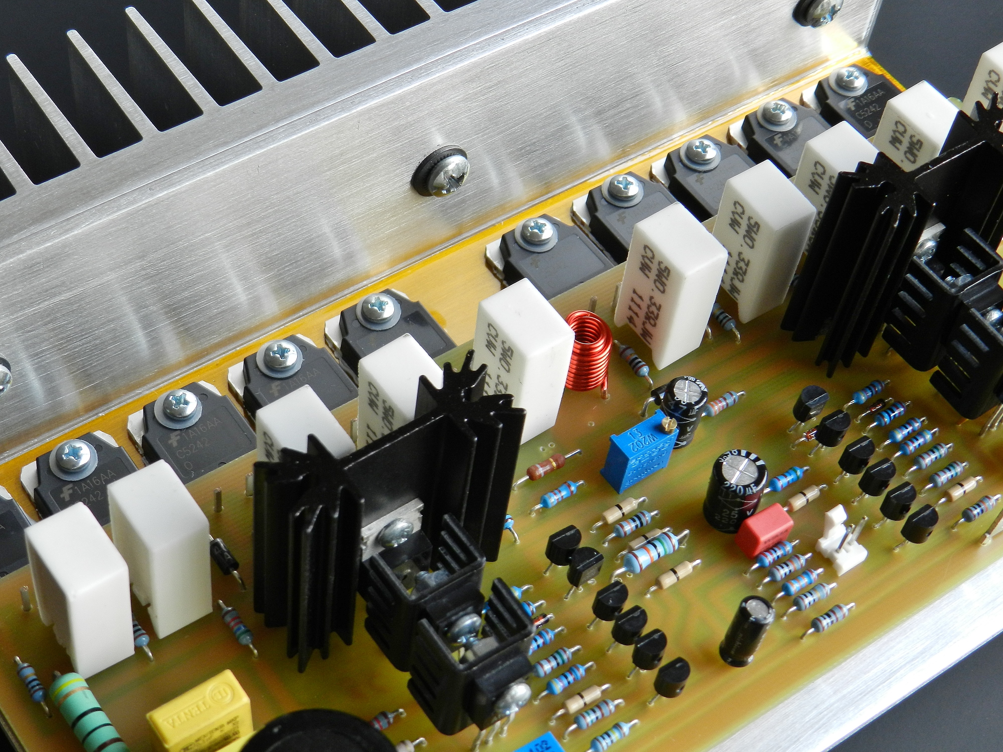
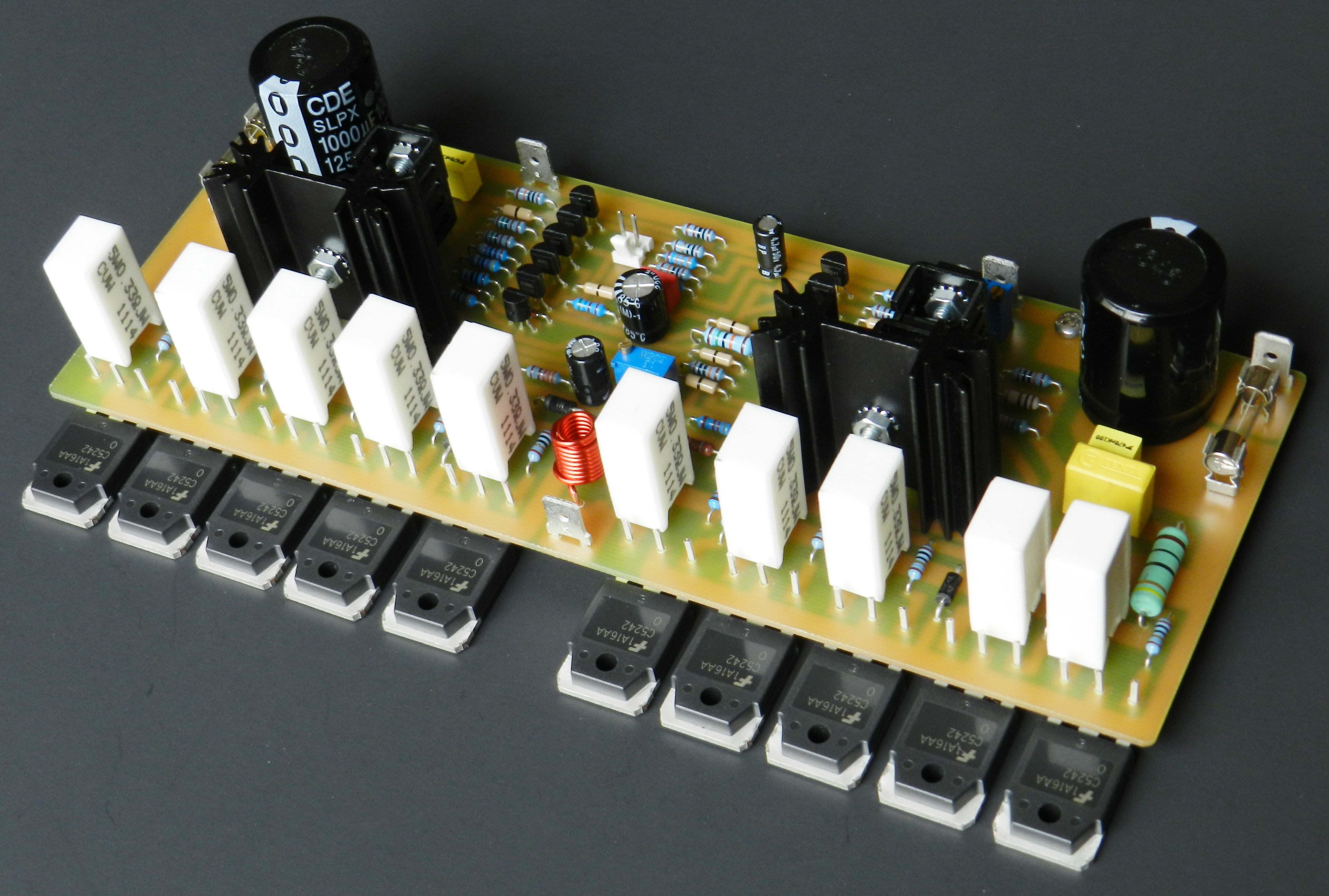
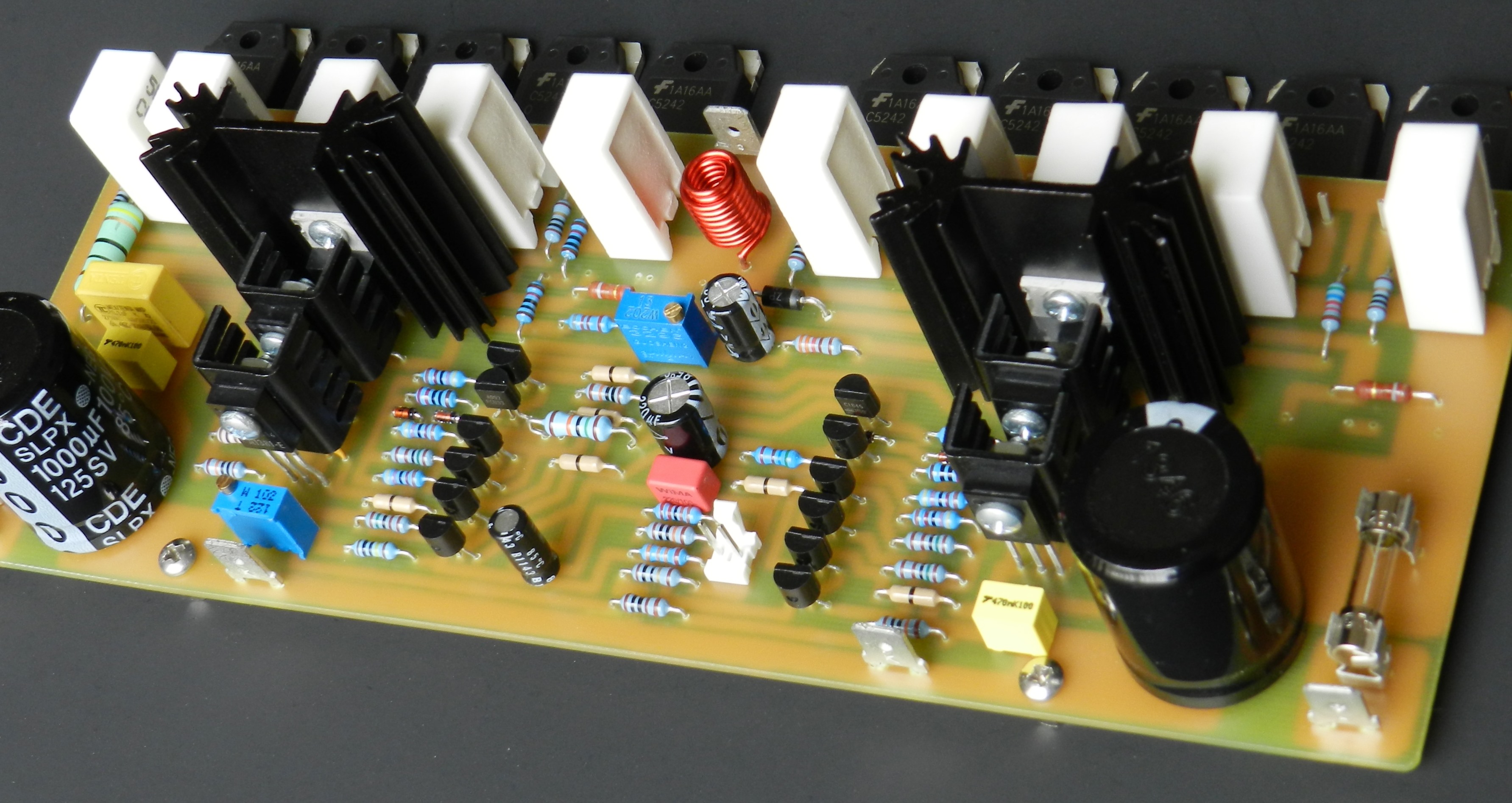
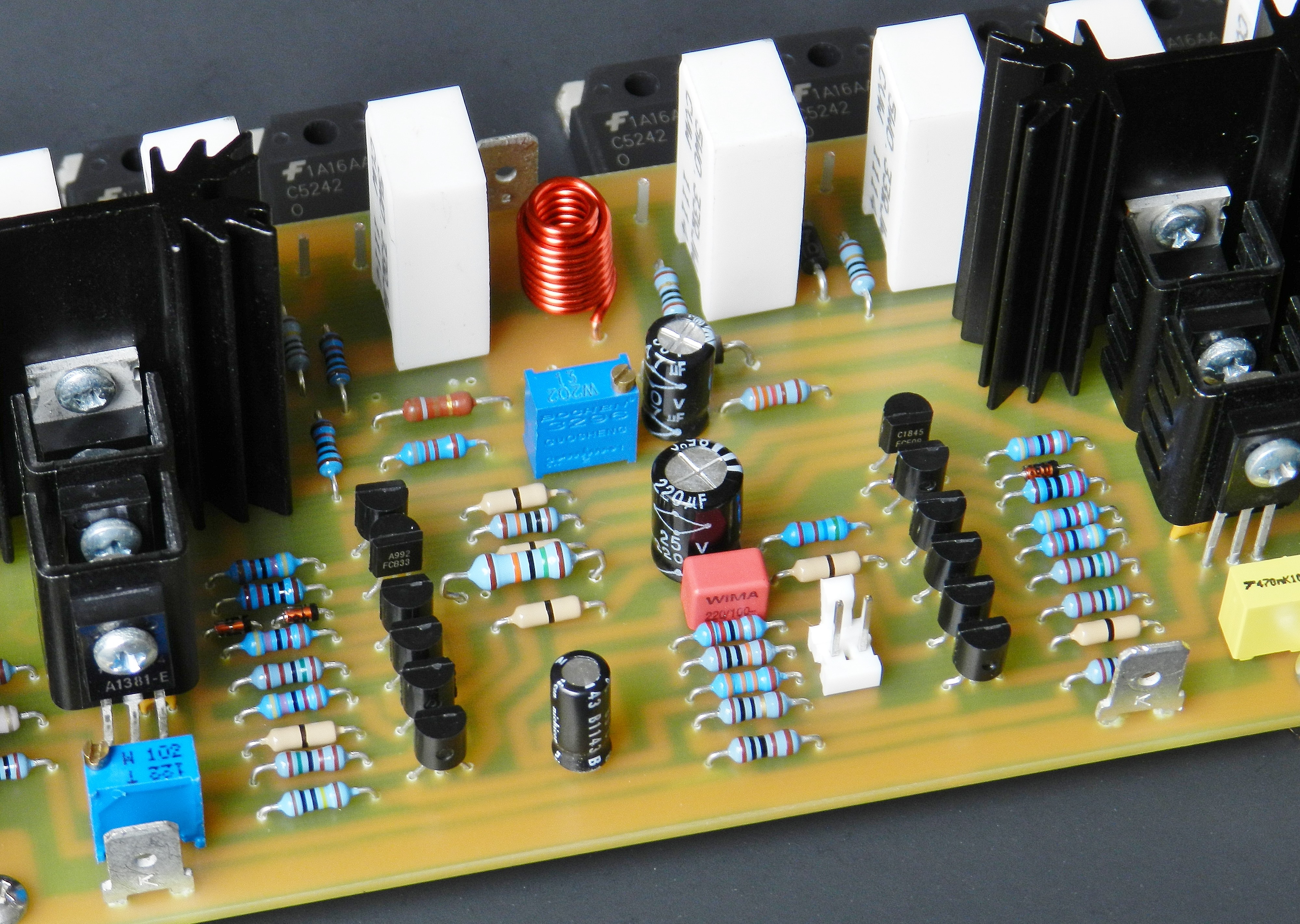
The PCB layout was created using the ExpressPCB software, laser-printed and etched to an 8” X 3” single-side PCB. All the components used in the prototype model are standard available parts. If you are interested in building this project and have read the Information and Policies section of the website, the schematic diagram, PCB layout and BOM (available only by request) are free, as they are, no warranty.
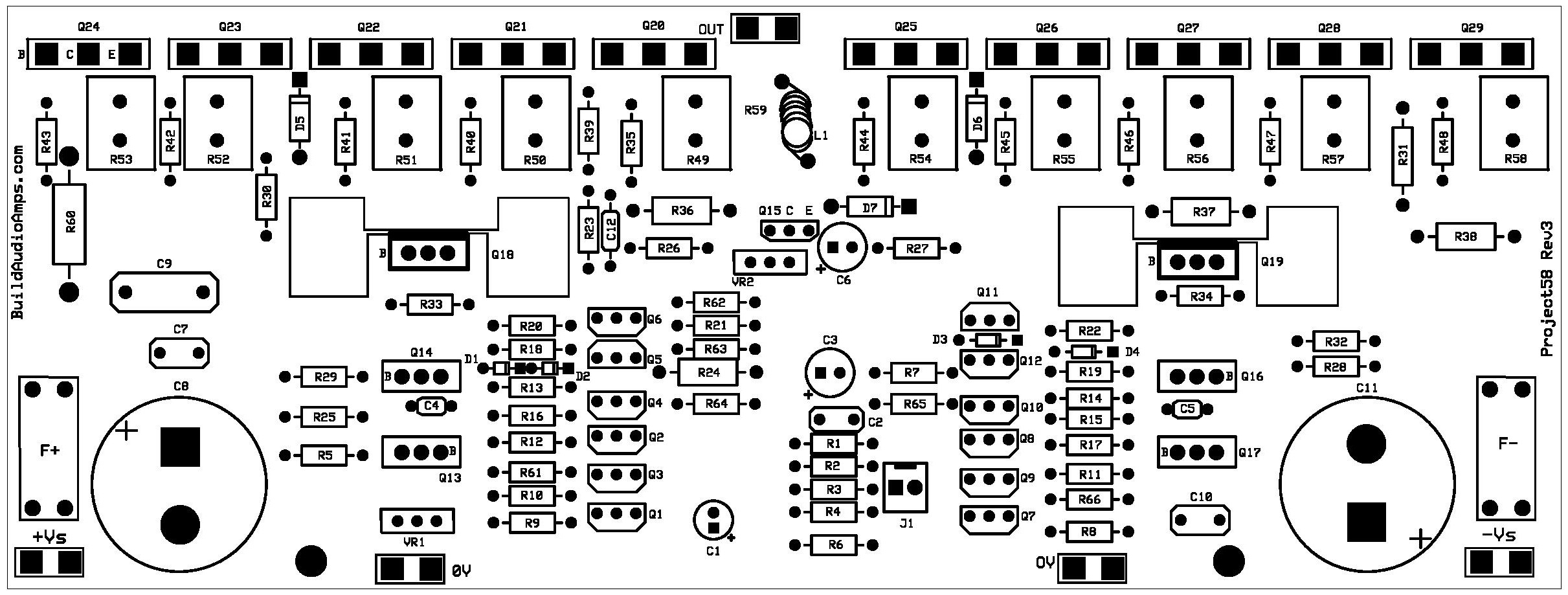
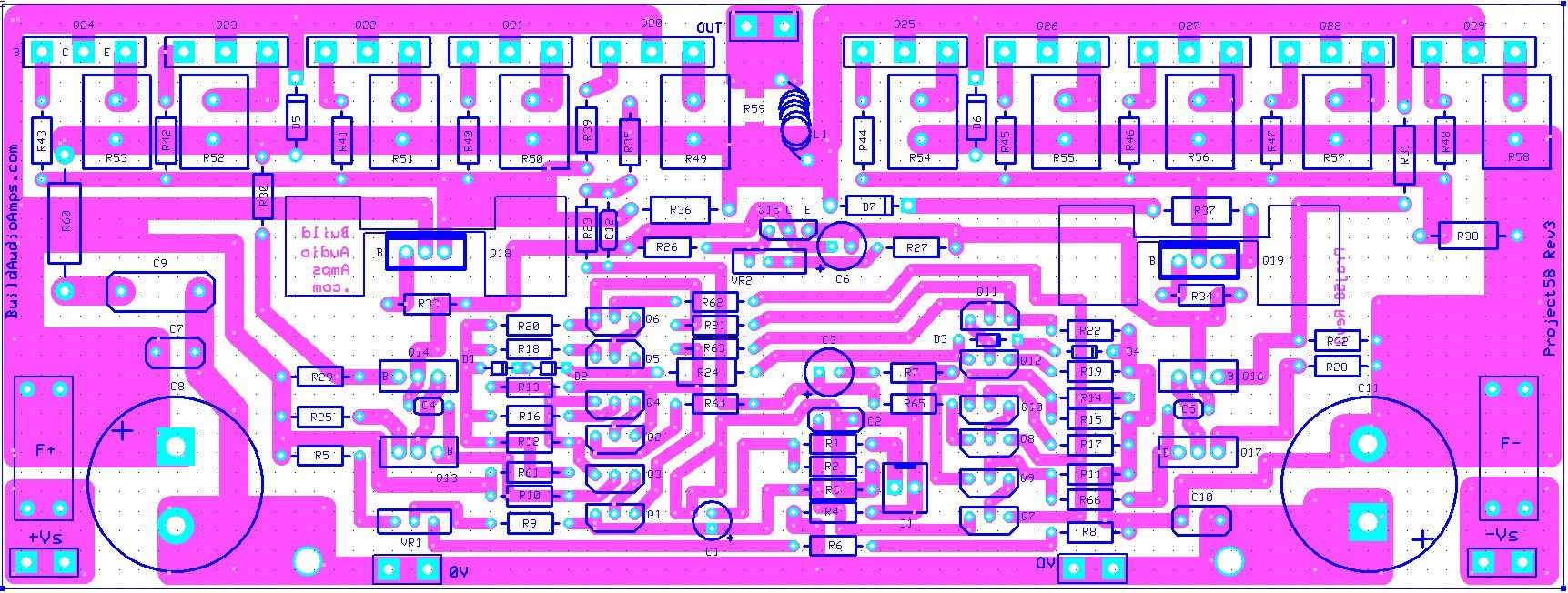
Figure 3a. Project 58 Silkscreen top layer of PCB. Figure 3b. Project 58 Top and Bottom layer of PCB.
If you have decided to build this project and assuming an error-free assembly, make sure to adjust VR2 to maximum resistance before applying power to the project. Figure 5 shows the initial test setup of the prototype, which is connected to a ±64VDC power supply rails, an 8Ω dummy load and no input signal. The DMM on the left is connected to the output of the amplifier. The DMM measures the DC offset of the amplifier at 1.4mV and this may be adjusted by VR1 as close as possible to 0mV. The DMM in the middle is connected across R53, the emitter resistor of Q24. With no input signal there is no voltage drop across this resistor, hence the 0mV reading of the DMM. The DMM on the right is connected across the F+ fuse terminals; this measures the overall current drawn by the amplifier at 14mA.

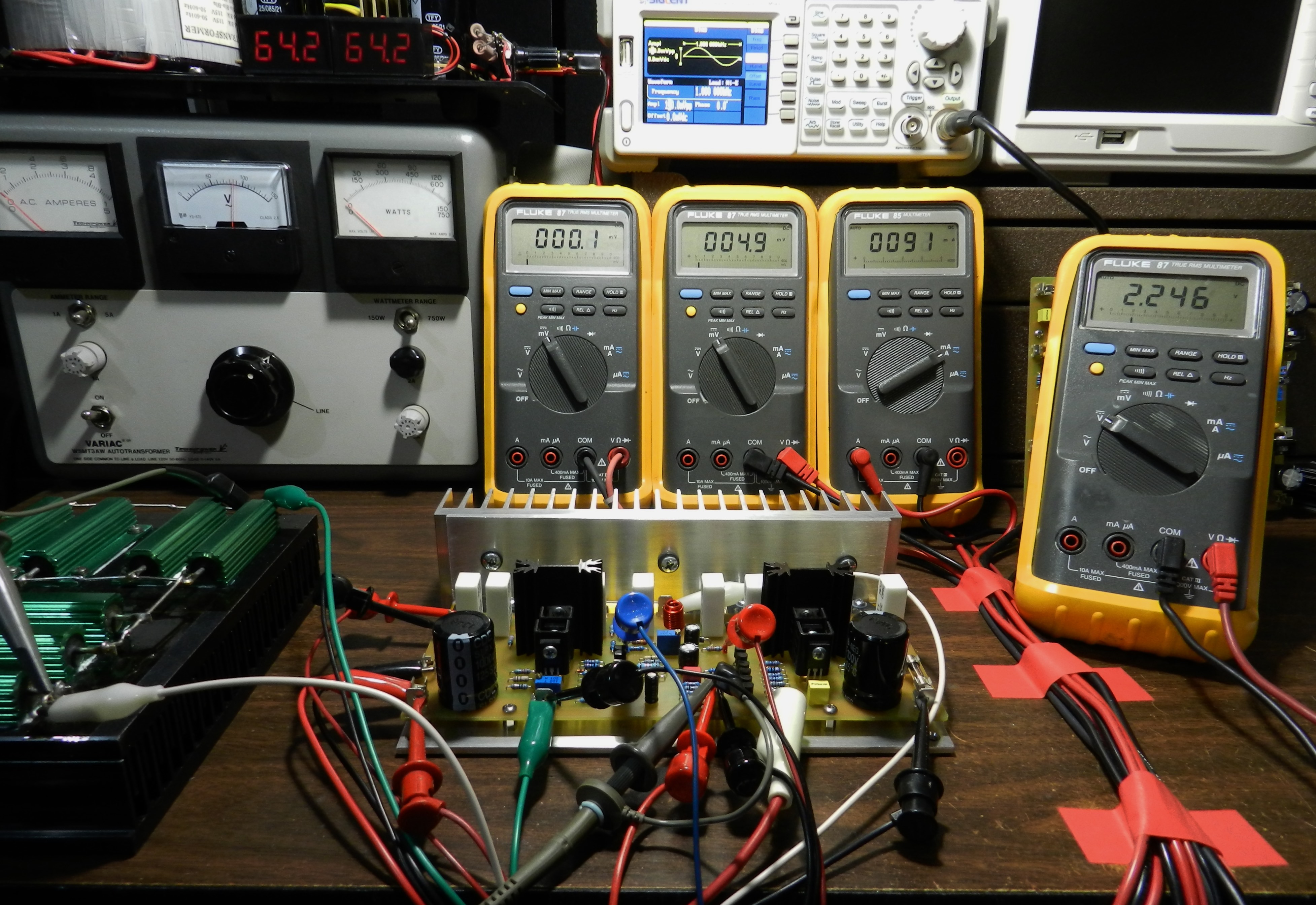
Figure 5. Initial test setup of Project 58’s prototype. Figure 6. Another DMM measures the voltage across the bases of Q18/Q19.
Shown in Figure 6 is another DMM that was added in the test setup. This DMM is connected across the bases of driver transistors, Q18 and Q19, through R33 and R34. The blue and red test clips, seen in the middle on top of PCB module, are connected to one side of each resistor, R26 and R27. This DMM will measure the amount of bias needed by the power output transistors to eliminate crossover distortion as shown in Figure 7 (see red arrows). A 1KHz at 100mV sine wave input signal was applied to the input of the amplifier. An oscilloscope is connected at the output of the amplifier across the 8Ω dummy load. To adjust the bias, observe the waveform in the oscilloscope while slowly adjusting VR2 and stop until the crossover distortion is eliminated. The correct bias was measured at 2.246 volts (to about 2.5 volts). This bias will reduce the crossover distortion as shown in Figure 8. With the properly determined bias, the voltage drop across R53, the emitter resistor of Q24, measures at 4.9mV (to about 6mV), while the overall current drawn by the amplifier is 91mA (to about 100mA) as shown in Figure 6. Turn the power supply to off and allow the amplifier to cool down. When you apply power to the cold amplifier, the voltage drop across R53 is about 27mV and the overall current drawn by the amplifier is about 450mA; don’t panic, this will eventually go down after a few seconds.
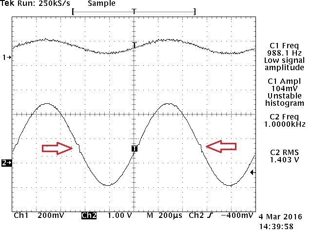
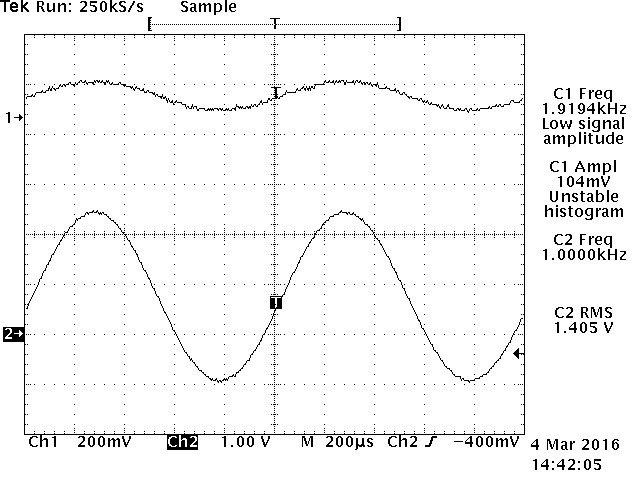
Figure 7. Output waveform with crossover distortion. Figure 8. Output waveform when bias is properly adjusted.
If you are planning to do the next optional test and higher power supply rails are used, extreme caution and alertness must be observed. Be careful not to touch the heatsink, it will get very hot during this test. The optional power output measurement setup is shown in Figure 9, while the captured waveforms test result is shown in Figure 10. The amplitude of the 1KHz sine wave input signal was adjusted before clipping at 2.88Vp-p and this produces 42.8Vrms across the 8Ω dummy load. This test will push the amplifier’s components to its limit. This continuous stressed operating condition must be avoided for long periods of time. If you intend to run this test longer, then to avoid permanent damage to the components adequate forced air-cooling is necessary. Also watch the DMM readings they will be your best friend at this time.
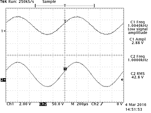
Figure 9. Test setup for power output measurement. Figure 10. Power output waveform before clipping.
A QuantAsylum’s QA400 24-bit 192Ksps USB Audio Analyzer and a QA190 low-noise differential probe were utilized to measure noise, total harmonic distortion, SNR and frequency response of the prototype. Figure 11 shows the basic test setup while Figure 12 shows the test result.
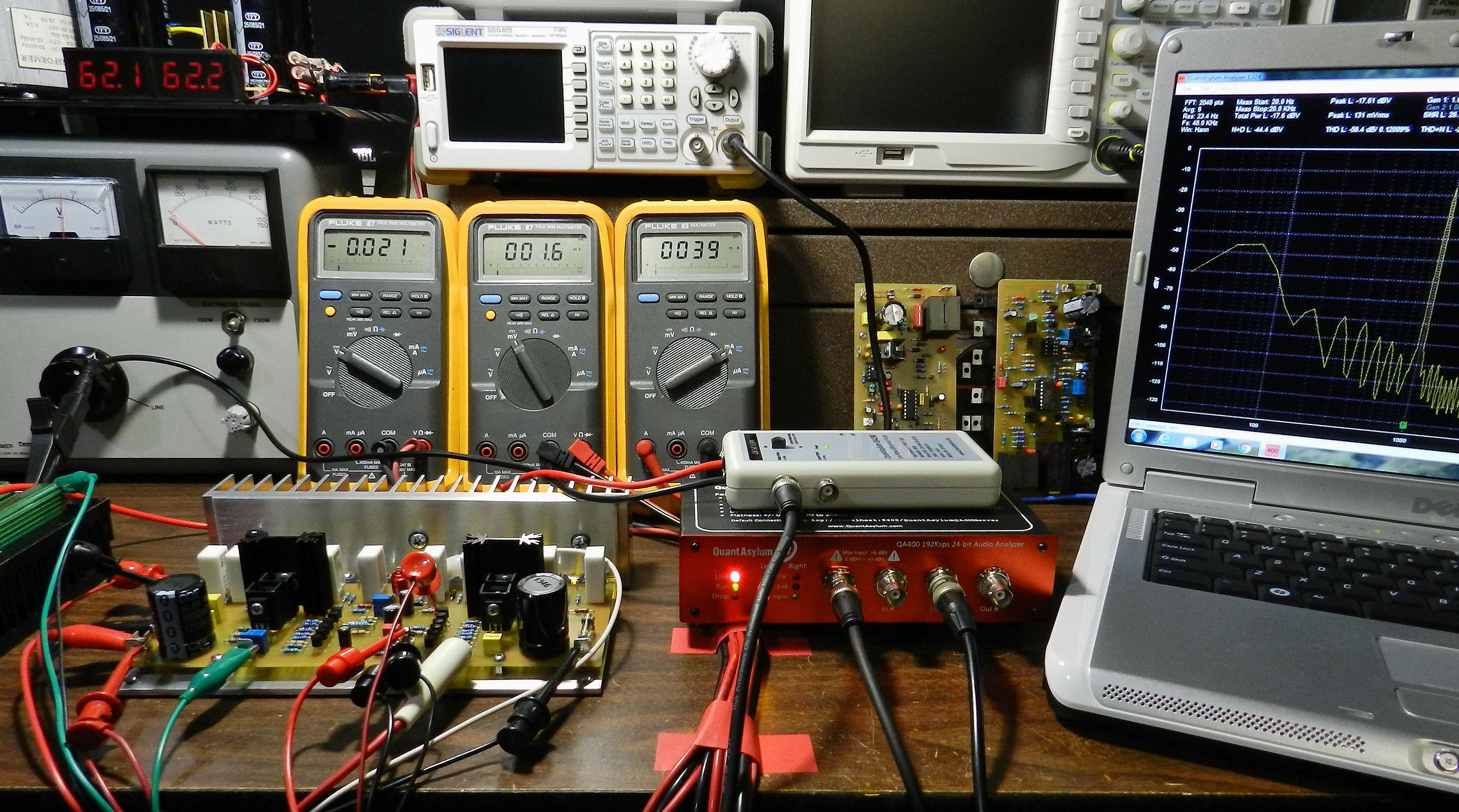
Figure 11. QA190 and QA400 Audio Analyzer test setup.
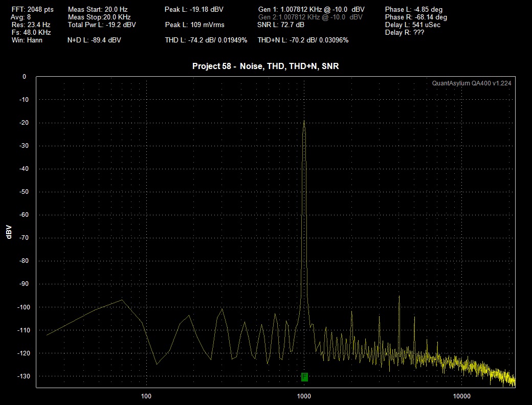
Figure 12. Captured QA400 test result for Noise, THD, THD+N and SNR.
How does it sound? The prototype unit was connected to a modified LM49720 tone control preamp. While playing “Desire” and “Thanks To You” by Boz Scaggs from his “Dig” album on a Toshiba HD-A2 player and several test speakers, you hear pleasing sonic quality. With the same setup and this time for endurance music testing, the entirety of Gabrielle Roth’s “The RMX” album was auditioned louder than normal listening level; this is where it gets its superiority. Several CDs of different genres were also played for the listening test session.