
Project 10
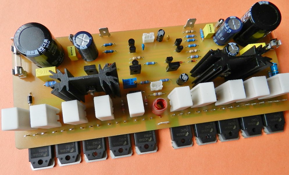
Project 10 is rated at a continuous power output of 130 watts into 8 ohms. The schematic diagram looks complicated but it is fairly straightforward. The input stage is a full complementary differential circuit consisting of Q1/Q2 and Q3/Q4, current-sourced by Q5/D1/D2 and Q6/D3/D4 respectively. The output of the input stage is connected to a full complementary voltage amplifier Q7/Q8. Bias for the output power transistors is thermally controlled by Vbe multiplier, Q9 and initially adjusted by VR1. Pre-drivers Q10/Q11 and Q12/Q13 are configured similar to a T-circuit topology that was very popular decades ago. The emitter follower power output stage uses 5 pairs of my favorite complementary pair 2SC5242/2SA1962 power transistors, more than enough to attain 130 watts at 8 ohms without circuit protection (with the exception of D5 and D6) at ±54VDC supply rails.
The idle current of the amplifier is adjusted by VR1 after a warm up period. With the power OFF, install a jumper or shunt at the input of the amplifier. Remove F+ fuse and insert a DC milliammeter at its terminals. Do not connect any load or speaker, instead connect a DC millivoltmeter at the emitter of Q18 and junction of R28/R39. With the power ON, adjust VR1 to read from 1mV to about 2mV. At 1mV the current at F+ fuse terminals is about 58mA and at 2mV is about 71mA. The DC offset voltage at the output of the amplifier is about 18 to 20mV. The DC power supply to test this Project was adjusted at ±30VDC.
For music test, I use Project 9 as the preamp and the music quality was excellent, if not one of the best sounding audio amplifiers built in my workshop! If you want to build the project a PCB layout, schematic diagram as well as Project10 BOM are provided free by request, as is, without warranty.
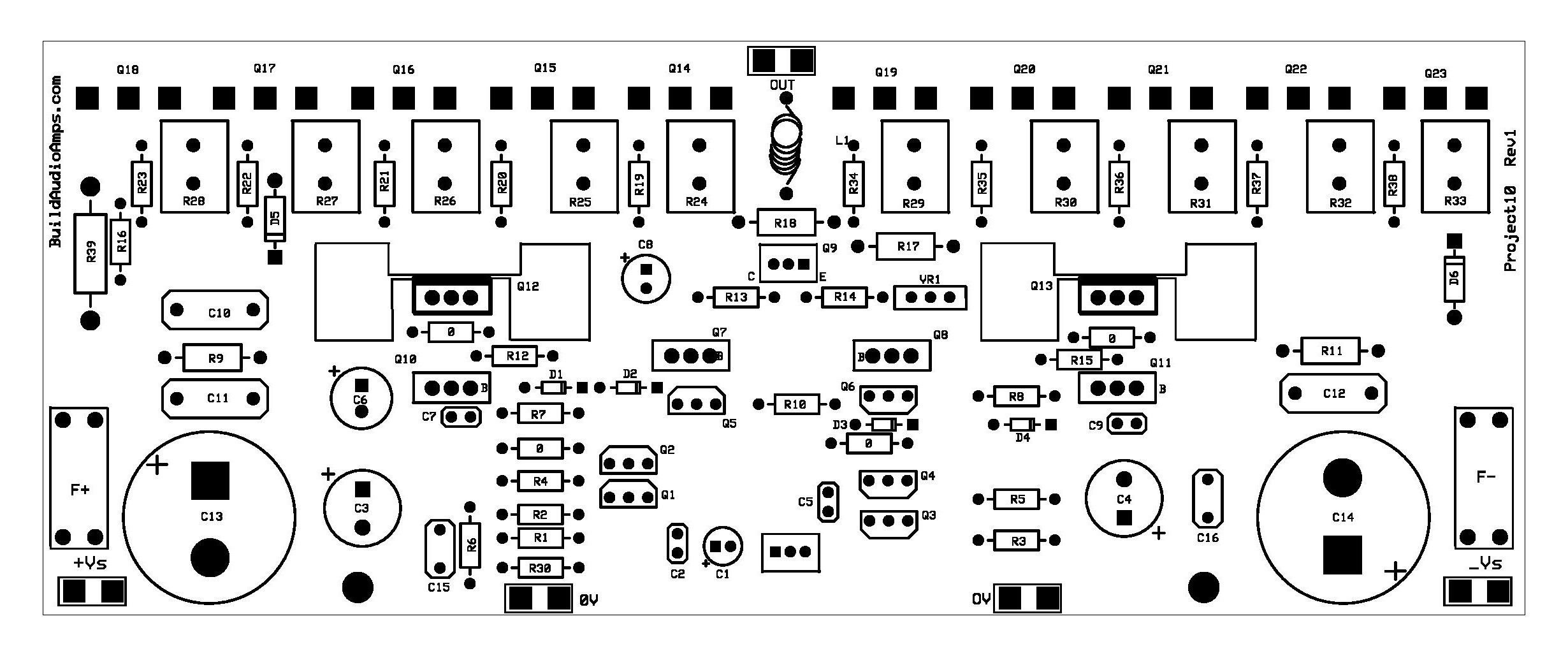
Project 10 Silkscreen Parts Placement Layer
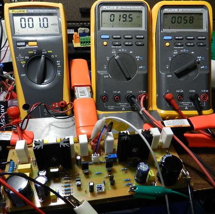
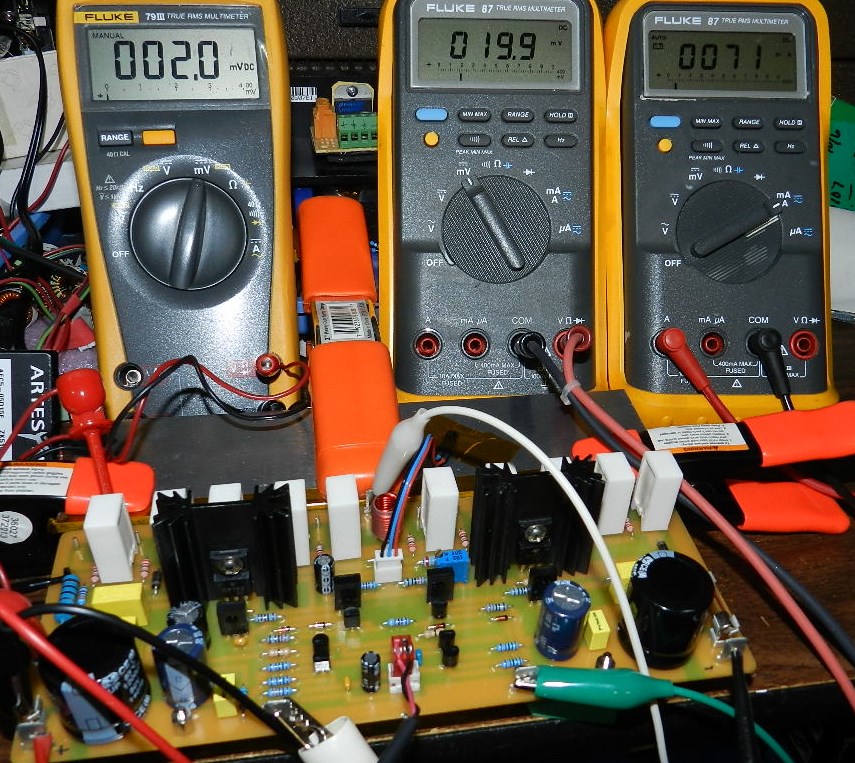
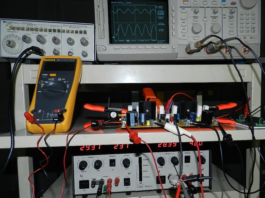
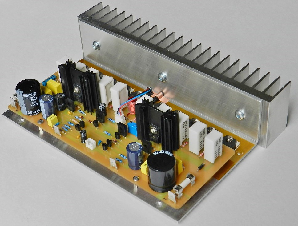
Project 10 under test. VR1 was adjusted to read a voltage drop at the emitter resistor of Q18 about 1mV to 2mV as shown by the DMM on the left of both pictures. The DC offset voltage is about 19mV as shown by the DMM in the middle. The current readings at V+ fuse terminals are 58mA for 1mV and 71mA for 2mV drop across R28. You may wonder, what those clamps doing in there! It's a quick and easy way of adding a heatsink to the power transistors of an amplifier under test. They are made up of 2 pieces of 2" x 8" x 1/4" aluminum plates insulated with polyimide film tapes on one side.
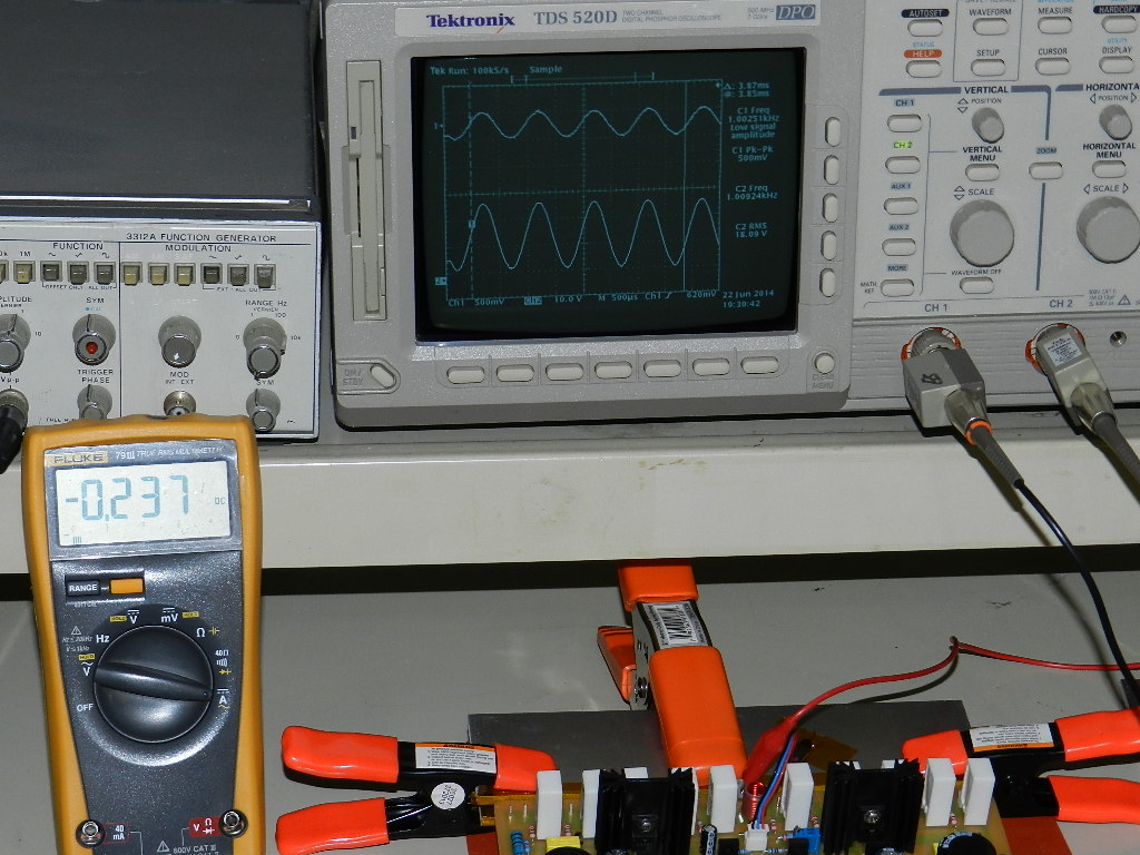
More tests for Project 10. With a ±30VDC test power supply rails, 1KHz 500mVpp sine wave input signal, 8Ω 100Watts load, the power output just before clipping is about 40Wrms. The DMM is reading the current of 237mA at the V+ fuse terminals.
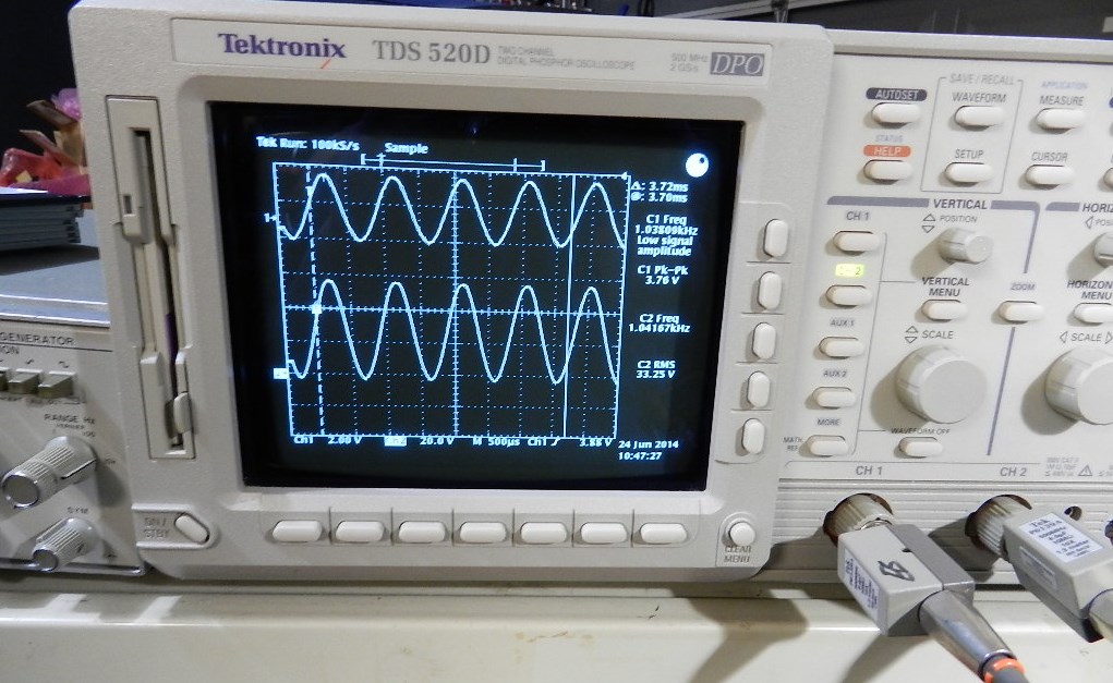
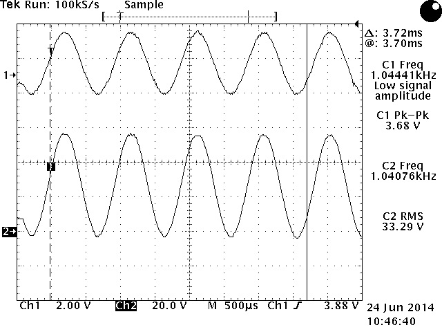
More tests using ±54VDC power supply. With the function generator set at 1KHz 1.3Vrms (3.68Vpp) sine wave output, Project 10 produces a 33.29Vrms across the 8Ω 400Watts load resistors (8Ω 100W X 4 green heatsinked resistors shown in picture) or a power output of about 138Wrms just before clipping occurs. Again excuse my workbench clutter.
![]()