
Project 38
The concept for this project was presented earlier with an Emitter-Follower power output stage. Project 38 will follow-up with a different power output stage, a Complementary Feedback Pair also popularly known as the Sziklai pair, to improve linearity as proven in previous projects. This project will use the same intriguing complementary symmetrical front-end circuitry, which in my opinion works well when combined with other power output stage topologies. The measured power output of this project is about 120 watts at 8Ω or 240 watts at 4Ω with a ±49VDC to ±55VDC power supply rails.
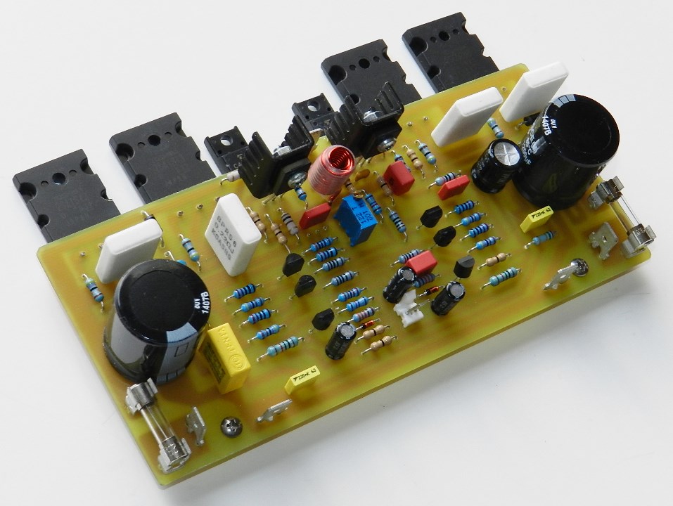
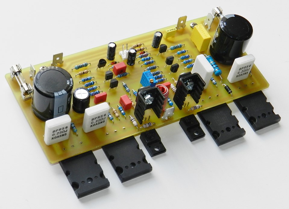
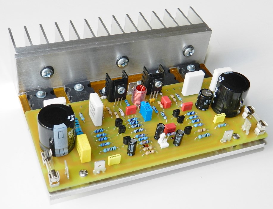
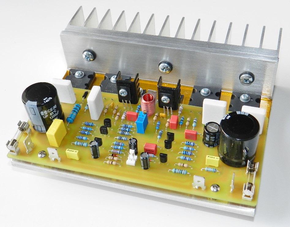
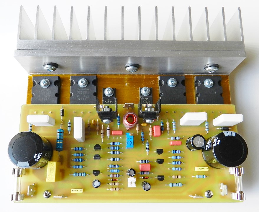
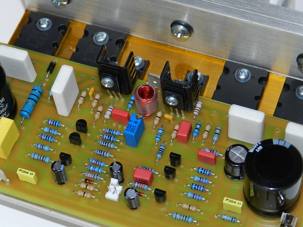
Please refer to the schematic diagram from here on. The input stage of the project consists of two differential amplifiers, Q1, Q2 and Q5, Q6 loaded by two current sources, Q3, D1 and Q4, D2. The current sources are adjusted to about 2mA and determined by the value of R8 and R9. The output of Q1 and Q5 are connected to the common-emitter configured voltage amplifier transistors, Q7 and Q8, high frequency compensated by C8 and C10. The outputs of the voltage amplifier stages are connected to the CFP configured power output stage transistors, Q10, Q12 and Q13 for the positive side and Q11, Q14 and Q15 for the negative side. The bias of the power output transistors is set by VR1 and Q9. The next picture below is showing Q9 populated at the bottom copper layer of PCB and applied with a generous amount of Wakefield’s Thermal Compound P/N 120-8 or similar, to fill-up the gap between the TO-92 packaged transistor and aluminum bracket. The gain of the amplifier is set by the value of R23 and R20 at about 23dB. An interesting feature of this project is the addition of C11 in parallel with R20 and C15 in parallel with R23. Both capacitors audibly improve the overall frequency response of the amplifier, as mentioned earlier in Project 34.
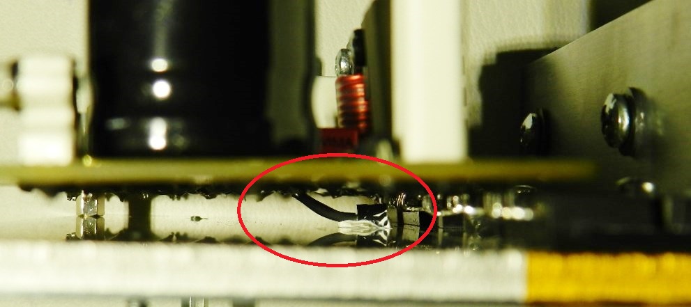 Encircled is Q9 populated at the bottom copper layer of PCB.
John L. Linsley Hood published an article entitled “Simple Class A Amplifier” that appeared on the issue of Wireless World in April of 1969, and here’s a portion of the transcript of what he had to say about listening test:
“It would be convenient if the performance of an audio amplifier could be completely specified by frequency response and harmonic distortion characteristics. Unfortunately, it is not possible to simulate under laboratory conditions the complex loads or intricate waveform structures presented to the amplifier when a loudspeaker system is employed to reproduce the everyday sounds of speech and music; so that although the square wave and low-distortion sine wave oscillators, the oscilloscope, and the harmonic distortion analyser are valuable tools in the design of audio circuits, the ultimate test of the final design must be the critical judgment of the listener under the most carefully chosen conditions his facilities and environment allow.”
With that statement here’s what have been experienced. The project was mated with a modified LM49720 tone control preamp. While playing Jack Johnson’s “Brushfire Fairytales” and “In Between Dreams” albums on a Toshiba HD-A2 player and several speakers for comparison, deep bass was reproduced on the dual 15” speakers. With the same setup, but this time connected to Kenwood’s quad 12” 3-way speakers, spectacular clarity on the percussion was experienced and it reproduces very clear and concise mids. Overall, Project 38 performed audibly well with details as compared to the earlier EF project. Again there’s no power ON thump heard on this project and is very quiet during the pause between tracks.
If you are interested in building this project and have read the Information and Policies section of this website, the schematic diagram, PCB layout (available only by request) and BOM are free, as is, no warranty.
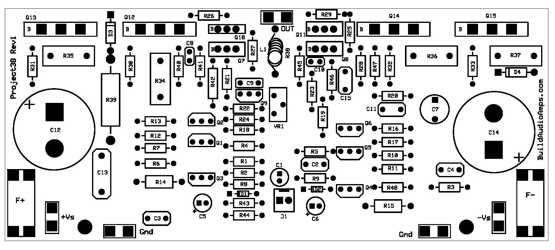 Project 38 Silkscreen Parts Placement Layer of PCB.
If you’ve decided to build this project, the idle current needs to be adjusted first before going any further. Insert a jumper or shunt at the input of the amplifier. Do not connect any load or loudspeaker at the output of the amplifier. Adjust VR1 for maximum resistance of 1KΩ; please refer to the schematic diagram where to access VR1 on top of PCB. Prepare 3 DMMs to measure the DC offset voltage at the output of the amplifier, the voltage drop of the emitter resistor in any of the power output transistors, Q12 through Q15 and the overall current across the F+ fuse terminals. It is highly recommended to use a Variac transformer when performing the initial test of the project. If something goes wrong with the project, minimal damage will occur to the components or just a blown fuse. However both test procedures with or without the use of a Variac transformer will be explained.
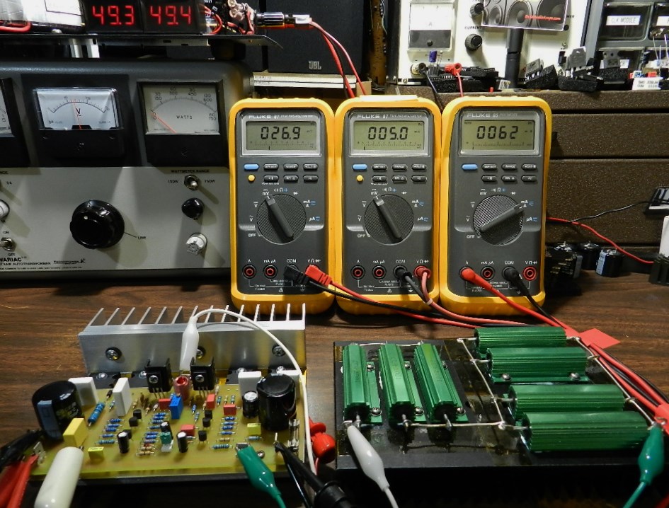
If a Variac transformer is available, connect the AC input of the power supply to the output of the Variac transformer. Switch the power to ON and gradually adjust the Variac’s AC output from zero until the voltage output of the power supply reaches approximately ±49VDC to ±55VDC while observing for sudden increase in any DMM readings. If you have encountered an unusual increase in any of the DMM readings, switch the power to OFF immediately and check the PCB for assembly errors. The picture above shows a DC offset voltage at 26.9mV. The voltage drop across any emitter power resistor is about 5mV; readjust VR1 to get a DMM reading from 5mV to 10mV after 10 minutes of warm-up time. The current across the F+ fuse terminals is 62mA; this value is dependent on the adjustment of VR1 and could be from 60mA to 120mA. If you obtain similar DMM readings, you may proceed with music test.
If a Variac transformer is unavailable, make sure that the power supply was properly built and that the output voltage rails have been measured at approximately ±49VDC to ±55VDC before connecting it to the amplifier project under test. With the power supply switched to OFF, adjust VR1 for maximum resistance. Switch the power supply to ON; the DMM measuring the voltage drop across any emitter power resistor should read less than 1mV. If the DMM reading is more than 1mV and cannot be adjusted by VR1, power OFF immediately and check the PCB for assembly errors. If the DMM reading is less than 1mV, adjust the reading from 5mV to about 10mV after 10 minutes. The DMM that is connected across the F+ fuse terminals will read about 60mA to 120mA of total current. If you obtain similar DMM readings, you may proceed with music test.
The next test procedure is optional, but if an oscilloscope, audio signal generator and 8Ω dummy load are available, the maximum power output before clipping can be measured. Be careful not to touch the project’s heatsink and dummy load, it will get very hot during this test.
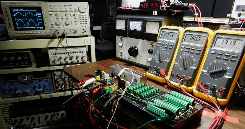
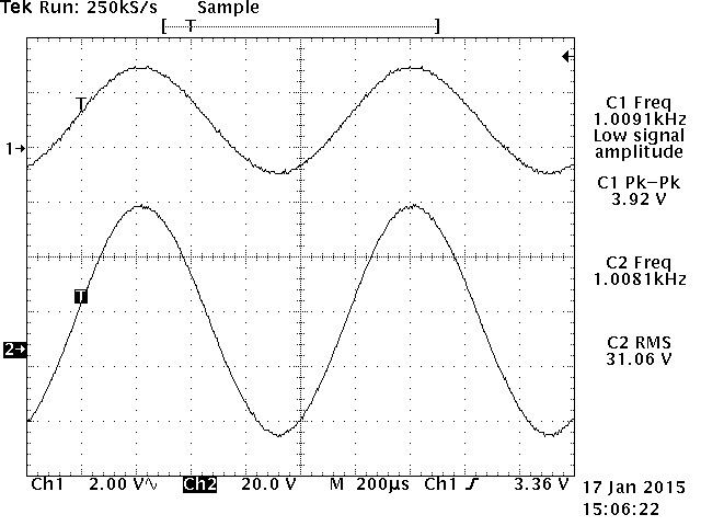
The power output was measured using an HP3312A Function Generator set at 1KHz 3.92Vp-p sine wave output and connected directly to the input of the amplifier under test as well as the CH1 test probe of the oscilloscope. An 8Ω/700Watt dummy load was connected at the output of the amplifier under test as well as the CH2 test probe of the Tektronix TDS520D 500MHz DPO. The power amplifier produces a very nice sine wave of 31.06Vrms across the 8Ω/700W dummy load or a power output of about 120 Watts, as shown in the TEK hardcopy pictures above. The oscilloscope’s horizontal scale was adjusted at 200uS to verify for any visible clipping or artifacts on either peak. This project was paired with a modified PreAmp1 tone control project; the audio quality reproduced was excellent.
![]()