Project 47

Project 47 is another CFA-based 100-watt at 8Ω or 200-watt at 4Ω audio power amplifier project. The project’s prototype achieved a 100KHz square wave rise time of 245.1nS and a 200KHz square wave rise time of 244.2nS, shown in the Tek hardcopy pictures below. Both square wave signals were adjusted at approximately 28Vpp with insignificant overshoots on both peaks. These measurements correspond to a slew rate of 359V/uS for the 100KHz and 360V/uS for the 200KHz square wave signals.
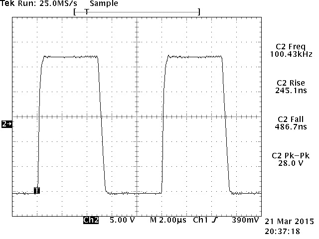
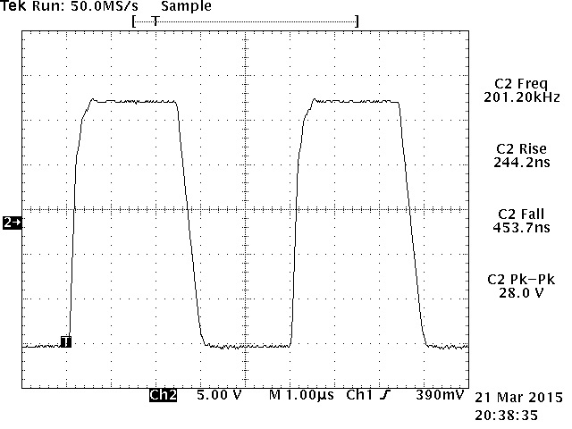
100KHz square wave rise time measurement. 200KHz square wave rise time measurement.
The power output before clipping was measured by applying a 1KHz sine wave signal with the amplitude adjusted at 3.12Vpp (1.103Vrms) to the input of the amplifier, J1. The amplifier produces 28.79Vrms across the 8Ω dummy load connected at the output of the amplifier. The Tek hardcopy pictures below show the power output at 77watts (Vin=2.72Vpp) and just before clipping at 104watts.
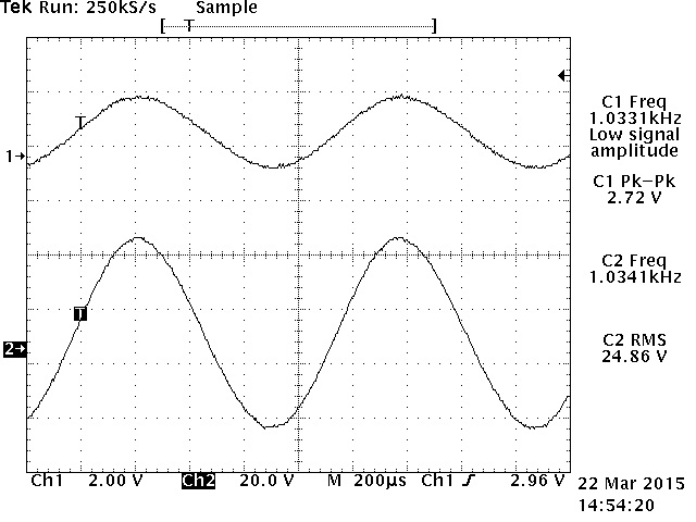
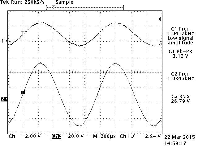
Power output measured at 77 watts 8Ω. Power output measured at 104 watts 8Ω.
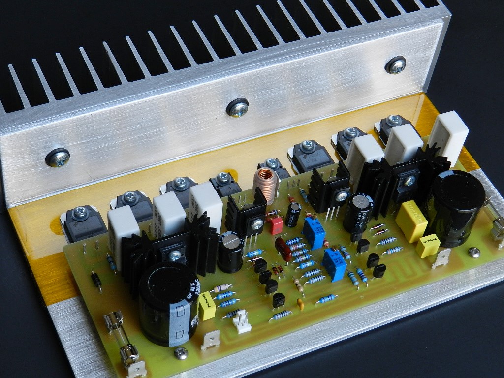
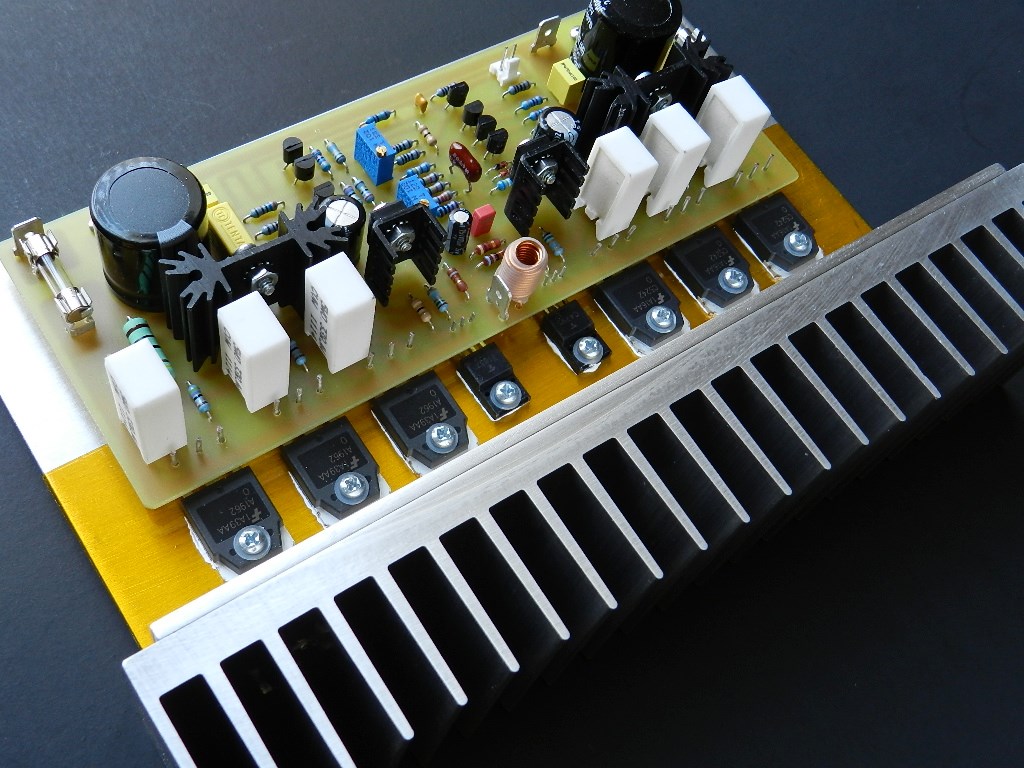
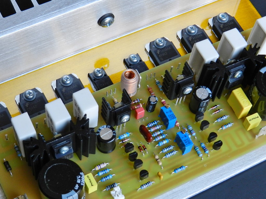
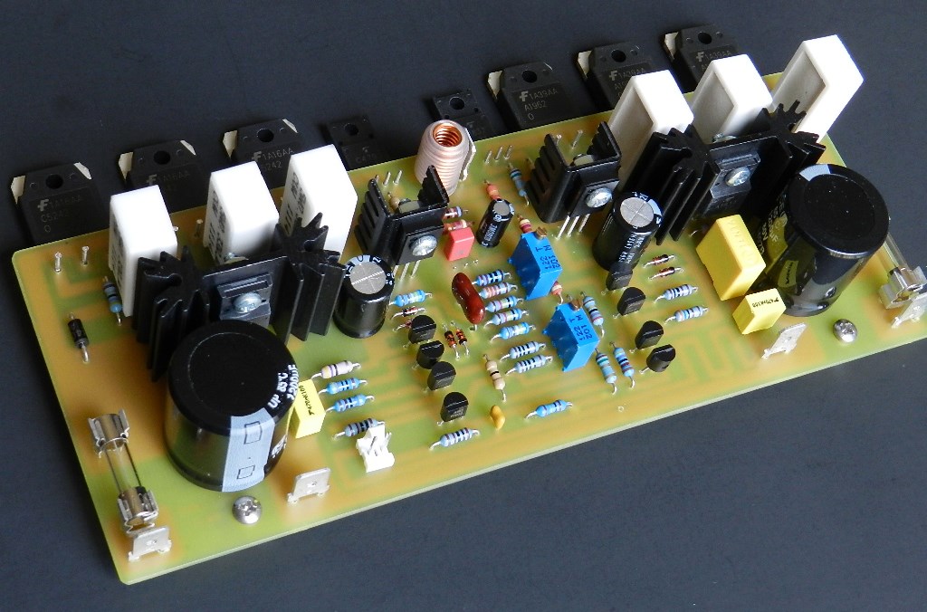
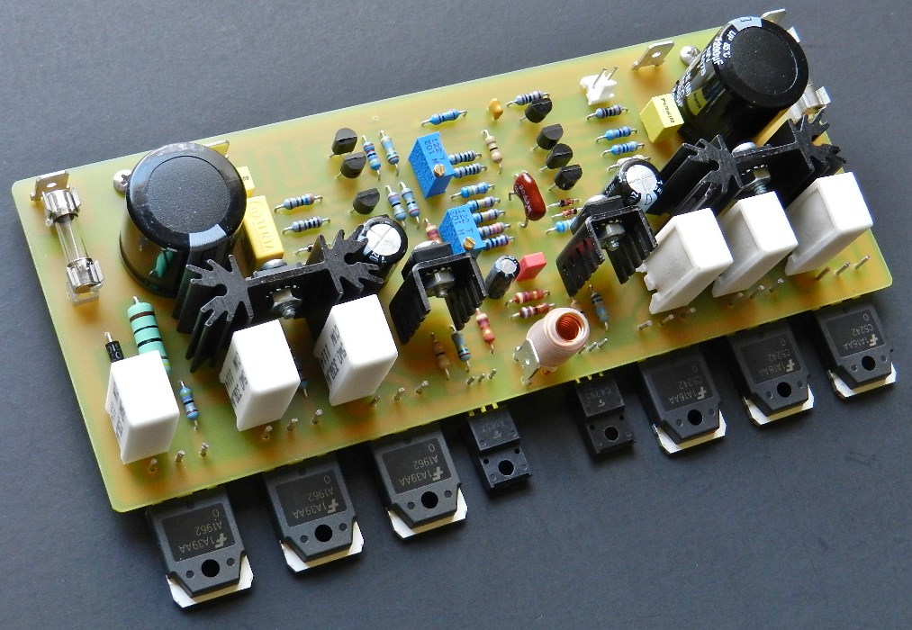
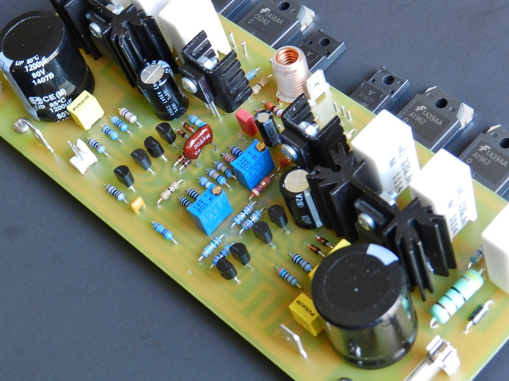
The prototype model was built on a 7.25” X 2.8” single-sided PCB. All components used in the prototype are readily available standard parts. If you are interested in building this project and have read the Information and Policies section of this website, the schematic diagram, PCB layout (available only by request) and BOM are free, as is, no warranty.
 Project 47 Silkscreen Parts Placement Layer of PCB.
Please refer to the schematic diagram for a brief description of the circuit. The input signal at J1 is directly coupled and passes through a low pass filter consisting of R1 and C1 that suppresses unwanted RF noise from entering the complementary emitter-follower buffer stage transistors, Q1 and Q2. R2 supplies the base bias for Q1 and Q2 and its chosen value also reduces the overall DC offset voltage of the amplifier to minimum. Q1 and Q2 are loaded with JFET current source transistors, Q3 and Q4. The output of the buffers drives the summing stage transistors, Q5 and Q6. A feedback node consisting of R8 and R9 in parallel with VR1 sets the overall DC offset voltage of the amplifier by ±200mV. If optimum DC offset voltage is desired, an integrator op-amp similar to the one used in Project 4 can be implemented. Negative feedback resistors, R11, R10, R21 and R24 are also connected in that same feedback node. These resistors determine the overall gain of the amplifier at 26dB.
The output of Q5 is connected to a cascode circuit consisting of transistors, Q8 and Q9. Q9 is biased by series connected small signal diodes in parallel with a filter capacitor, C3, which helps stabilize the voltage across the diodes. Another JFET current source, Q7, is connected between the bases of Q9 and Q10. A VBE circuit consisting of Q11, VR2 and other associated components is connected between the collectors of transistors, Q9 and Q10. This circuit sets the zero bias of the power output stage transistors. The overall front-end stage output is taken from the collectors of transistors, Q9 and Q10 and frequency compensated by capacitor, C2.
The amplifier is outfitted with a triple emitter-follower power output stage. Pre-driver transistors, Q12 and Q13, isolate the output of Q9 and Q10 from the main driver transistors, Q14 and Q15. Utilizing three pairs of paralleled complementary power output transistors, Q16 through Q21, allow the amplifier to drive low impedance loads.
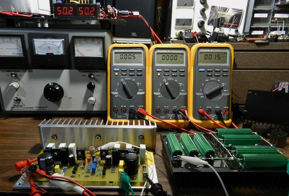
The amplifier requires approximately ±50VDC power supply rails; produced from a rectified and filtered 70VCT at 200 or 300VA power transformer. The picture above shows digital panel voltmeters reading of ±50.2VDC, obtained by connecting the AC input of the power supply to the AC output of the Variac transformer. The initial testing of the prototype requires three DMMs connected to: the output of the amplifier, across the emitter resistors R33/R36, and at the F+ fuse terminals. The DMM on the left side of the picture above is measuring the DC offset voltage at 0.5VDC, which can be set by adjusting VR1. The DMM in the middle measures 0V across emitter resistors, R33 and R36; this can be acquired by adjusting VR2. The DMM on the right side of the picture is measuring the overall current across the F+ fuse terminals at 15mA, which is dependent on the adjustment of VR2.
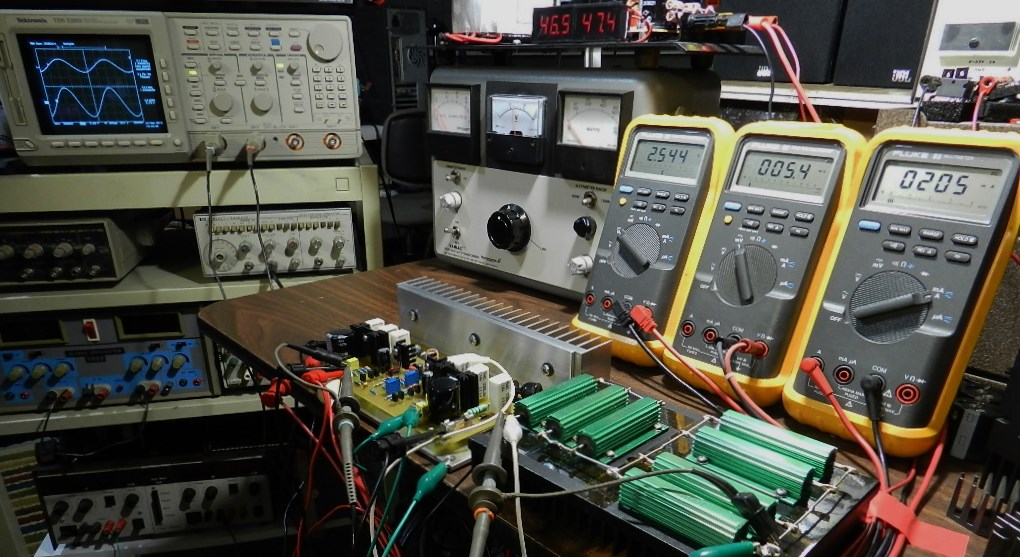
The picture above shows the test setup for power output and slew rate measurements. An HP3312A function generator and a Tektronix TDS520D 500MHz oscilloscope was used for these particular tests. However, similar equipment can be used if you’re planning to perform the same optional tests. Be careful not to touch the amplifier under test, heatsink and dummy load; they will get extremely hot. The dummy load is only connected to the amplifier during initial testing and power output measurement. It should be disconnected from the output of the amplifier in slew rate measurement. The Zobel network resistor, R38 (a 10Ω 3W wire wound power resistor), should be disconnected as well. Running a continuous 100KHz and 200KHz square wave signal to the amplifier will destroy this resistor.
In real world listening with various music materials, the experience was extraordinary. The prototype unit was connected to a modified LM49720 tone control preamp. Listening to Holly Cole’s “Train Song” and “Jersey Girl” from her “Temptation” album, played on a Toshiba HD-A2 player and a Kenwood MV-9D monitor speaker, you hear impressive clarity in the entire audio frequency spectrum. Brian Bromberg’s outstanding solo bass performance on tracks 3, 7 and 10 from his “Wood II” album was also played. The entirety of John Patitucci’s “Imprint” album was also auditioned for endurance music testing.