Project 31
The concept for this project is based on a complementary-symmetrical differential input stage circuit popularized in the Hafler DH-200 stereo amplifier kit in the 70’s designed by Erno Borbely, which he named the double differential input amplifier. The Audionics CC2 amplifier created by R. L. Sickler uses the same full complementary-symmetry topology originated from Fairchild’s application notes. The input stage topology was also used by G. R. Slone, in his quest for the optimum audio power amplifier design and appropriately named it as the mirror-imaged input stage topology. The same topology was also used as well in the Low TIM Amp, also known as the Leach Amp designed by W.M. Leach, Jr.
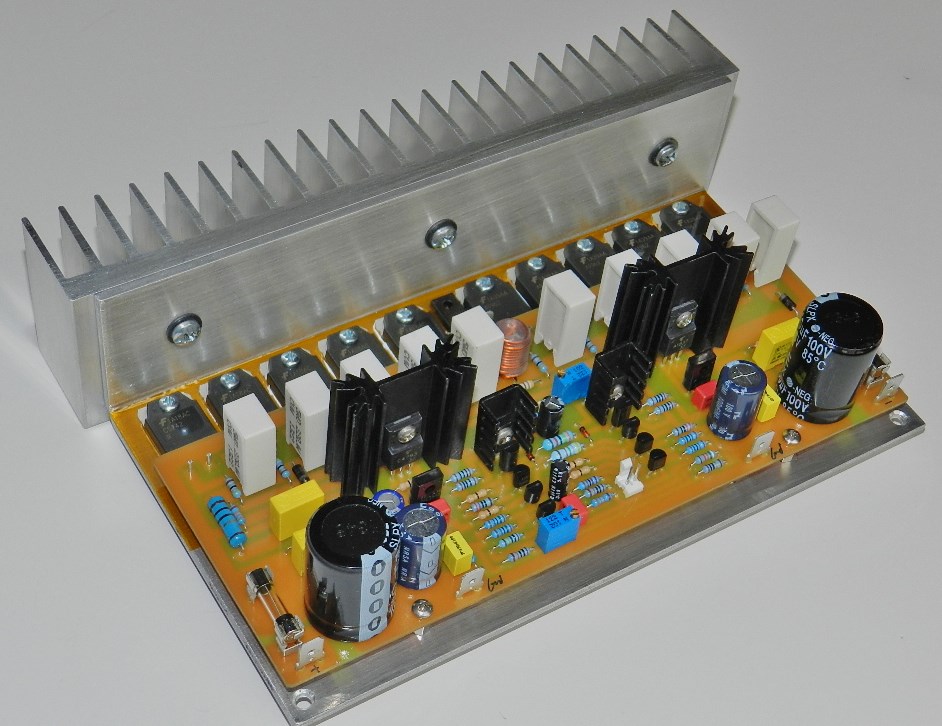
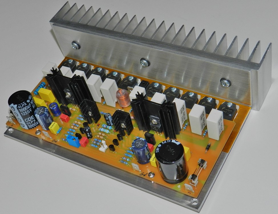
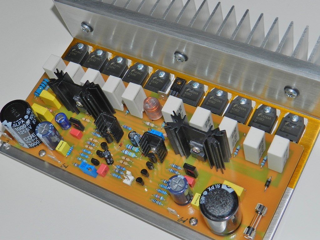
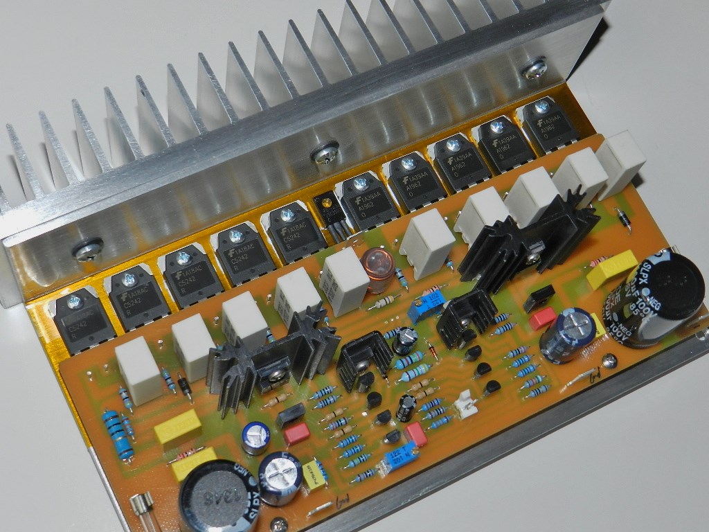
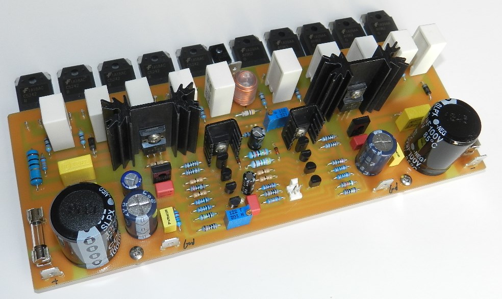
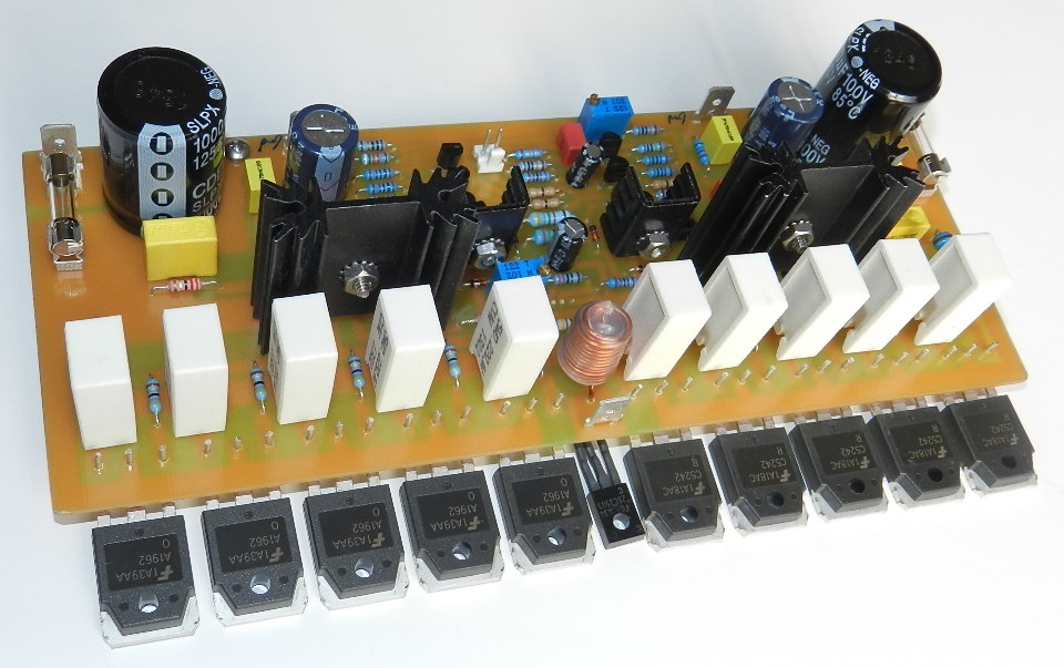
Project 31 features a similar input stage topology consisting of complementary symmetrical differential input amplifier, current source and voltage amplifier stages. The input signal is connected simultaneously to the bases of the complementary differential input stage amplifiers. A portion of the output signal is feedback similarly to the inverting inputs of the same differential amplifiers. The current sources for each differential pairs are also complementary as well as the voltage amplifier stages. With this push-pull type of topology, the DC offset voltage should be very low compared to other topologies, but VR1 is added at the base of Q1 and Q9 to conveniently trim this voltage to minimum. The output stage is the usual three-stage emitter-follower circuit that have been used in several projects presented here in this website. The measured power output of this project before clipping occurs is 233Wrms into an 8Ω load with ±65VDC power supply rails.
The audio quality reproduced by this topology type is surprisingly excellent. If you plan to create your own PCB layout, the ground trace of input J1 must be laid out farther away from the main power ground trace. A 10Ω resistor was also added in series with J1 and power supply ground. This will lift the input ground from main ground, labeled 0V in 2 places, as shown in the silkscreen layer of PCB below. If you are interested in building this project and have read the Information and Policies section of this website, the schematic diagram, PCB layout (available only by request) and BOM are free, as is, no warranty.
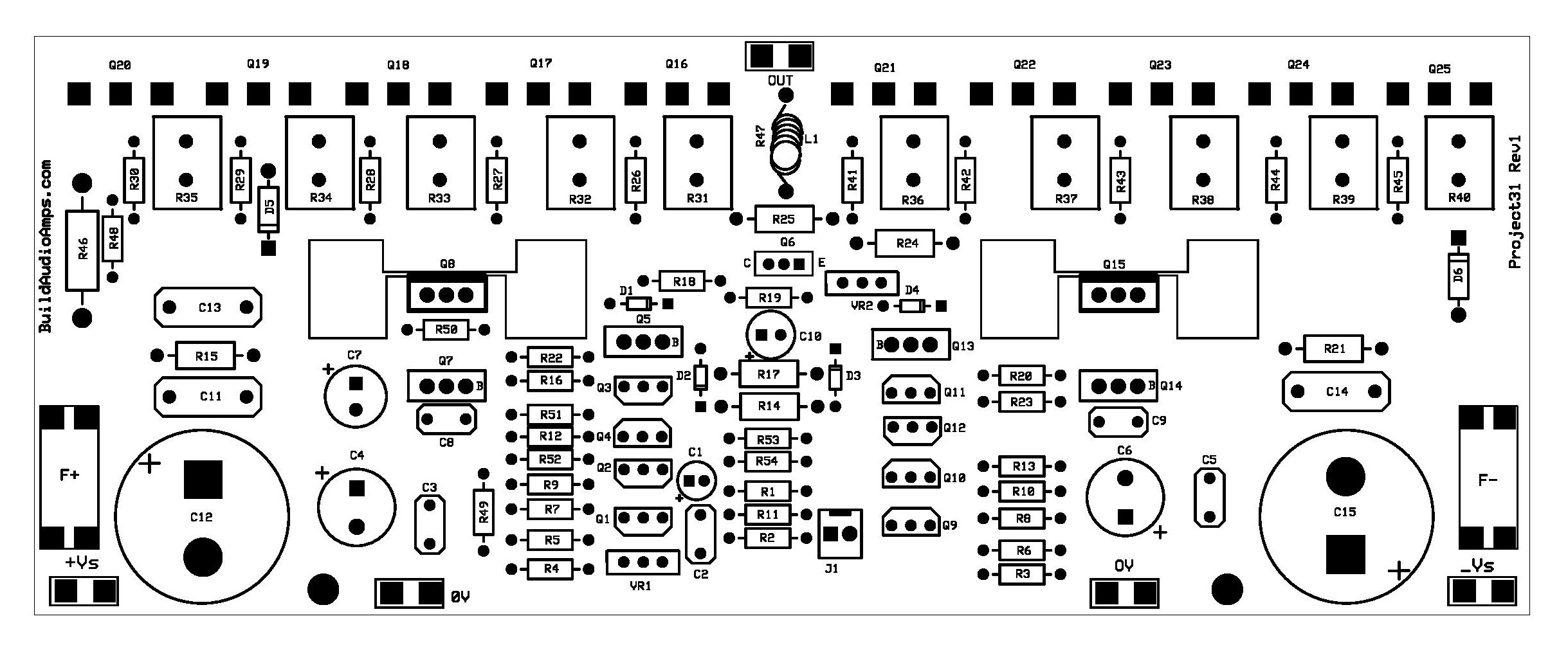 Silkscreen Parts Placement Layer of PCB for Project 31.
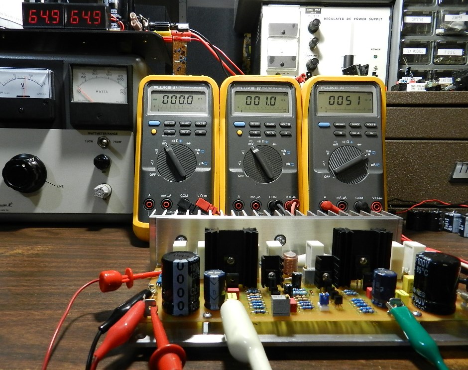
If you’ve decided to build this project, the DC offset voltage and the idle current needs to be adjusted first before going any further. Insert a jumper or shunt at the input of the amplifier. Do not connect any load or loudspeaker at the output of the amplifier. Adjust VR2 to maximum resistance of 5KΩ; please refer to schematic diagram where to access VR2 on top of PCB. Prepare 3 DMMs to measure the DC offset voltage at the output of the amplifier, the voltage between the emitters of Q20 and Q25 power output transistors and the current across the F+ fuse terminals. Experienced amp builders have more than 3 DMMs.
If a Variac transformer is available, connect the AC input of the power supply to the output of the Variac transformer. Switch the power to ON and gradually adjust the Variac’s AC output from zero until the voltage output of the power supply reaches approximately ±64VDC while keeping an eye on sudden increase in any DMM readings. If you have observed an abrupt increase in any of the DMM readings, switch the power to OFF immediately before any populated component vaporizes and check the PCB for assembly errors. The picture above shows a DC offset voltage at 0.0mV; adjust VR1 to get to this value. The voltage across Q20 and Q25 is measured at 1.0mV after a warm-up period of 10 minutes; readjust VR2 to get a DMM reading from 1mV to 3mV. The current across the F+ fuse terminals measured at 51mA, this value is dependent on the adjustment of VR2. If you obtain similar DMM readings, you may proceed with music test.
If a Variac transformer is unavailable, make sure that the power supply has been properly built and that the output voltage rails have been measured at approximately ±64VDC before connecting it to the project. With the power supply at OFF, adjust VR2 for maximum resistance. Switch the power supply to ON; the DMM measuring the voltage across Q20 and Q25 should read less than 1mV. If the DMM reading is more than 1mV and cannot be adjusted by VR2, power OFF immediately and check the PCB for assembly errors. If the DMM reading is less than 1mV wait for 10 minutes and carefully adjust the reading from 1mV to 3mV. Adjust the DC offset voltage thru VR1 for minimum or within ±10mV DMM reading at the output of the amplifier. If you obtain similar DMM readings, you may proceed with music test.
The next test procedure is optional, but if an oscilloscope, audio signal generator and 8Ω dummy load are available, the maximum power output before clipping can be measured. Be careful not to touch the heatsink or the dummy load during this test, they will get very hot!
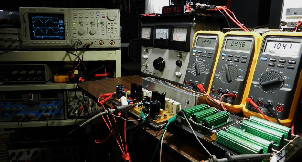
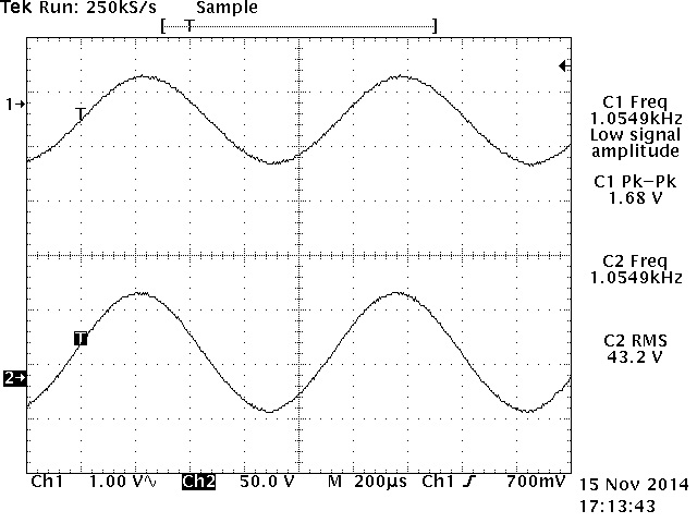
The power output was measured using an HP3312A Function Generator set at 1KHz 1.68Vp-p sine wave output and connected directly to the input of the amplifier under test as well as the CH1 test probe of the oscilloscope. An 8Ω/700Watt dummy load was connected at the output of the amplifier under test as well as the CH2 test probe of the Tektronix TDS520D 500MHz DPO. The amplifier project produces 43.2Vrms across the 8Ω/700W dummy load or a power output of about 233Wrms, as shown in the TEK hardcopy picture on the right. The oscilloscope’s horizontal scale was adjusted at 200uS to verify for any visible clipping or artifacts on either peak. This project was paired with Project 9, the LM1036 tone control project. This project was also tested at ±45VDC power supply rails, although power output have been reduced the audio quality reproduced did not disappoint.