Project 63


Project 63 is the second in the series of audio power amplifiers in which a low-noise high-speed JFET input operational amplifier is used at the front-end input stage of the amplifier. So far, there are more than eight similar projects that have been developed for this series. The specified op-amp in this project, which is ideally suited for high fidelity audio application, provides the necessary gain for the voltage and current feedback modes of amplification. The combined negative feedback types that were implemented into this project reproduced superb audio quality and performance. However, prior to this project, several op-amp based audio power amplifier circuits have been experimented, built and literally sound great but have limited measured power output mainly caused by the op-amp’s inability to provide higher output greater than its power supply rails. To overcome this limitation it is necessary to add a voltage amplifier stage or use the suspended supply regulator method.
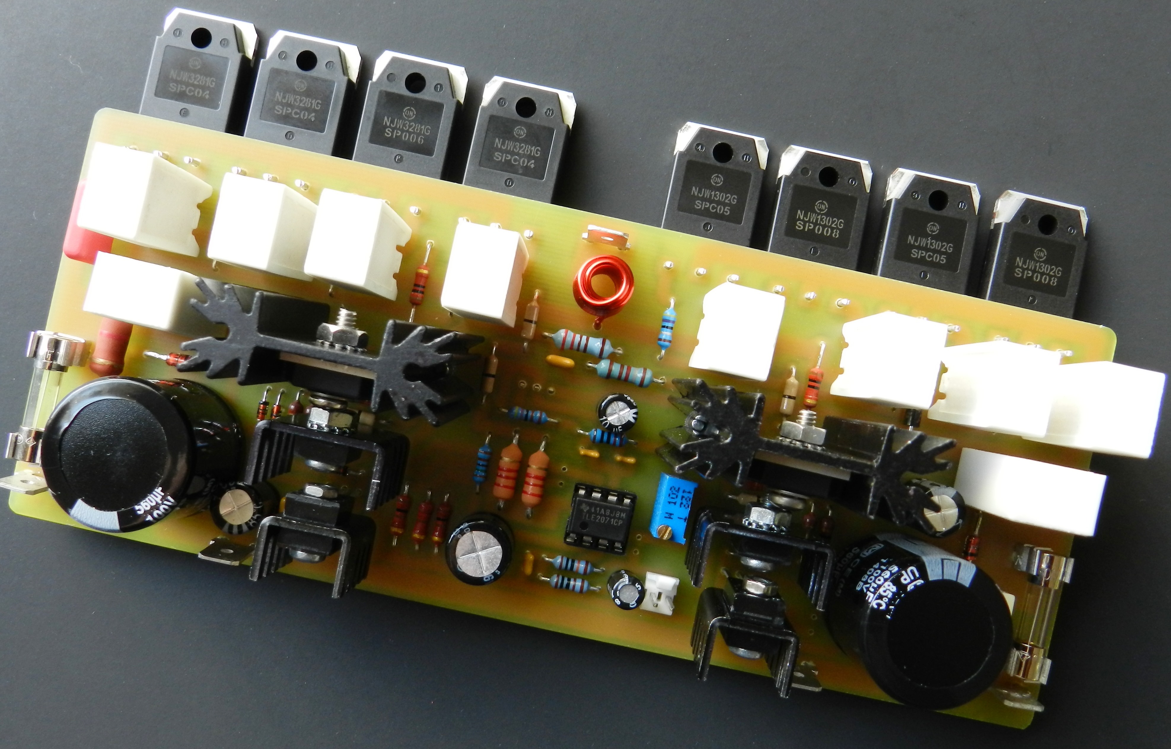
The three-stage emitter-follower configured power output stage connected to a ±60VDC power supply, delivers an unclipped power output of about 214 watts into an 8Ω load with a THD of 0.00157% as measured by a QA400 audio analyzer. By using four complementary pairs of highly reliable 15A 250V 200W silicon power transistors from On Semiconductor, higher power output may be realized especially when connected to very low impedance loads.
A very interesting feature of this amplifier project, as mentioned earlier, is the combination of the voltage and current negative feedback network connected at the inverting input, pin2, and the output of the op-amp, pin 6, respectively. The current output signals are taken from the power supply rail pins of the op amp, similar to the Alexander current feedback amplifier design. However, the difference in the latter design with this project is the introduction of a voltage feedback signal at the inverting input of the op-amp. Both negative feedback resistor networks functions harmoniously courtesy of R8, please refer to the schematic diagram from hereon.
If an input signal is applied to the non-inverting input of the op-amp, pin3, this forces to increase the current at R14 through feedback resistors, R15 and R16. The increase in current across this low impedance load causes a proportional increase in the current at pins 4 and 7; it is then converted to voltage by Q3 and Q4 and loops as long as the input signal is present. A small ratio of the voltage coming from the main output of the amplifier is applied into the inverting input of the op-amp, pin 2, by way of the voltage feedback network consisting of R6, R13 and C9. The same output signal of the amplifier is applied into the low impedance current feedback network consisting of R14, R15 and R16 and into the output of the op-amp, pin 6. Series-pass regulators Q1 and Q2 are voltage referenced by D1 and D4 at approximately ±15VDC. It is enticing to add decoupling capacitors at pins 4 and 7 of the op-amp as experienced during development, but in square wave response testing this causes severe overshoots and noise in both amplitudes regardless of frequency. Leave it as it is in its pristine desired condition.
The required bias of the power output stage is provided by Q17 along with its associated components. One terminal of each frequency compensation capacitors, C7 and C8, are connected at the current feedback node i.e. the output of the op-amp, pin 6, while their other terminals are connected to the collector and emitter of Q17. The measured voltage drop across R11 and R12 of Q3 and Q4 respectively is about 0.156V or a current flow of about 2.3mA. There is about 2.5V across each emitter of the buffer driver transistors, Q5 and Q6. About half a volt is measured across R21 and R22 of the driver transistors, Q7 and Q8. R21 and R22 are rated at 1 watt as populated in the prototype and have been simulated to determine its minimum wattage which breaks/opens if 3 volts is exceeded between the bases of Q7 and Q8. However, you may substitute it with a small footprint 2-watt flameproof type instead. Although Q7 and Q8 can dissipate about 130 watts of power, it still needs a medium-sized extruded heat sink similar to the Aavid Thermalloy P/N 513202B02500G to cool it down to about 55°C, that’s about less than half of its rated operating junction temperature or a derated power dissipation of about 90watts. The only protections included in the amplifier are D7, D8 and the ± rail fuses but the updated uPC1237 Speaker Protection and Power ON Delay Project may easily be added for peace of mind.
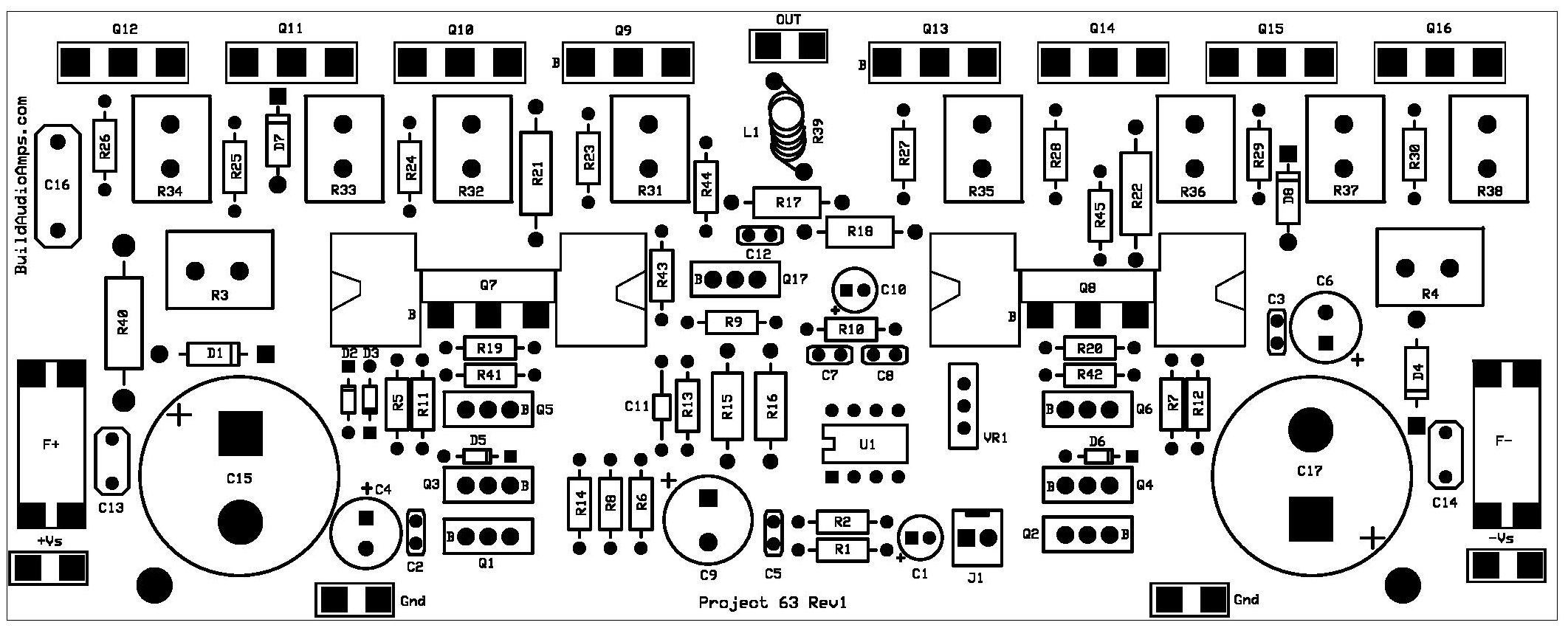
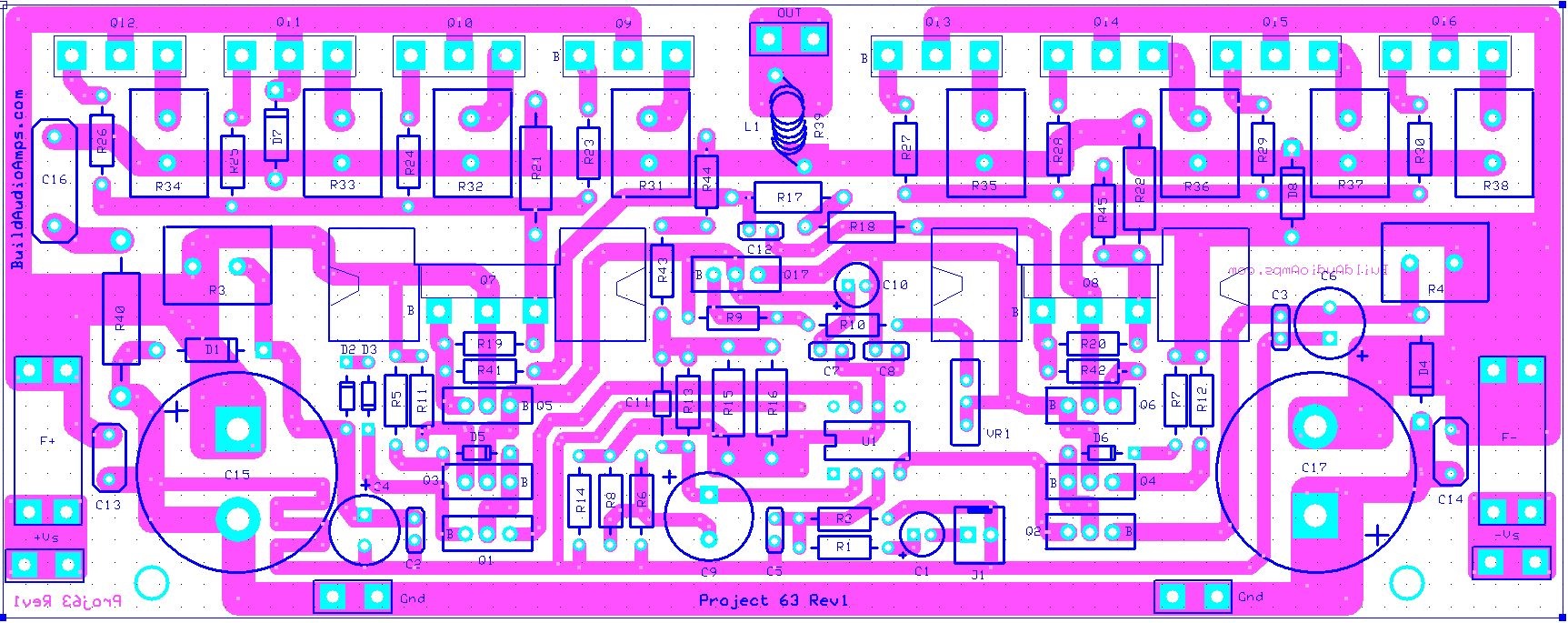
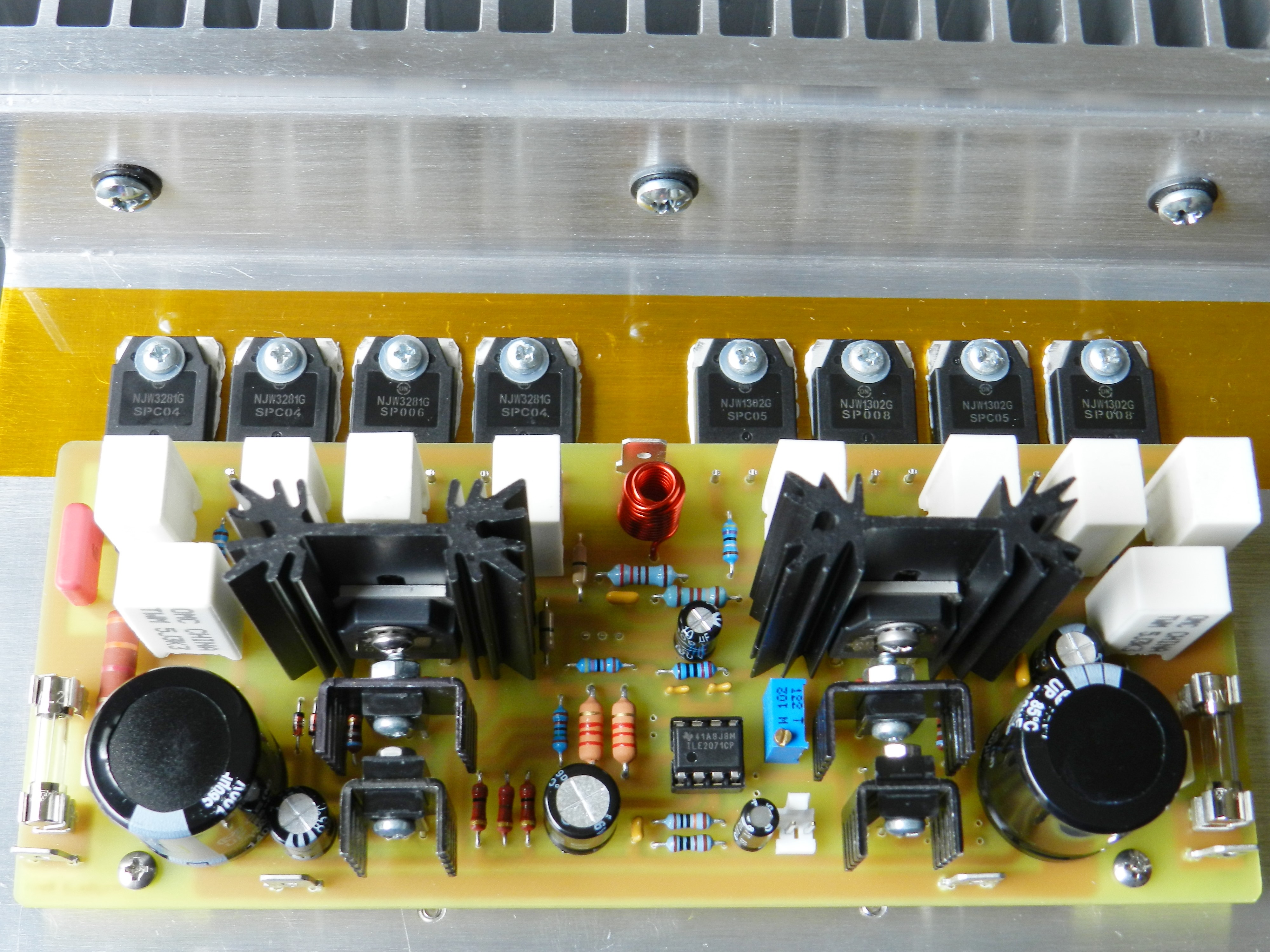
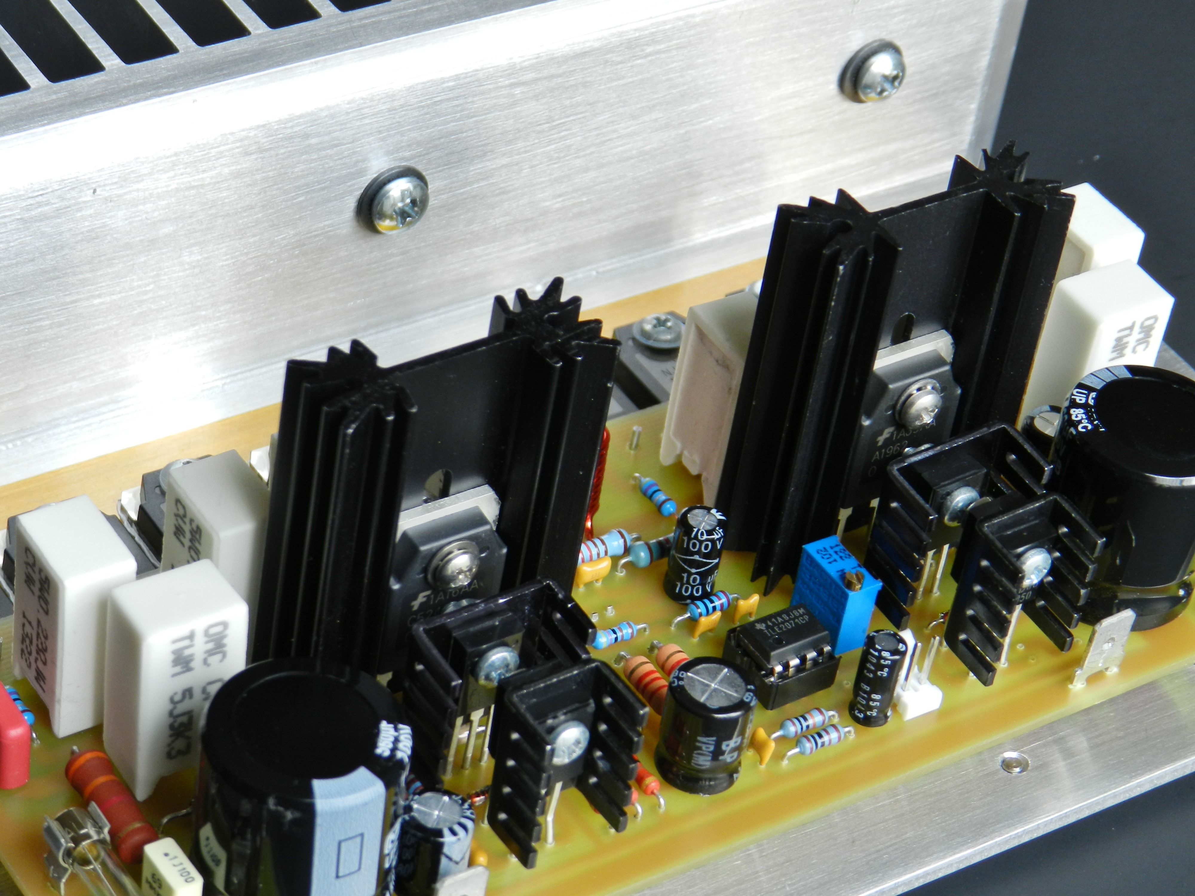
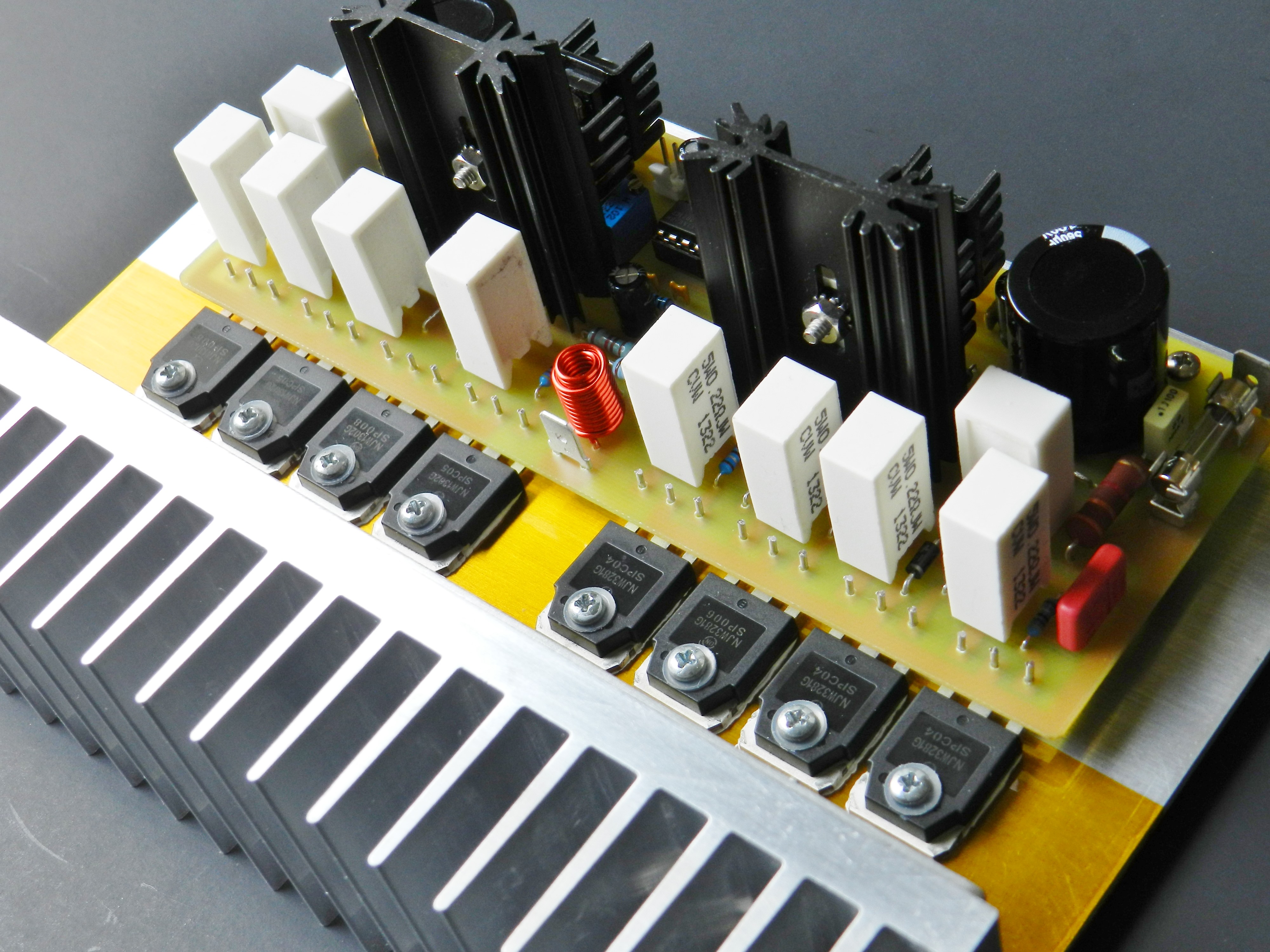
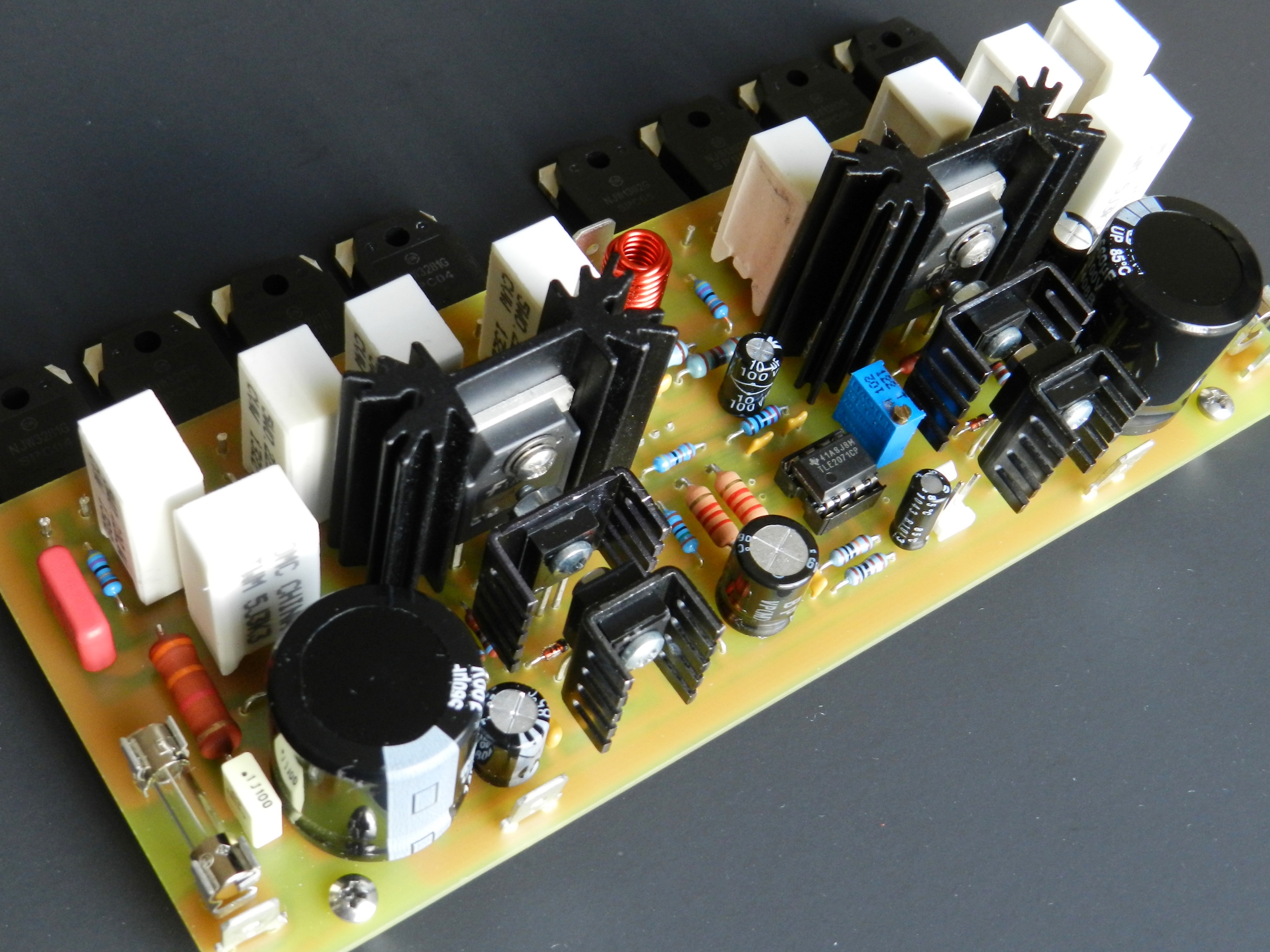
Figure 1a. Silkscreen parts placement layer of the PCB. Figure 1b. Detailed parts placement and copper layers of the PCB.
The prototype’s PCB layout was created using ExpressPCB software, laser printed and etched into a 7.00” X 2.75” single-sided copper board as shown in Figures 1a and 1b. If you are creating your own PCB, Figure 1b will serve as a model for the suggested routing and sizing of the copper traces. PCB layout is critical for this type of topology. The header and bottom pictures on this page show the completed prototype of Project 63. The PCB layout and BOM are free to registered users only and available only by request, as it is, no warranty whatsoever.
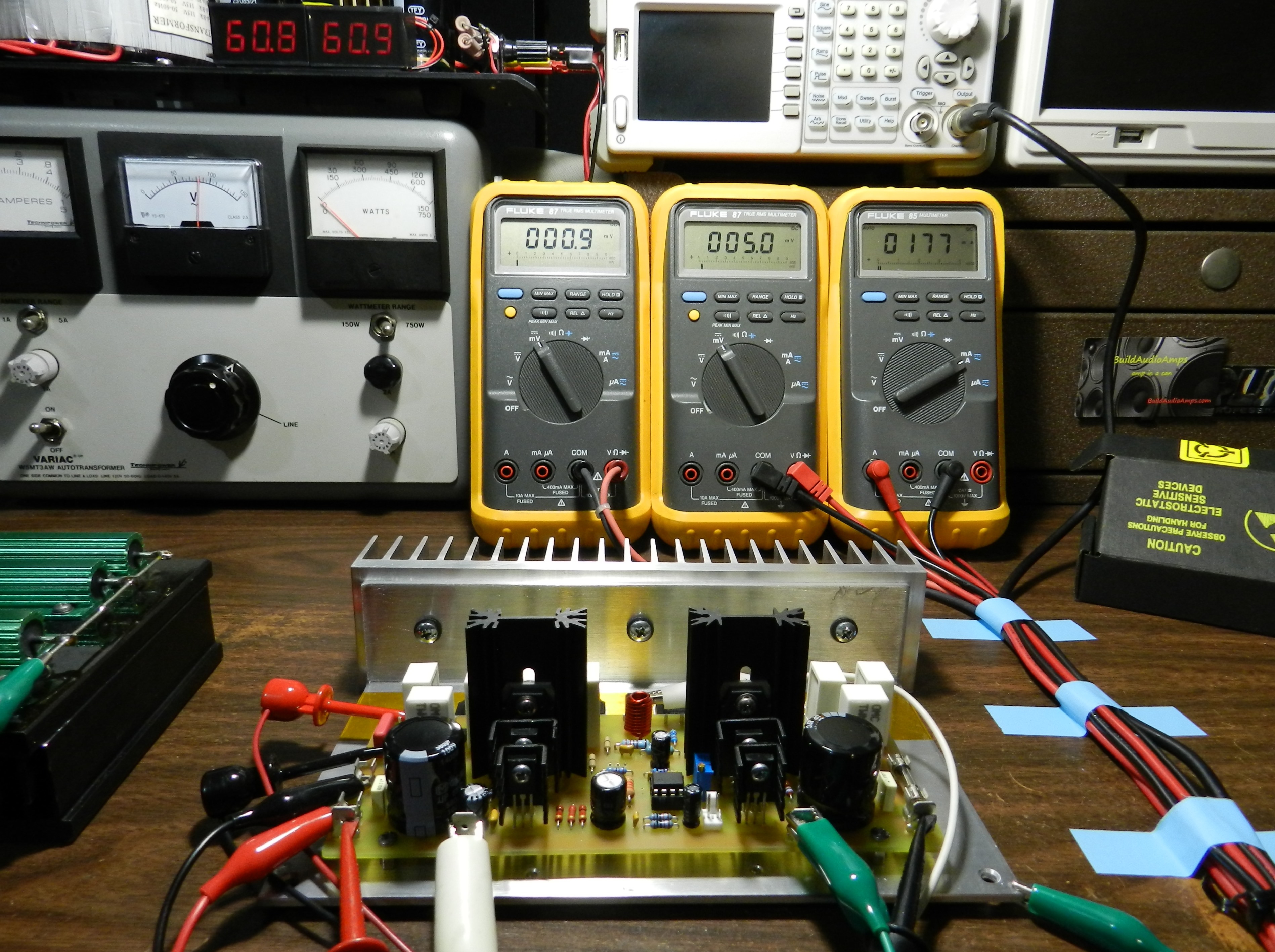
Figure 2. Initial test DMM readings and setup.
The initial test setup of Project 63 is shown in Figure 2. The prototype is powered with ±60VDC rails from a rectified and filtered 42V-0-42V 400VA power transformer similar to AnTek AS-4442 or AN-4242 toroidal power transformers. When power is applied to the amplifier, be sure not to touch the extruded heat sink of the driver transistors at the same time, there is a total of 120VDC between them. Q7 and Q8 are T03-P packaged and have non-insulated collector metal tabs.
The DMM on the left is connected at the output of the amplifier and measures the DC offset voltage at 0.9mV. The DMM in the middle is connected across the emitter resistor, R34, of the power output transistor, Q12. The DMM measures 5.0mV across R34 or a bias current of about 22.7mA. This was acquired by adjusting VR1 after a warm-up period of about 15 minutes or more. This voltage may be adjusted to a minimum of 1mV without sacrificing the audio quality and having the advantage of much cooler power transistors. The DMM on the right is connected across the F+ fuse terminals and measures the total current drawn by the amplifier at 177mA. This reading is dependent on the adjustment of VR1.
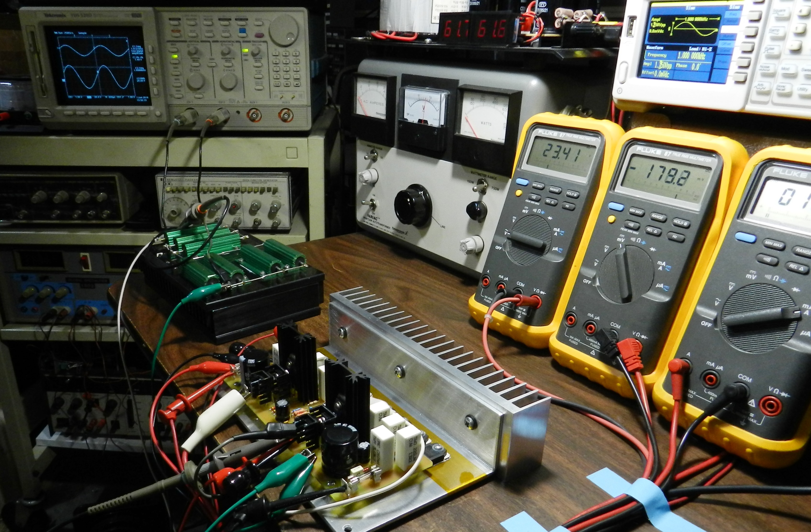
Figure 3. Power output and square wave response test setup.
Figure 3 shows the test setup for power output and square wave response tests. This test is optional; you may proceed to music listening test if you have performed the previous test. The power output test stresses the amplifier to its limits and needs your utmost attention if you are planning to perform this test. An oscilloscope, function generator and an 8Ω dummy load are required for these tests. In the power output measurement, the function generator is set to produce a sine wave output of 1KHz with the starting amplitude at 100mV. Connect this signal to J1 as well as CH1 probe of the oscilloscope. The 8Ω dummy load and CH2 of the oscilloscope are connected at the output of the amplifier. Adjust the amplitude of the 1KHz sine wave input signal until it barely reaches clipping as shown in Figure 4a. The maximum input signal of 2.88Vpp was determined to produce a 41.34Vrms across the 8Ω dummy load or a power output of about 213.62 watts. Figure 4b shows a symmetrical clipped output waveform when the input signal was increased to about 3.04Vpp.

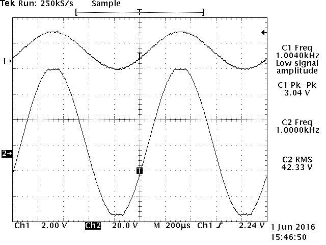 Figure 4a. Power output test result before clipping. Figure 4b. Power output test result at clipping.
The 20Hz, 1KHz, 20KHz and 100KHz square wave response test results are shown in Figures 5a through 5d, respectively. The function generator on this test was set to produce a square wave output of the desired test frequency. The amplitude was then adjusted so that the output waveform does not show any signs of overshoots on its peaks. The oscilloscope is set with CH1 trigger but its waveform is OFF, this allows you to display only CH2 as shown in the following Tek hardcopy pictures in Figures 5a through 5d.
During initial square wave response testing using only one complementary pair of output power transistors, an overshoot was noticed at the positive half of the waveform. A quick fix is to add a small capacitor about less than 50pF in parallel with R13. However, when the PCB was fully populated (four pairs) this artifact went away completely without the need of adding a negative feedback capacitor.
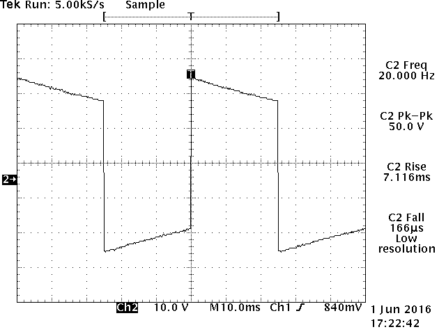
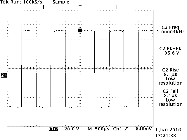 Figure 5a. 20Hz square wave response test result. Figure 5b. 1KHz square wave response test result.
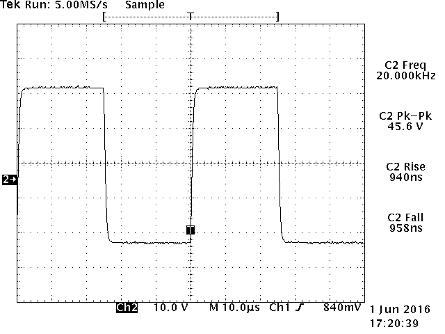
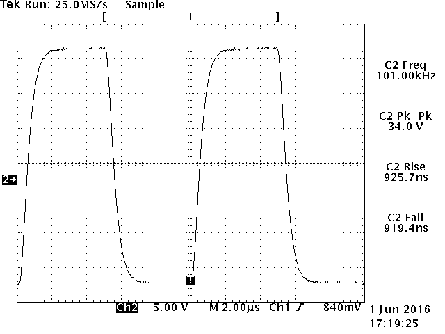 Figure 5c. 20KHz square wave response test result. Figure 5d. 100KHz square wave response test result.
One of the easiest and economical way of measuring THD, Noise, SNR and frequency response with acceptable test results is to use QuantAsylum’s QA400 USB powered 192Ksps 24-bit stereo audio analyzer with the QA190 differential probe. The QA190 allows you to measure directly the output signal of the audio amplifier and at the same time protects the low-level input of the QA400. Although, QuantAsylum have released their second generation of audio analyzer, but with no foreseeable revenue for BuildAudioAmps.com, the QA400 will suffice at this time to show the measured performance of built audio amplifier projects.
Figure 6 shows Project 63’s test setup of measuring its basic performance parameters. Figure 7a shows the test result for noise, THD, THD+N and SNR while Figure 7b shows a flat frequency response test result of the amplifier.
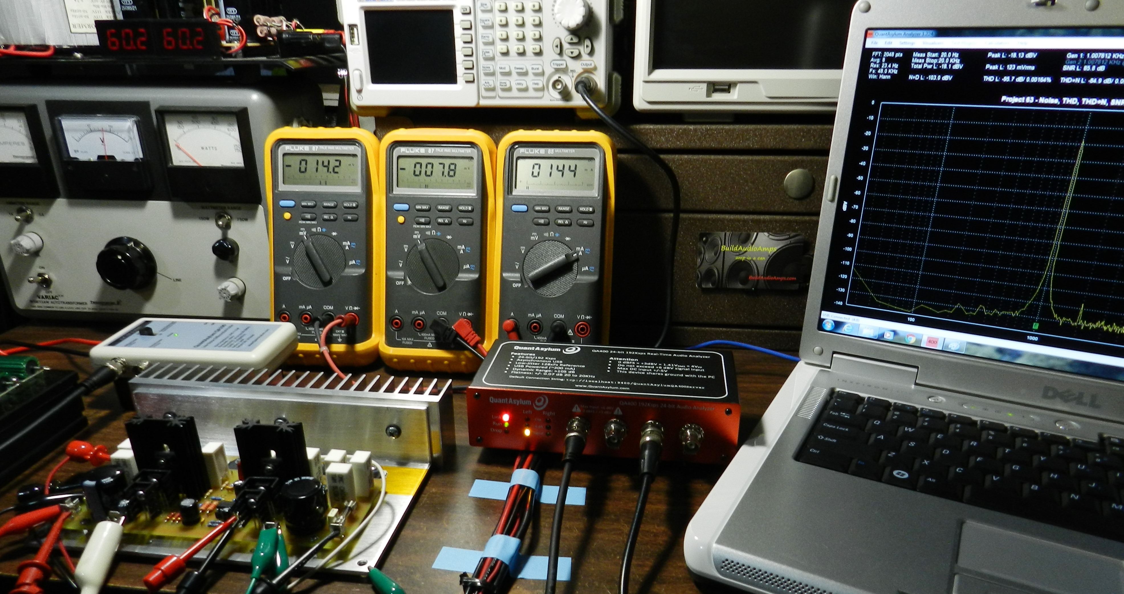
Figure 6. QuantAsylum’s QA400 test setup for Project 63.
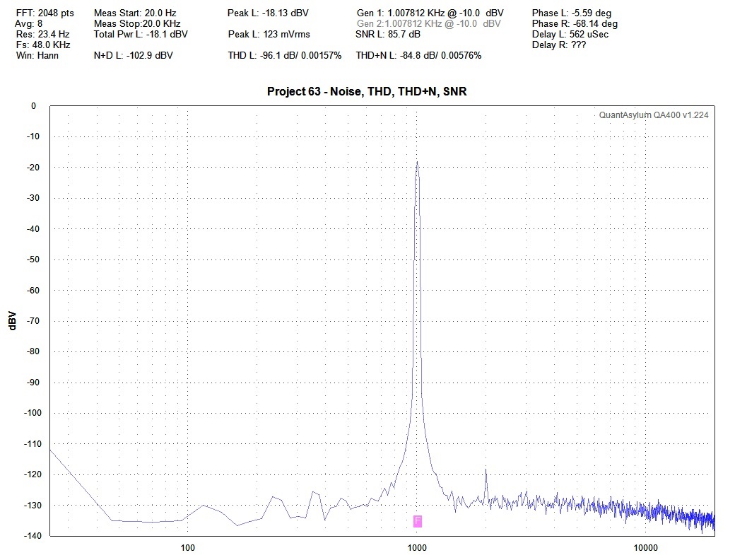
Figure 7a. QA400 test result for Noise, THD, THD+N and SNR measurements.

Figure 7b. QA400 test result for Frequency Reponse measurement.
How does it sound? The prototype unit was connected with a modified LM49720 tone control preamp, Toshiba HD-A2 player and several test speakers, and the audio quality reproduced is outstanding. Playing both CDs of “5 years of mau5” album by Deadmau5 at more than average listening levels, the amplifier sounded very powerful with astounding sonic quality –it wanted to rip off the speaker cone of the low-frequency drivers! Listening to several genres from jazz, EDM, classical and rock oldies: it doesn’t matter, you wanted to listen for more and this project does it with ease!