Project 43

Project 43 is a fully complementary Texas Instruments' LM4702-based high fidelity stereo power amplifier. This project was added in the website to satisfy the need of a simple, compact, low-cost stereo power amplifier that, if properly built according to Texas Instruments’ design recommendations, will not disappoint your desire for better sonic reproduction. As reiterated by TI, every audio amplifier design creates its own set of unique constraints that will have to be dealt with by the designer or audio amp builder. However, the simplicity of the LM4702 keeps these limitations to a minimum and it does this at 0.006% THD level of distortion and superb audio quality!
The prototype model for this project was based generally from the application report “AN-1490 LM4702 Power Amplifier” and SNAS328I spec sheet. The prototype uses the LM4702C version, which has a lower voltage operating range, but other key specifications and features are basically the same. The LM4702 also has similarities in its circuit configuration with the single channel LME49811 chip. Overall, the LM4702 has a higher THD+N rating than the LME498xx series of power amplifier drivers.
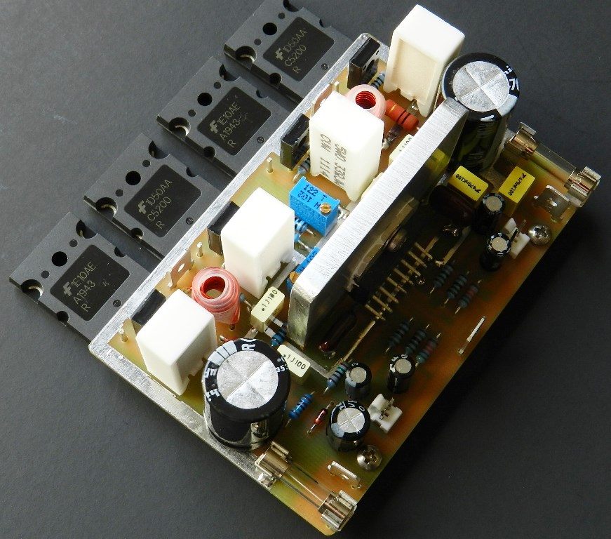
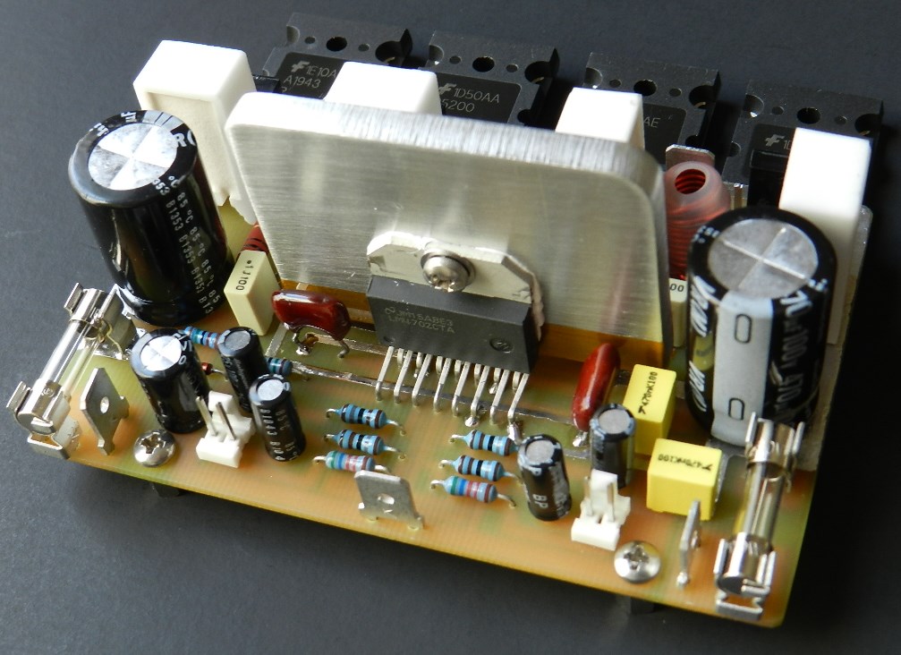
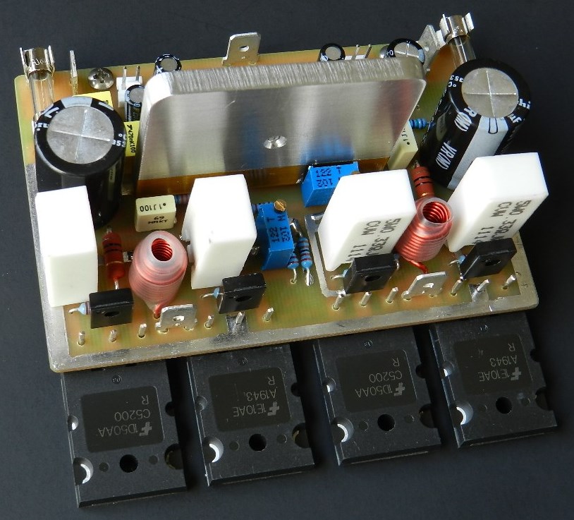
The LM4702 device is limited to 5mA of output drive current capability. TI’s design utilizes complementary Darlington power output transistors, MN2488 and MP1620; to achieve the current gain required to drive an 8Ω load. These components are not easy to find. For this project’s prototype they were replaced with readily available complementary discrete TO126 packaged driver transistors, Q3 thru Q6 and TO264-packaged power output transistors, Q7 thru Q10 (refer to the schematic diagram and BOM). Both genuine devices are available from Fairchild Semiconductor.
According to TI, a new fabrication process was used to create the LM4702 high voltage driver. This allows reduced bias levels while maintaining very low THD+N performance. An external VBE multiplier circuit consisting of Q1/Q2, VR1/VR2 and other associated components set the output stage bias. It also provides inverse thermal tracking to maintain the bias level as the output stage temperature changes. Transistors Q1 and Q2 are populated at the bottom of the PCB and physically make contact with the aluminum bracket as well as the heatsink of the power output transistors. The amplifier achieves very low distortion and noise levels with only about 15 to 20mA of bias current. The ability to set lower bias levels on the LM4702 means less wasted power and less heat.
This project is configured as a non-inverting amplifier with the gain of each channel set by resistors R9/R3 and R10/R6 at 29.1V/V or 29.3dB. The measured power output of this project prior to clipping is about 35 watts per channel at 8Ω with ±45VDC power supply rails. By using the “B version” of this chip, higher power supply rails could be used which could easily realize a power output of about 100 watts per channel or more.
After performing the required initial tests comes what’s considered to be the best part of building this project, the listening test. The prototype unit was connected to a modified LM49720 tone control preamp. While playing “Pepė Linque” by Oregon from their “Beyond Words” album on a Toshiba HD-A2 player and JBL Loft40 speakers, you hear impressive clarity and dynamics, especially the bassist’s musical instrument. Listen to “The Waters of March” by Susannah McCorkle from the Concord Jazz SACD album for vocals and percussion details. The entirety of Zero7’s “Record” album was also auditioned with the same setup for endurance music testing. The prototype was also tested with Project 9, the LM1036 tone control project and a pair of B652 speakers with acceptable results.
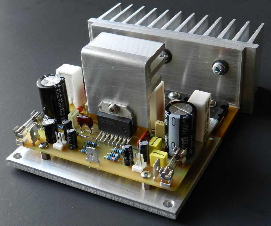
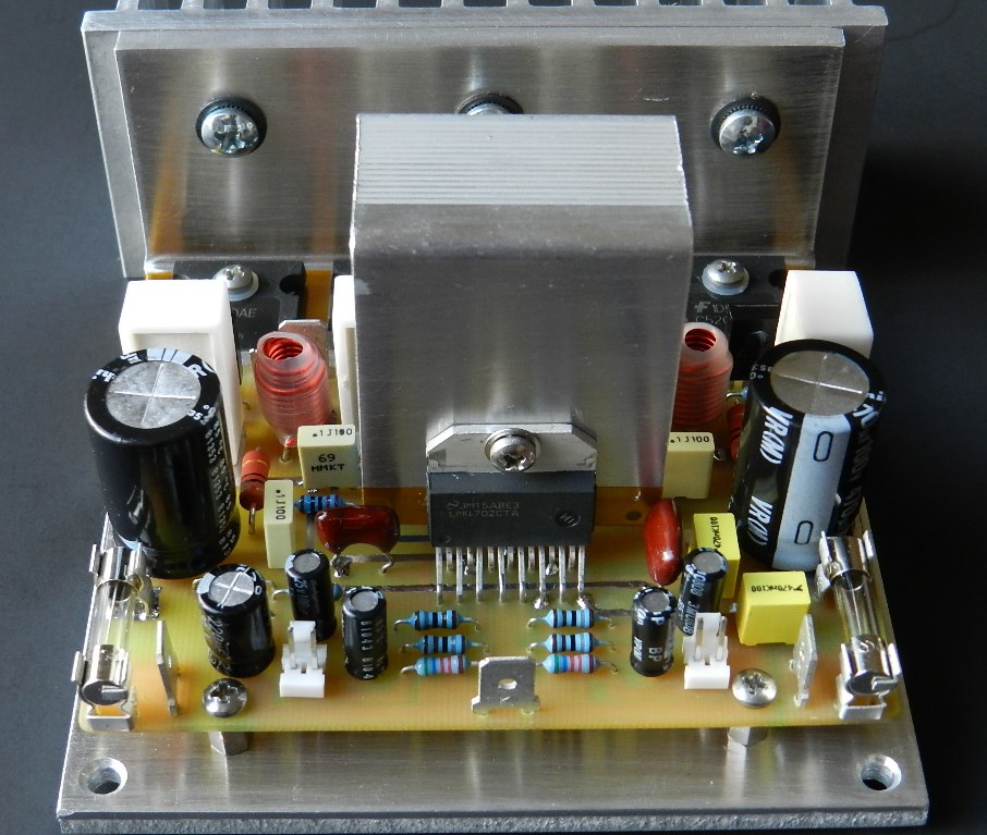
The prototype model was built on a challenging double sided 3.8” X 2.5” PCB. All of the passive components used in the prototype model are standard, commercially available parts. If you are interested in building this project and have read the Information and Policies section of this website, the schematic diagram, actual-sized PCB layout (available only by request) and BOM are free, as is, no warranty.
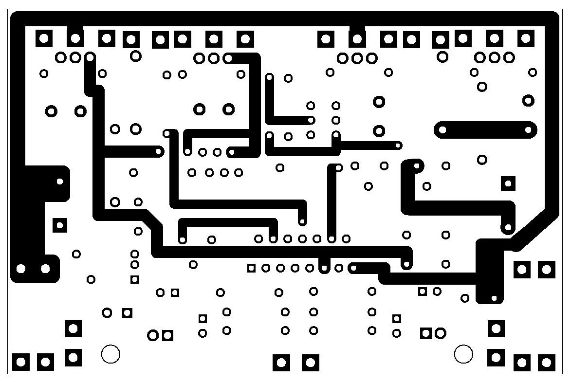
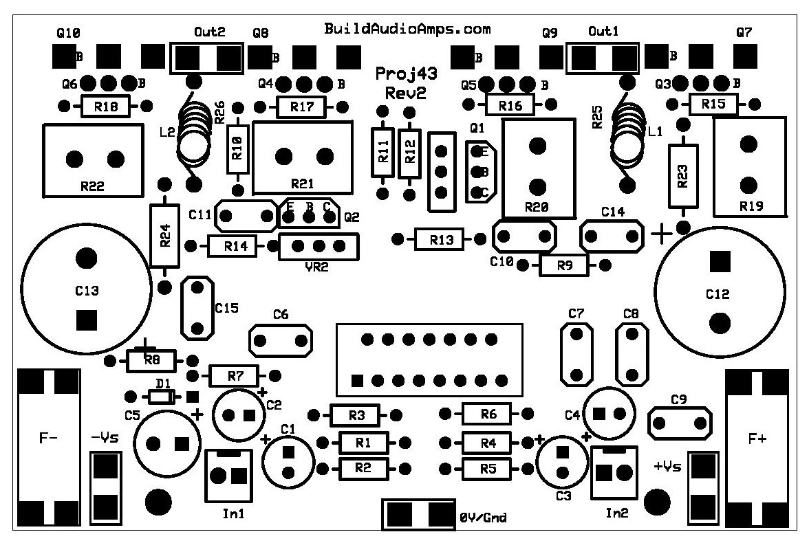
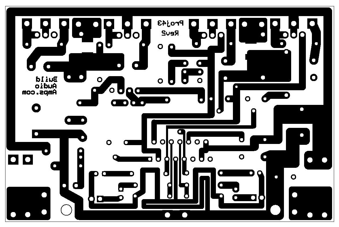 Top Layer Silkscreen Layer Bottom Layer
If you’ve decided to build this project, the idle current needs to be adjusted first before going any further. Insert a jumper or shunt at J1 and J2 inputs of the amplifier. Do not connect any load or loudspeaker at the outputs of the amplifier. Adjust VR1 and VR2 for maximum resistance of 1KΩ; please refer to the schematic diagram where to access VR1 and VR2 on top of the PCB. Prepare 5 DMMs to measure the DC offset voltages at the outputs of the amplifier, the voltage between the emitters of Q7/Q9, Q8/Q10 and the overall current across the F+ fuse terminals.
Why all the DMMs? The very first time you apply power to a newly built audio amplifier project the DMM is your very best friend. The DMM tells you instantly if there is something wrong with your printed circuit board assembly. A very high ammeter reading indicates that a component in the circuit is drawing too much current. The same goes with a very high voltage reading at the output of the amplifier where you should expect a very low voltage reading in the millivolts range. The DMM tells you the bad news first and when the inevitable happens you immediately switch OFF the power supply and recheck the assembly. If you don't have all the DMMs connected to those important test point locations mentioned and when that tragic event happens, you only have your senses to tell you something is burning or smoke signals are coming off from the populated components. The DMM likewise tells you also the good news when everything works just fine and that you did a good job!
It is highly recommended to use a Variac transformer when performing the initial test of the project. If something goes wrong with the project, minimum damage will occur to the components or just a blown Variac’s fuse. However both test procedures with or without the use of a Variac transformer will be explained.
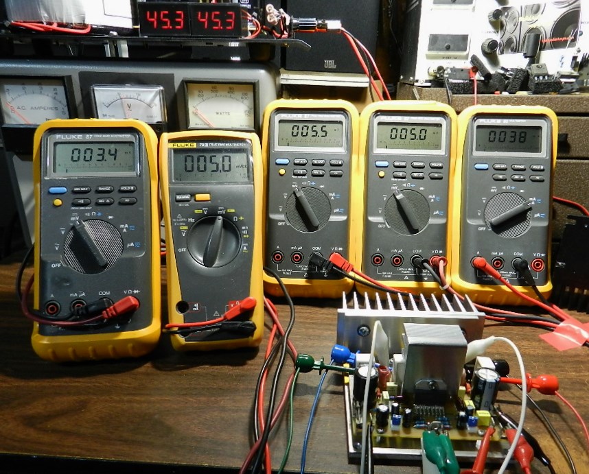
If a Variac transformer is available, connect the AC input of the power supply to the output of the Variac transformer. Switch the power to ON and gradually adjust the Variac’s AC output from zero until the voltage output of the power supply reaches approximately ±45VDC while observing for sudden increase in any DMM readings. If you have encountered an unusual increase in any of the DMM readings, switch the power to OFF immediately and check the PCB for assembly errors. The picture above shows a DC offset voltage for channel 1 at 3.4mV and 5.5mV for channel 2. The voltage between the emitters of Q7/Q9 is 5mV as well as the emitters of Q8/Q10; readjust VR1 and VR2 to get approximately that DMM reading after a warm-up period of 10 minutes or more. From the prototype test results, it was determine that this bias voltage is the minimum actual value that produces a well-rounded peak on the output waveform. The current across the F+ fuse terminals is about 38mA; this value is dependent on the adjustment of VR1 and VR2. If you obtain similar DMM readings, you may proceed with music test.
If a Variac transformer is unavailable, make sure that the power supply was properly built and that the output voltage rails have been measured approximately ±45VDC before connecting it to the amplifier project under test. With the power supply switched to OFF, adjust VR1 and VR2 for maximum resistance. Switch the power supply to ON; the DMMs measuring the voltage between the emitters of Q7/Q9 and Q8/Q10, should read less than 1mV. The DMMs measuring the offset voltages should read about 3mV to 6mV. The DMM across the fuse terminals should read less than 30mA. Other than DMM readings mentioned, power OFF immediately and check the PCB for assembly errors. When the error was corrected, adjust VR1 and VR2 to get a DMM reading of 5mV for each channel after a warm-up period of 10 minutes or more. The DMM that’s connected across the F+ fuse terminals will read about 38mA of total current. If you obtain similar DMM readings, you may proceed with music test.
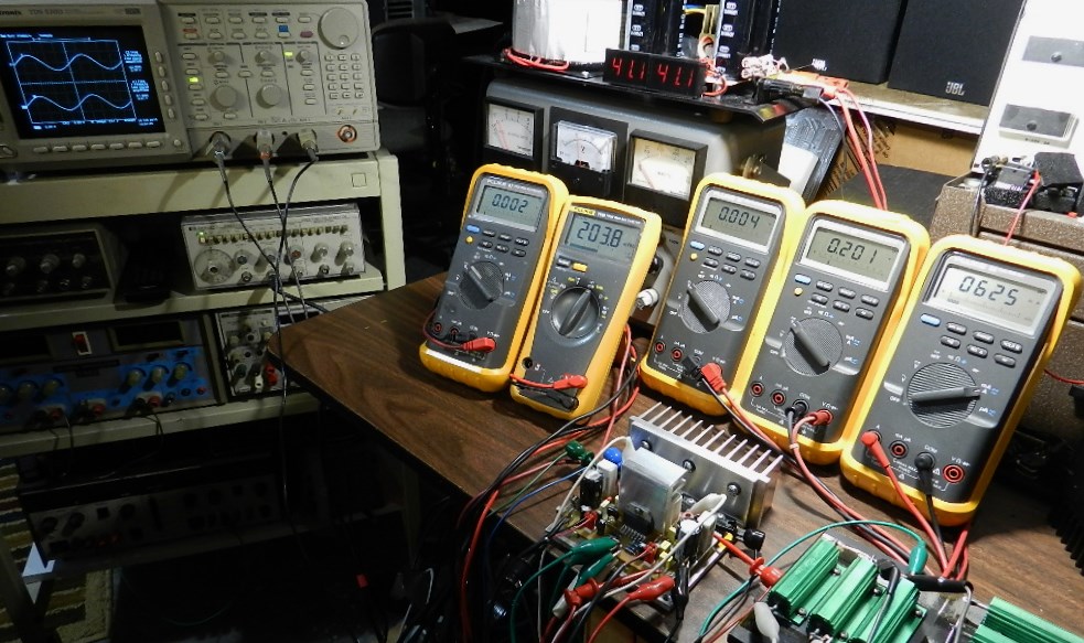
The next test procedure is optional, but if an oscilloscope, audio signal generator and 8Ω dummy loads are available, the maximum power output before clipping can be measured. Be careful not to touch the project’s heatsink and dummy load, it will get very hot during this test.
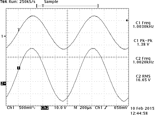

Single channel power measurement at 35 watts. Output waveform for both channels at 19 watts/ch.
The power output was measured using an HP3312A Function Generator set at 1KHz 1.38Vp-p sine wave output and connected directly to the inputs, J1 and J2, as well as the CH1 test probe of the oscilloscope. An 8Ω/100Watt dummy load was connected at the output of the amplifier of each channel under test as well as the CH2 and Aux1 test probes of the Tektronix TDS520D 500MHz DPO. The project’s prototype produces 16.65Vrms across the 8Ω/100W dummy loads, which is equivalent to a power output of approximately 35 watts per channel, as shown in the TEK hardcopy pictures above. The oscilloscope’s horizontal scale was adjusted at 200uS to verify for any visible clipping or artefacts on either peak. Enjoy!