
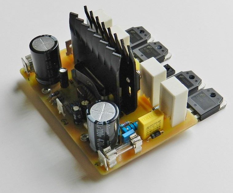
Project 8


Another build your own audio amplifier project uses Texas Instruments' LME49811 a high fidelity audio power amplifier input stage designed for pro-audio applications. Increasing the power supply voltage and the number of output devices may scale the amplifier's power output. The LME49811 is capable of driving an output stage to deliver in excess of 500 watts single-ended into an 8-ohm load in the presence of 10% high line headroom and 20% supply regulation.
The LME49811 includes a thermal shutdown circuitry that activates when the die temperature exceeds 150° C. The LME49811's shutdown function when activated, forces the LME49811 into shutdown state.
• Wide Operating Voltage Range: ±20V to ±100V
• PSRR (f = DC): 115dB (Typ)
• THD+N (f = 1kHz): 0.00035% (Typ)
• Output Drive Current: 9mA
The first LME49811 amplifier prototype model that I built uses the typical application circuit presented in the application notes SNAS394C. The audio quality it reproduced was in my opinion very impressive. For that reason, I have built more than 20 or so different power output stage topologies that uses an LME49811 as the input stage. The PCB layouts and schematics have been developed and several of them will be featured as future projects in this website. The pictures are shown in the Tinkerer's Workshop.
The schematic diagram have been redrawn to show some modifications to the typical application circuit . The Part IDs in the schematic diagram corresponds with the silkscreened Part IDs in the PCB. If you want to build Project 8, a PCB layout as well as the Project8 BOM are provided for free, as is, no warranty. The fun part of this project is populating the LME49811’s 15 pins arranged in 2 rows into thePCB. Patience is a virtue!
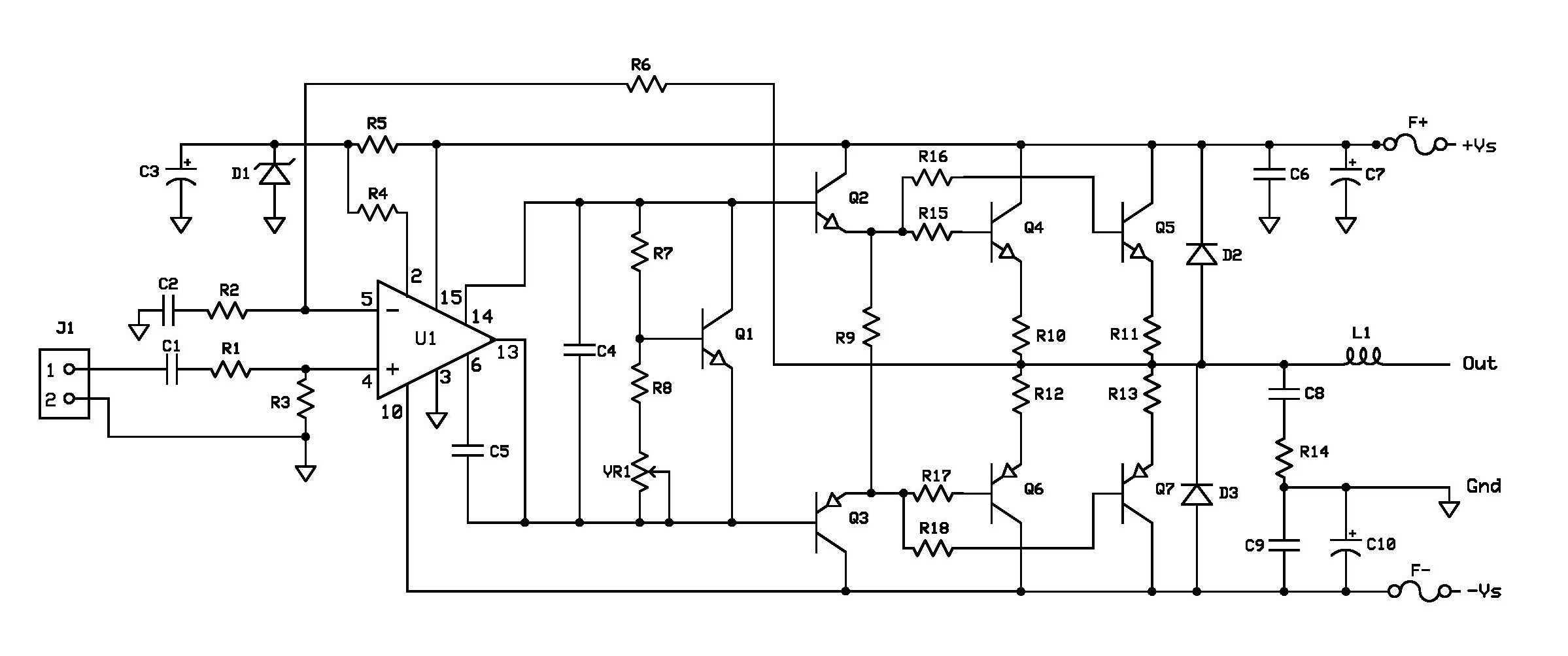
Project8 Schematic Diagram
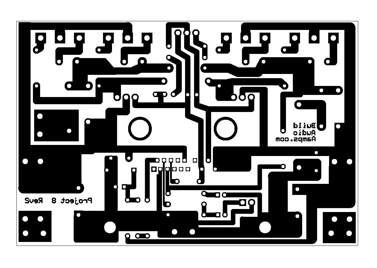
Project8 Bottom Copper Layer
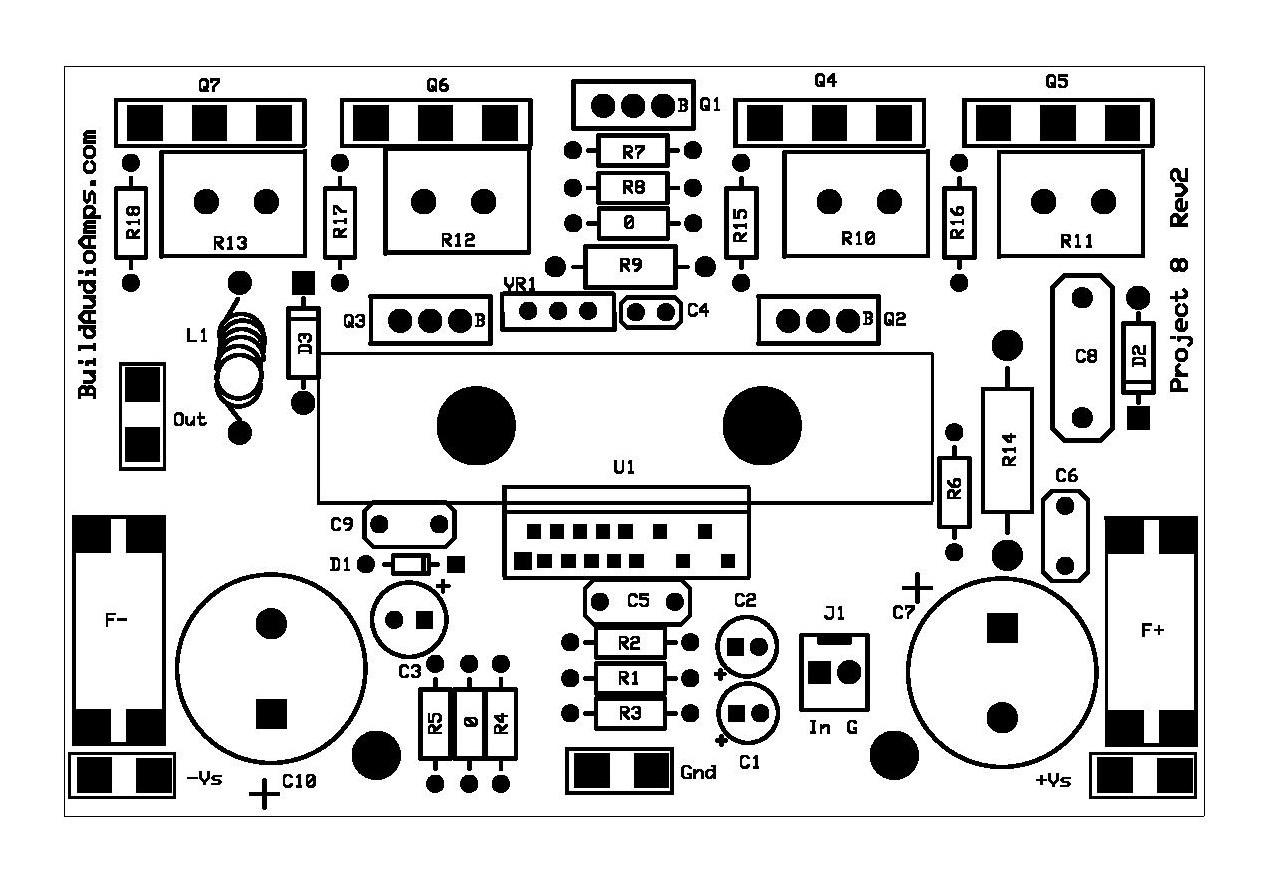
Project8 Silkscreen Parts Placement Layer
Project 8 is a non-inverting configuration and the gain is determined by the ratio of R6 (Rf) and R2 (Ri). TI recommends that the gain should be set no lower than 26dB otherwise LME49811 may experience instability, however for this project the gain is set at about 29.88 or 30dB. TI also recommends between 1mA and 2mA of current should be flowing into the shutdown pin 2, the IC will be in “play” mode meaning it is enabled, without this flow of current the IC will shutdown or “muted”. A 5VDC supply across D1 is connected through a 1.4kΩ resistor to pin 2 will result in shutdown current of 1.5mA, right in the middle of the specified range.
The LME49811 has a built-in thermal protection circuit to prevent long-term thermal stress of the device. When the temperature on the die exceeds 150°C or 302°F (that's really hot) LME49811 will shut down. It starts operating again when the die temperature drops to about 145°C or 293°F, but if the temperature again rises, shutdown will occur again above 150°C. If this faulty condition occurs again then it is warning you of heat-related issues. In some ways this feature improves thermal reliability of the device. The type of heatsink selected provides ease of IC mounting, thermal robustness, and mechanical stability. But any piece of aluminum scrap of identical dimensions may be used.
C4, compensation capacitor should be populated in close proximity to the LME49811 pins and mica type to provide very good audio performance.
Q1 also called a Vbe multiplier together with VR1, adjusts the bias of the output power transistors. Q1 is mounted near the power transistors to track changes in temperature. Proper adjustment of VR1 can also effectively minimize crossover distortion of the amplifier.
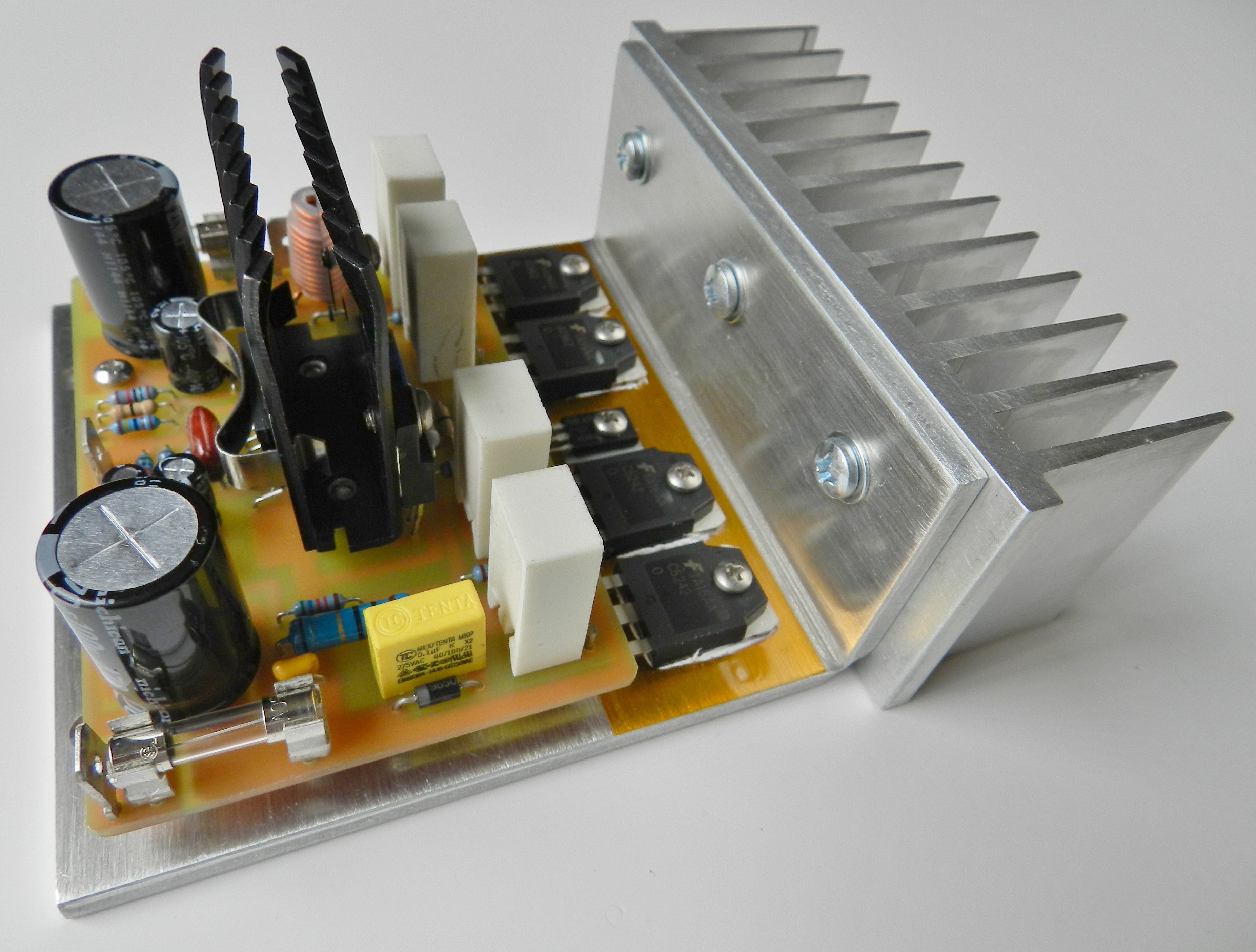
For this project I'm using 2 complementary pairs of 2SC5242/2SA1962 as the power output transistors. The driver transistors can either be 2SC3503/2SA1381 in T0126 packages or 2SC4793/2SA1837 in T0220 packages. R10, 11,12 and 13 are the emitter degeneration resistors. These resistors prevent the power transistors from going into a condition called thermal runaway.
The emitters of the complementary driver transistors Q2 and Q3 are connected together by R9. This configuration offers better performance than Darlington output stage used by TI’s typical application circuit. R15, 16, 17 and 18 are the series base resistors, it improves stability of the parallel-connected power output transistors Q4, 5, 6 and 7. A network of C8, R14 and L1 at the output are used to improve the stability of the amplifier at any loads. Missing in the circuit is a resistor in parallel with L1; this is a 4.7Ω 2Watt SMT-type resistor populated at the bottom copper layer of the PCB.
Although LME49811 has excellent power supply rejection and does not require a regulated supply, C6, C7, C9 and C10 were added to eliminate low and high frequency instabilities.
After completing the PCB assembly, the idle current of the power output transistors must be adjusted. Insert a shorting jumper or shunt at the input, J1. Adjust the multi-turn VR1 counterclockwise to read 0Ω on an ohmmeter*. This can be accessed at the emitter of Q1 and one end of R8, please refer to the schematic diagram. Connect a millivoltmeter* at the output and ground pcb terminals to measure the dc offset voltage. Connect a millammeter* at F+ fuse terminals to measure the idle current. For this test I will be using a ±54VDC power supply. You can use a lower voltage ±24VDC power supply for testing purposes and just to be safe! A ±32VDC to ±54VDC at 3A to 6A power supply is recommended for this project.
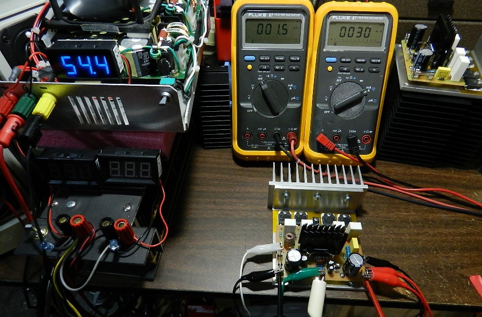
The 2 DMMs should be connected as shown in the picture. The DMM on the left is measuring the DC offset voltage at about 1.5mV and the DMM on the right is measuring the idle current at about 30mA. Adjust VR1 clockwise to get this value and needs to be readjusted, if necessary, after 15 minutes or so. If your tests results were different, switch OFF the power supply immediately and check the PCB for assembly errors. If you got it right, proceed with music test!
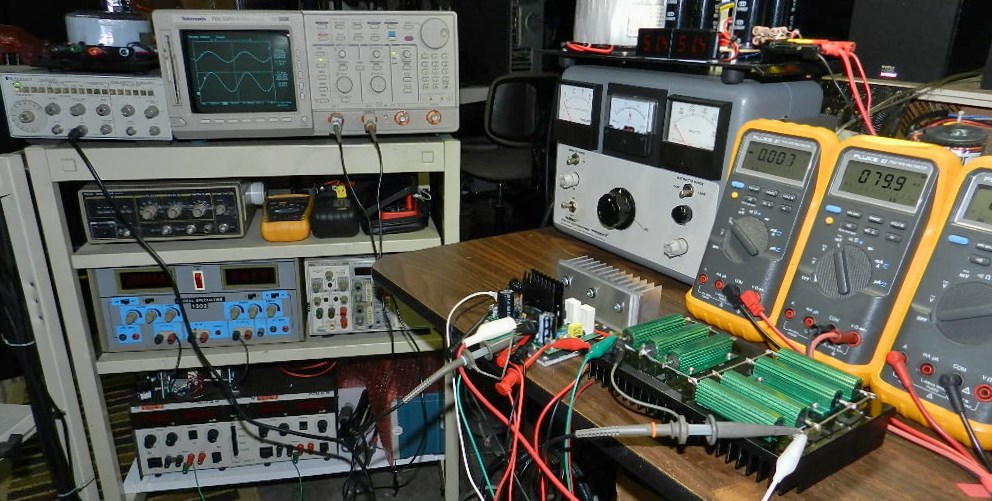
If an oscilloscope, audio signal generator and 8Ω dummy load are available, the power output of this amplifier project can be measured. If not, the following pictures will show you that!

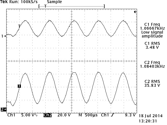
A 1KHz 3.48Vrms sine wave signal is applied to the input of the amplifier under test, produces a 35.83Vrms across an 8Ω/400W load, or a power output of about 160Wrms at 8Ω just before clipping occurs.

Project 8 installed on a 3/16" thick aluminum mounting bracket.
*this refers to one of the basic functions of a DMM.
Updated 10/11/2014 test result for Project 8:
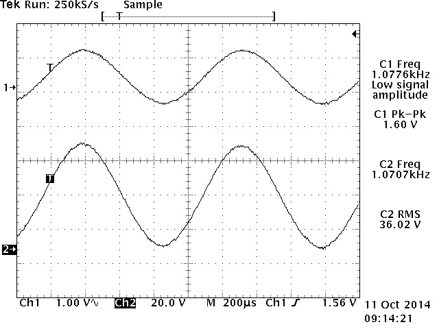
The previous power output measurement test result for this project uses ±54VDC supply rails from SMPS modules. The updated test uses a conventional unregulated ±54VDC to ±65VDC power supply rails. Notice the Tek hardcopy picture above shows an improvement to the input as well as the output waveforms. Both waveforms do not show any signs of RFI or EMI noise artifacts inherent to most Switch Mode Power Supply designs. A switch mode power supply (SMPS) is very good at maintaining its specified voltage and current output and is very efficient in doing just that but its output rails contains electrical noise, as evidenced in the previous test result. It’s amazing how the LME49811 tried to put up a good fight with a dirty power supply and won! The SMPS modules that I’ve used were quite difficult to clean up the noise in the output rails because it does not startup normally if capacitive loading were increased.
The function generator was set for a sine wave output and adjusted at 1KHz 1.6Vpp output signal and connected directly to the input of the amplifier under test as well as the CH2 test probe of the oscilloscope. An 8Ω/700W dummy load was connected at the output of the amplifier under test as well as CH2 probe of the oscilloscope. The power amplifier produces 36.02Vrms across the 8Ω dummy load or a power output of 162Wrms.
If you’re interested in putting up together a power supply for this project, here’s AN-1849 application report by Texas Instruments. This application report provides design information for a power supply for use with the LME series of audio amplifier input stage ICs, but it can also be used for other projects presented on this website.
![]()