Project 45


Introduction. Project 45 features a fully symmetrical current feedback audio power amplifier. CFA-based audio amplifiers have extraordinary sonic qualities that can only be experienced and appreciated when you build one for yourself. In a voltage feedback amplifier (VFA), the differential input stage produces a voltage difference in its output when the input and feedback signals are applied to its inputs simultaneously. While in a current feedback amplifier (CFA), the input buffer and summing amplifier stages produce an error current output when the input and feedback signals are applied to its inputs simultaneously. As their topology names would imply, it is either a voltage or current output that is produced by the front-end stages of the audio power amplifier. The most distinguishable component that differentiates both topologies is the value of the negative feedback resistors. With reference to several schematics, the negative feedback resistors of CFAs are 10 to 20 times lower than most VFAs. There’s no feedback capacitor in series with a resistor to signal ground in current feedback amplifiers.
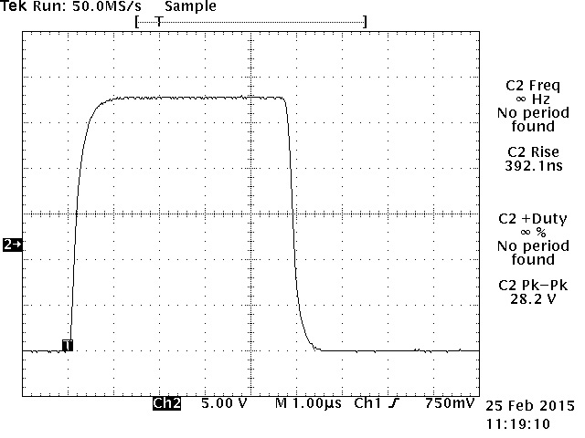
General comparison between VFA and CFA topologies. VFAs have slower slew rate. Slew rate is how fast the output of an audio amplifier can change with respect to the input signal, expressed in volts per microseconds (V/uS). CFAs are mostly capable of faster slew rate, as actually measured in the prototype with a 100KHz square wave rise time at 392.1nS. However, CFA-based amplifiers have disadvantages too, which include somewhat poor DC offsets that have thermally induced settling time, as encountered in this project. There’s also a downside in its stability with regards to the choice of feedback resistors and compensation capacitors.
There’s limited web information that can be found regarding CFA-based audio power amplifiers except that they are widely used in operational amplifier integrated circuit applications, like this article from Intersil. The top search results listed Analog Devices Application Note AN-211 entitled “The Alexander Current-Feedback Audio Power Amplifier” by Mark Alexander. Here the author describes his design of an audio power amplifier project utilizing an op-amp as the current feedback component at the input stage, a second op amp integrator for DC offset control and power IGBTs at the output stage. The project’s author concludes that CFAs can offer superior sonic performance to all known topologies during the time his project was built.
A similar but simpler audio power amplifier project is also well described at www.andiha.no. This is a DIY website with interesting articles all about audio in general. You can find the topic under the Current Feedback Amplifier menu. This website explains the basic principle of current feedback by providing the readers with a CFA-based 25 watts per channel Class A power amplifier project. The schematic looks achievable to build as a future CFA project and uses a smart way of utilizing JFETs at the input stage configured as a buffer and error amplifier at the same time.
The CFA-based topology is also commercially available by audio power amplifier manufacturers like NAD, Accuphase, Sony, Arcam and etc. These manufacturers describe their products as having superb sonic qualities with excellent frequency response characteristics. There’s also another CFA advocate at hifisonix.com.
It’s now time to build a prototype of a current-feedback audio power amplifier and listen!
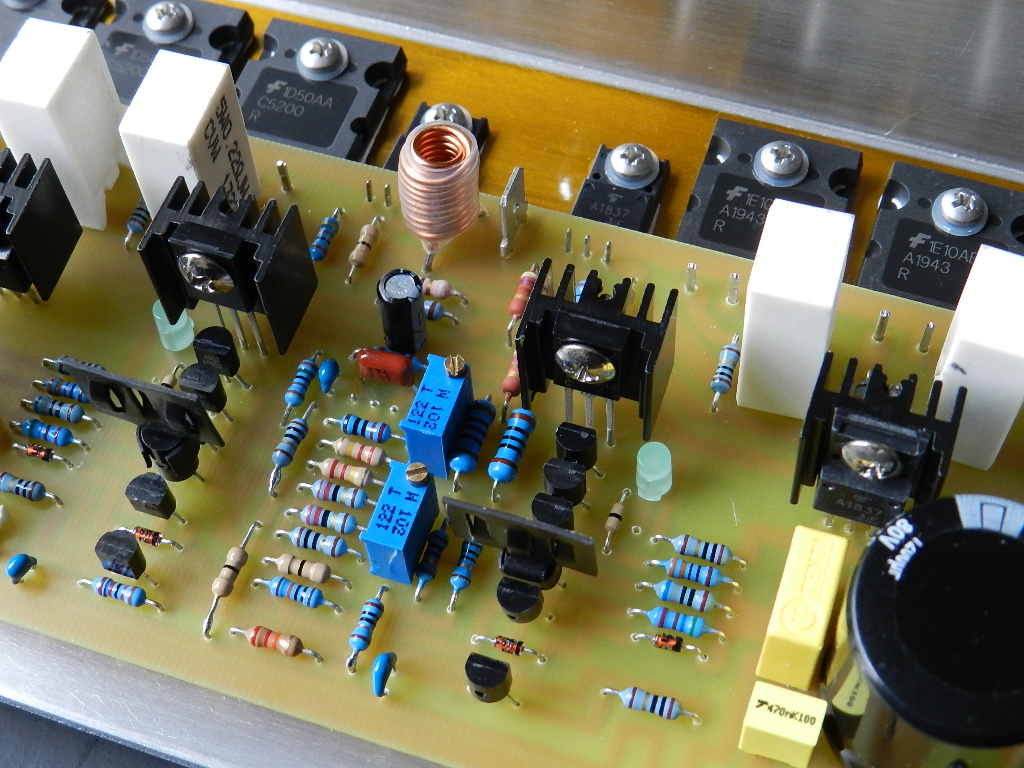
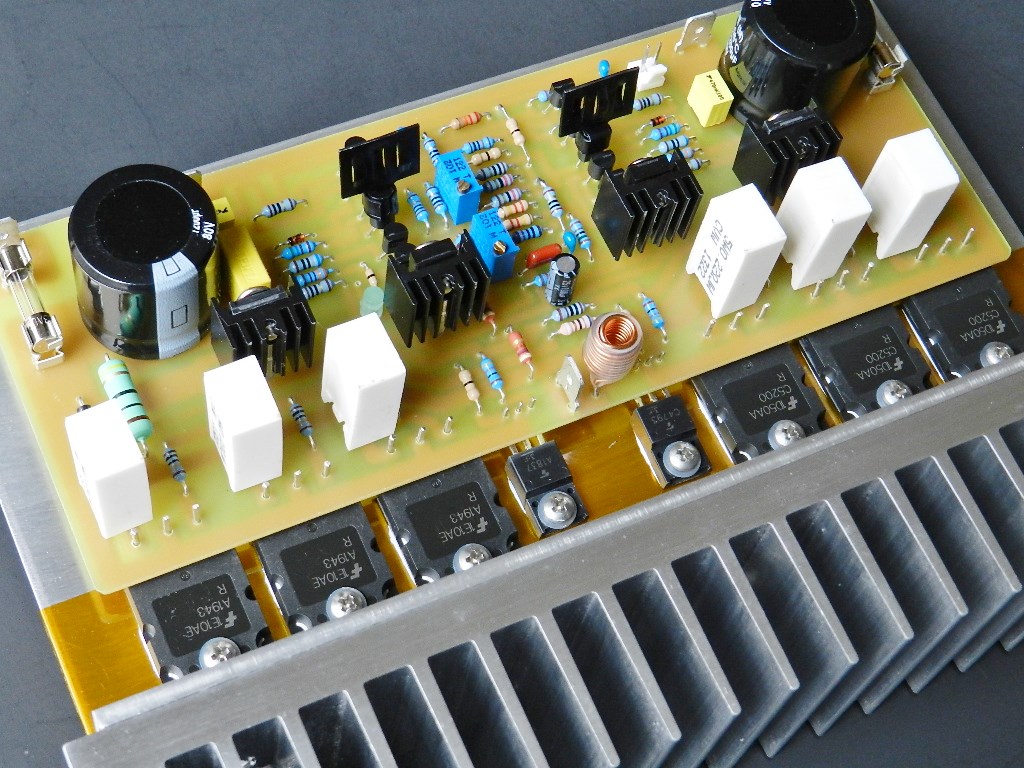
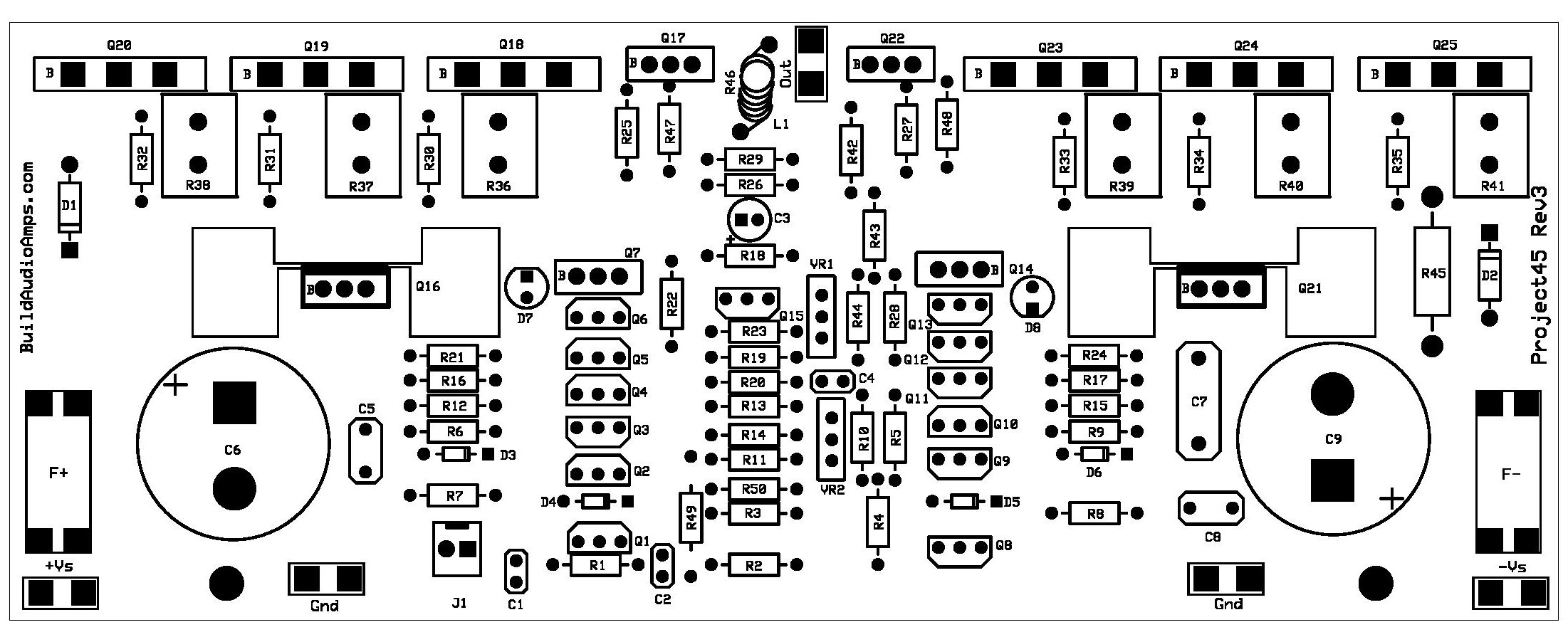 Project 45 Silkscreen Parts Placement Layer of PCB.
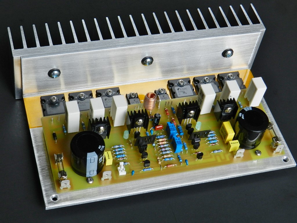
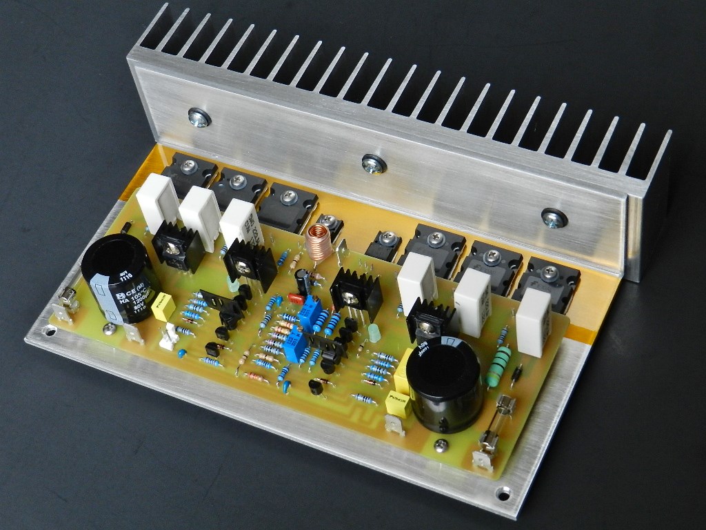
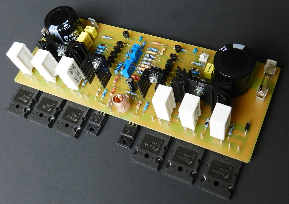
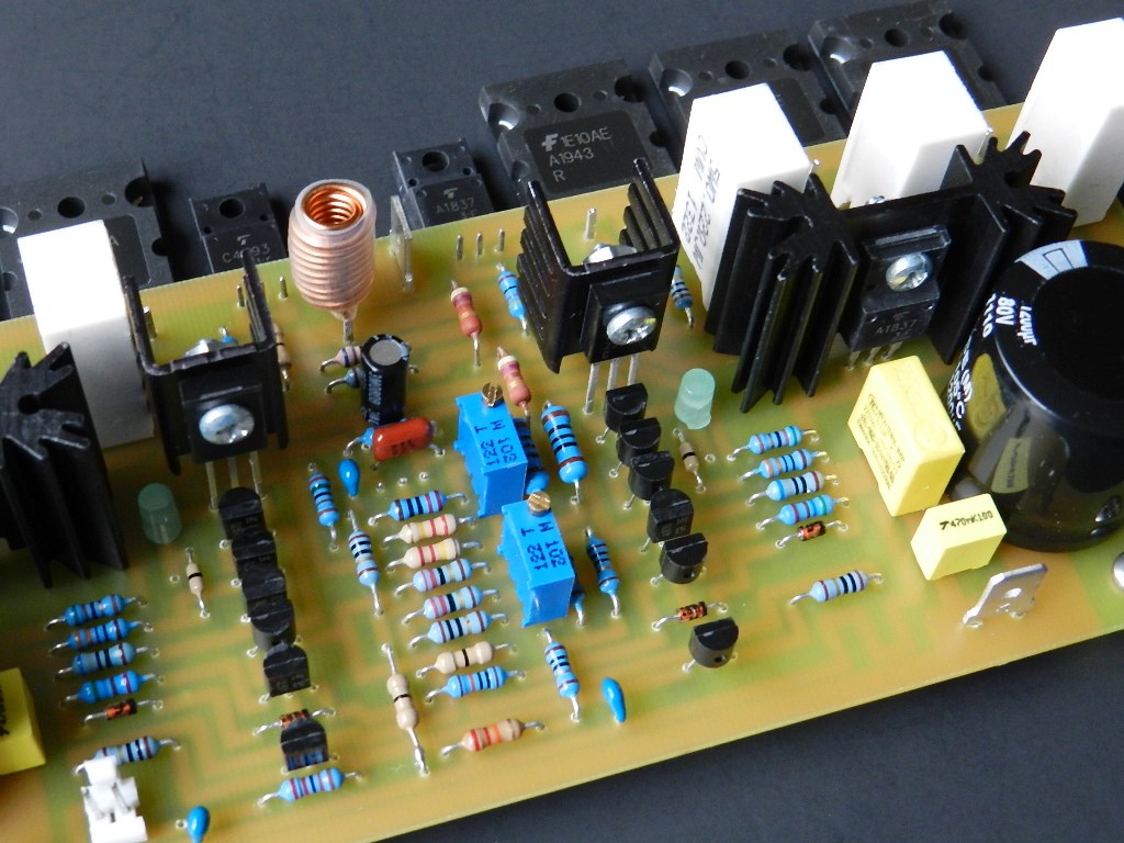
Here’s a brief description of the prototype’s circuit: The input signal from J1 is DC coupled to the bases of the emitter-follower buffer transistors, Q1 and Q8. Q2/D3/D4 and Q9/D5/D6 provide about 1.1 mA of current for Q1 and Q8 respectively. The feedback current from the main output of the amplifier by way of R42, R43, R44 and R28 is connected to a node point at the emitter resistors of the summing error amplifier transistors, Q3 and Q10. Since the impedance of the node point is low, this feedback is a current. Transistors Q3 and Q10 produce an error current that is dependent to the input signal. These transistors are also sensitive to thermally induced DC offset settling time, also mentioned in the Alexander amplifier. This condition can be compensated with an Aavid Thermalloy P/N 575200B00000G clip transistor heatsink, as installed and shown in the picture of the completed prototype. However, the audio quality is not at all affected by this nuisance. It still sounds great!
Resistors R4, R5, R10 and R11 are also connected at the same node point to signal ground. The value of the feedback resistors determines the overall gain of the amplifier about 29dB. A multi-turn trimpot, VR2, connected in parallel with R13 and R14 also at the same node point, conveniently trims the DC offset voltage by ±200mV. If enhanced DC offset control is desired, an integrator circuit similar to Project 4 could be used to automatically stabilize the DC offset voltage of the amplifier (that’s another future project!). The collectors of Q3 and Q10 are loaded with current mirrors Q4/Q5 and Q11/Q12 respectively. C4 is a high frequency compensating capacitor added to improve the overall stability of the amplifier and its value is also one of the determining factors of the slew rate of the amplifier. The resulting converted current to voltage signal is taken from push-pull cascode transistors Q6/Q7 for the positive and Q13/Q14 for the negative signals. The bases of Q7 and Q14 are constantly biased at about 5.7 mA by D8 and D9. The overall buffered output voltage is available at R19 and R20 with respect to signal ground.
A VBE circuit consisting of Q15, VR1 and other associated components provides an adjustable bias for the output stage transistors. The output stage is a triple emitter-follower configuration capable of producing enough current to drive 4Ω loads. VR1 is adjusted to obtain 22mV across any of the emitter resistors, R36 through R41, which corresponds to approximately 100mA for each power transistor pair. Q18 through Q25 are TO264 packaged complementary pairs of genuine 2SC5200/2SA1943 from Fairchild Semiconductor. Pre-driver transistors, Q16 and Q21, isolate the output of the TIS from the main driver stage and are biased at about 2mA while the main driver transistors, Q17 and Q22, at approximately 13mA. Both stages operate in Class A mode. The measured power output of this project before clipping is more than 130 watts at 8Ω or more than 260 watts at 4Ω with power supply rails of ±54VDC.
The prototype model was built on a 7.25” X 2.8” single sided PCB. All passive and active components used in the prototype model are standard, commercially available parts. If you are interested in building this project and have read the Information and Policies section of this website, the schematic diagram, PCB layout (available only by request) and BOM are free, as is, no warranty.
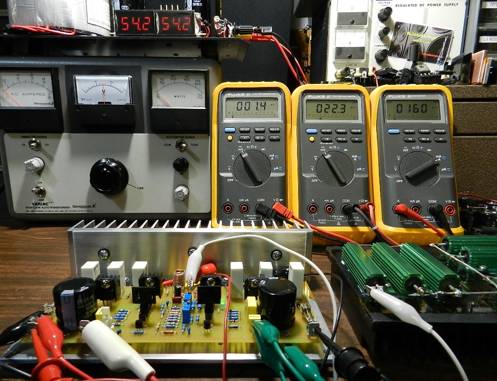
Initial tests. If you’ve then decided to build this project, the idle current needs to be adjusted first before going any further. Insert a jumper or shunt at the input of the amplifier. Do not connect any load or loudspeaker at the output of the amplifier. Adjust VR1 for maximum resistance of 1KΩ; please refer to the schematic diagram where to access VR1 on top of PCB. Leave VR2’s adjustment as is at this time. Prepare 3 DMMs to measure the DC offset voltage at the output of the amplifier, the voltage between the emitters of Q20 and Q25, and the overall current across the F+ fuse terminals.
It is highly recommended to use a Variac transformer when performing the initial test of the project. If something goes wrong with the project, minimum damage will occur to the populated components or at least just a blown Variac’s fuse. However both test procedures with or without the use of a Variac transformer will be explained.
If a Variac transformer is available, connect the AC input of the power supply to the output of the Variac transformer. Switch the power to ON and gradually adjust the Variac’s AC output from zero until the voltage output of the power supply reaches approximately ±54VDC while observing for sudden increase in any DMM readings. If you have encountered an unusual increase in any of the DMM readings, switch the power to OFF immediately and check the PCB for assembly errors. The picture above shows a DC offset voltage at 1.4mV and could be anywhere within ±20mV. Adjust VR2 slowly at this time to get as close as possible to 0mV DMM reading. It may need to be readjusted after 10 minutes or more. The voltage between the emitters of Q20 and Q25 is about 22.3mV; readjust VR1 to get approximately to that DMM reading after a warm-up period of about 10 minutes or more. From the prototype test results, it was determined that this bias voltage is the minimum actual value that produces a well-rounded peak on the output waveform. The current across the F+ fuse terminals is about 160mA; this value is dependent on the adjustment of VR1. If you obtain similar DMM readings, you may proceed with music test.
If a Variac transformer is unavailable, make sure that the power supply was properly built and that the output voltage rails have been measured approximately ±54VDC before connecting it to the amplifier project under test. With the power supply switched to OFF, adjust VR1 for maximum resistance. Leave VR2’s adjustment at this time. Switch the power supply to ON; the DMM measuring the voltage between the emitters of power transistors, Q20 and Q25, should read less than 1mV. The DMM measuring the offset voltage should read anywhere from ±100mV or more. The DMM across the fuse terminals should read about 30mA or less. Other than those DMM readings mentioned, power OFF immediately and check the PCB for assembly errors. After any errors were corrected, adjust VR1 to get a DMM reading of about 22mV after a warm-up period of 10 minutes or more. Adjust VR2 slowly to obtain as close as possible to 0mV DMM reading. The DMM that’s connected across the F+ fuse terminals will read about 160mA. If you obtain similar DMM readings, you may proceed with music test.
Optional tests. The next test procedure is optional, but if an oscilloscope, function generator and 8Ω dummy load are available, the maximum power output before clipping can be measured as well as the slew rate. Be careful not to touch the project’s heatsink and dummy load, it will get very hot during this test.

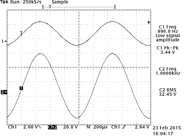
The power output was measured using an HP3312A Function Generator set at 3.44Vp-p sine wave and connected directly to the input of the amplifier, as well as the CH1 test probe of the oscilloscope. An 8Ω/700Watt dummy load was connected at the output of the amplifier under test as well as the CH2 test probe of the Tektronix TDS520D 500MHz DPO. The project’s prototype produces a very nice sine wave of 32.45Vrms across the 8Ω/700W dummy load or a power output of more than 130 watts, as shown in the TEK hardcopy pictures above. The oscilloscope’s horizontal scale was adjusted at 200uS to verify for any visible clipping or artefacts on either peak.

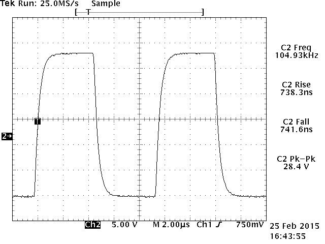
Measured Slew Rate of Project 45. Slew Rate when the value of C4 was reduced. Slew Rate when the value of C4 was increased.
The slew rate was measured using an HP3312A Function Generator set at 100KHz square wave output at 28Vpp. The Zobel network was disconnected during this test, to avoid vaporizing the 10Ω 3watt resistor when a continuous high frequency square wave signal is applied to the input of the amplifier. Do not connect any load at the output of the amplifier under test. The function generator’s output is connected directly to the input of the amplifier, as well as the CH1 test probe of the oscilloscope. The CH2 test probe of the Tektronix TDS520D 500MHz DPO is connected directly to the output of the amplifier. The project’s prototype produces a 103.24KHz square wave rise time of 401.6nS, shown above on the left. This corresponds to a slew rate of 219V/uS. The other two Tek hardcopy pictures show the effect on the slew rate when the value of the frequency compensating capacitor, C4, was changed.
After performing the required initial tests, next is what’s considered to be the best part of building this project, the listening test. The prototype unit was connected to a modified LM49720 tone control preamp. While playing a live recording of “Blue Mind” album by Anne Bisson on a Toshiba HD-A2 player and a Kenwood MV-9D monitor speaker, impressive clarity and dynamics on the entire audio frequency spectrum were experienced. Listening to “Brick House“ performed by Sara K. from her “Hobo” album reproduced the same musical fidelity experience. The entirety of Stanley Clarke Trio’s “Jazz In The Garden” album was also auditioned with the same setup for endurance music testing. There’s more CFA-based projects to come!