Project 53
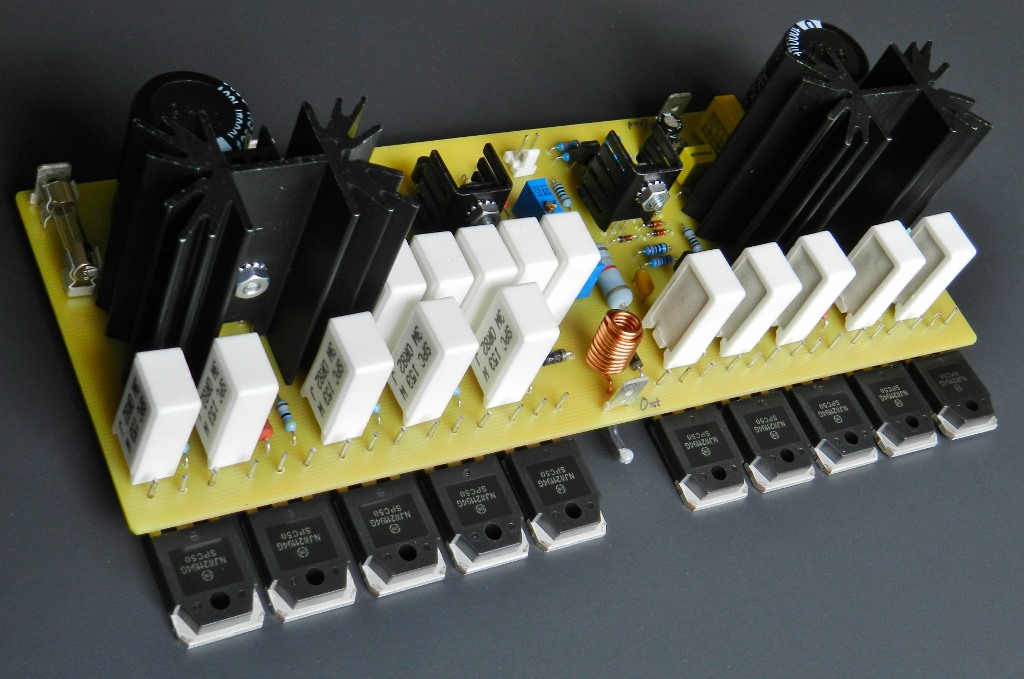
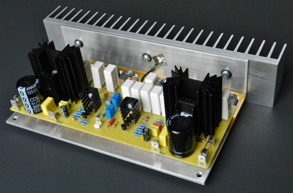
Project 53 is another CFA-based audio amplifier with a quasi-complementary power output stage. Ten NJW21194G are implemented in the output stage to produce high power output when connected particularly to low impedance loads. The prototype model achieved 49.2Vrms across an 8Ω load with ±75VDC power supply rails. This is equivalent to more than 300watts of unclipped audio power output. The actual measurement was acquired by applying a 1KHz sine wave signal with its amplitude adjusted at 6.8Vpp or 2.4Vrms to the input of the amplifier. An oscilloscope measured the output voltage developed across the dummy load. Higher power output is possible by increasing the power supply rails to ±85VDC and additional power output transistors to improve power dissipation.
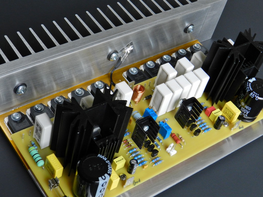
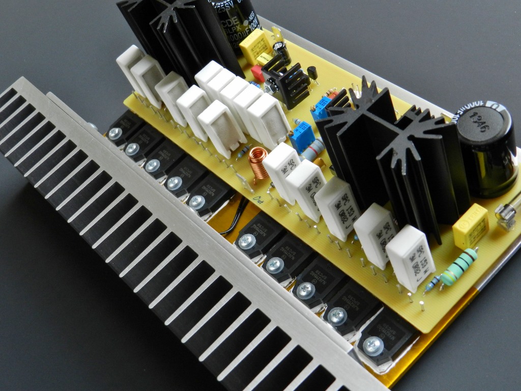
The input stage is similar to previous CFA-based audio power amplifier projects. This was chosen because of its outstanding circuit performance, wider audio frequency response and overall musical fidelity. If you recall in earlier projects, Q9 was used primarily as the temperature-sensing element. However, in this project the VBE circuit was slightly modified to improve the way in which it’s controlling the bias of the power output transistors. To do that, an NTC thermistor was added in parallel with R17 at points A and B locations on the PCB. This is populated off the PCB and mounted anywhere near the heat source, on top of the output power transistors or on the heatsink. As the temperature increases on the heat source, the thermistor decreases its resistance consequently reducing the base voltage of Q9; in effect the bias of the power output stage transistors.
The power output stage drivers consists of Q12 and Q14 in a Darlington pair configuration to amplify the positive half, while Q13 and Q15 in a complementary Darlington pair to amplify the negative half of the incoming signal. A diode was added at the emitter of Q11 (sometimes called a Baxandall diode), which provides improvement in its distortion characteristic, and it gets as good as any complementary symmetrical EF designs. Moreover, the implementation of a CFA-based input stage improved the overall sonic performance of this project. Power output transistors, Q16 through Q25 according to ON Semiconductor, are specifically designed for high power audio output applications. The maximum stress rating for this device is 250 volts, 200 watts, 16 amperes and an operating temperature of up to 150°C.
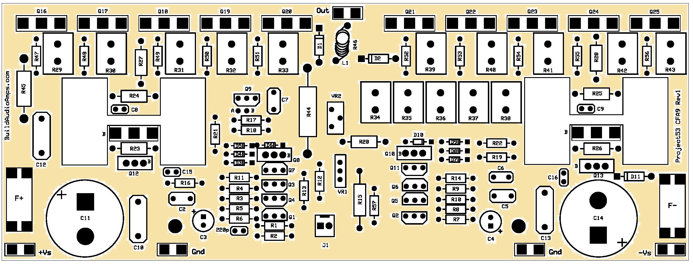
The prototype PCB was created on an 8” X 3” single sided copper board. The schematic diagram, BOM and PCB layout are available only by request.
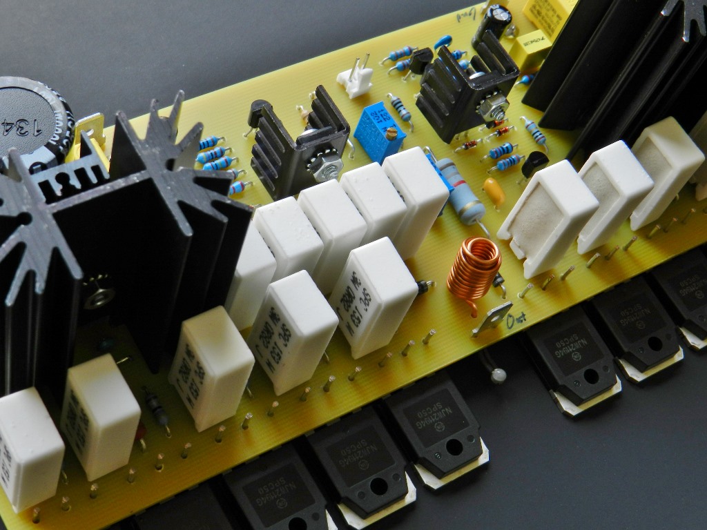
 Project 53 - Silkscreen, Pads and Text on top layer of PCB.
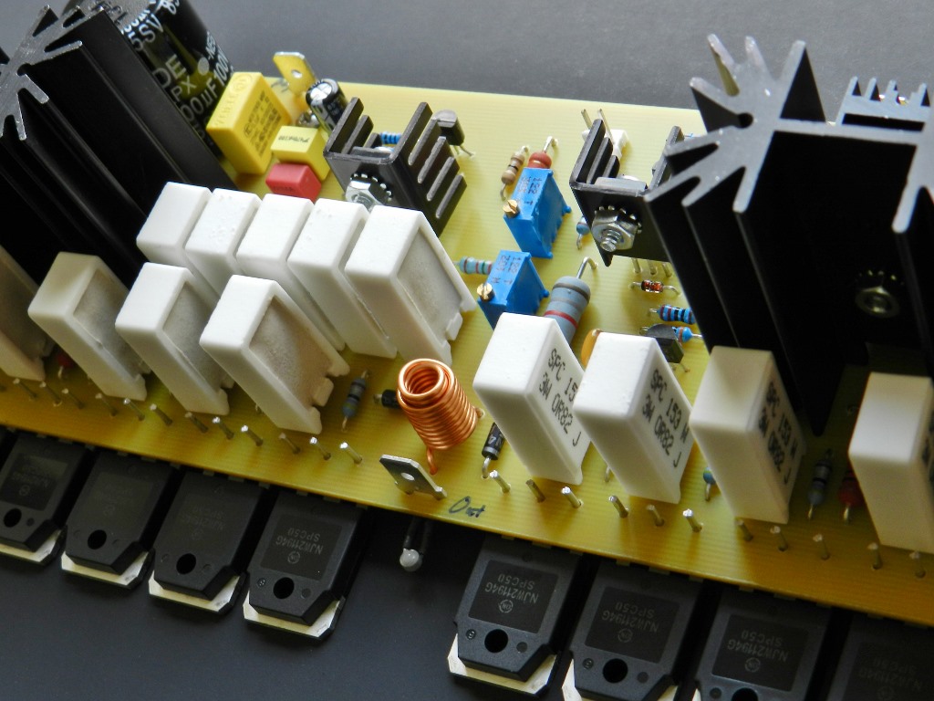
When performing the following tests, always pay attention to what you’ll be doing. You are ultimately responsible for your own safety. You’re applying power to the project the very first time and anything really bad could happen. Furthermore, the succeeding test subjects the components beyond their normal condition and ratings; they may be damaged at any moment without notice. Switch the power to off immediately when you’ve noticed that something went wrong.
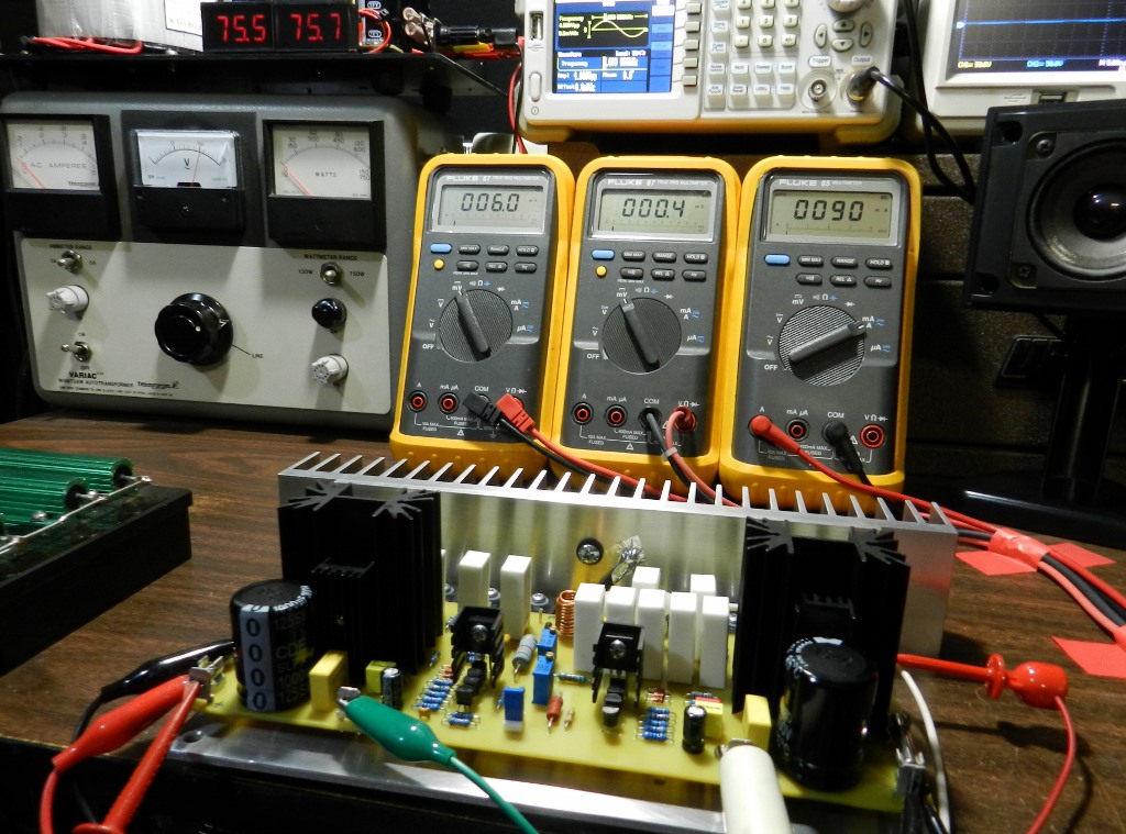
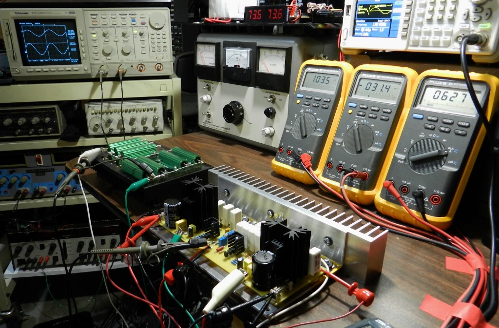
The picture above shows the initial test setup of the prototype. With the power off, adjust VR2 to its maximum resistance at 1KΩ. Do not connect any load at the output of the amplifier. Install a jumper at the input of the amplifier, J1. A variac autotransformer was utilized and recommended, if available, during initial test. As you can see in the above picture, the red LED panel voltmeter reads 75.5 and 75.7. These are the ± power supply voltage rails connected to the project. Allow the prototype to warm-up for about 15 minutes or more before making any adjustments to VR1 or VR2.
The DMM on the left side of the picture is reading 6.0mV; the voltage drop of any emitter resistors, R39 through R43, obtained by adjusting VR2. The DMM in the middle is reading 0.4mV; the DC offset output voltage of the amplifier is obtained by adjusting VR1. This DMM is connected at the output and ground of the amplifier under test. The DMM on the right is connected across the F+ fuse terminals and reads 90mA. This total current reading is dependent on the adjustment of VR2.
If the test measurement results are approximately the same as described, go ahead and perform the best part of building this project, the listening test. If not, you may proceed with the next optional tests.
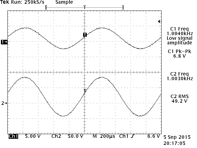
The picture above shows the test setup for power output and square wave frequency response tests. The power output measurement requires an oscilloscope, a signal generator and an 8Ω high-wattage dummy load. A 1KHz sine wave signal (adjusted initially at some low level amplitude) is applied to the input of the amplifier under test. A dummy load and an oscilloscope were connected at the output of the amplifier under test.
Apply power to the project when all the test equipment and cables are interconnected. Gradually adjust the amplitude of the sine wave signal until the output waveform displayed in the oscilloscope reaches just before clipping on either positive or negative peaks. Determine the vertical scale voltage reading in the oscilloscope just before clipping occurs; 49.2Vrms was measured in the prototype, as shown in the Tek hardcopy picture above on the right. Using the formula P = V2 / R, the actual measured power output is 302.58 watts. That’s a lot of watts!
You may also notice that as you gradually increase the signal generator’s amplitude, the power supply voltage rails decreases. This is normal if the VA rating of the power transformer is insufficient. The bench test power supply rails utilized in this test produces more than ±90VDC at 6.2A connected to a Variac transformer. In this case, if the voltage rails were to decrease, adjust the Variac to maintain the required operating voltages for testing purposes.
The power output at 302.58 watts into 8Ω will require about 6.15A of current. Toroidal power transformers like the Avel Y236904 800VA 110CT or AnTek AN-10455 1000VA 110VCT, a GBJL3510 bridge rectifier and 20,000mFd per rail or 10,000mFd X2 per rail is recommended when building a power supply for this project. Here’s a typical example of a power supply design for audio amplifiers by TI Application Report AN-1849.
You might also consider monitoring the temperature of the project while performing this test. The temperature reading of Q12 through Q15 did not reach higher than 60°C. For power transistors, Q16 through Q25, the temperature reading is no higher than 50°C. However, the heatsink temperature reaches more than 80°C after more than an hour test period. It is therefore necessary to use forced air-cooling when performing these tests for longer periods of time.
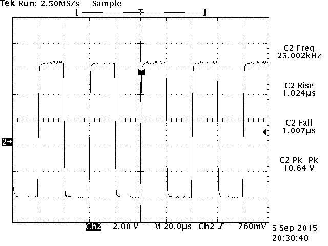
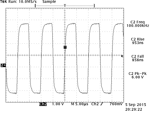
The square wave response or slew rate test requires you to remove R45 off the output of the amplifier under test. Running a continuous high frequency square wave input signal to the amplifier will destroy this resistor. The following pictures will show the 25KHz and 100KHz square wave response output waveforms.
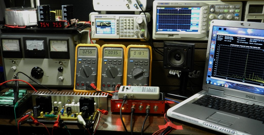
The picture above shows an 8Ω dummy load, Project 53, QA190, QA400, DMMs, Variac/power supply and a Dell laptop computer. This is a simple test setup in performing some basic audio measurements for the power amplifier project with very good results. A QA400 24-bit Real Time Audio Analyzer from QuantAsylum was utilized to measure noise, THD, THD+N, SNR and frequency response. The QA400 is USB powered, controlled by its own application software and can generate and analyze very accurately a series of burst test tones. For this test, the USB hardware was connected to a Dell laptop computer that’s running a Windows 7 operating system.
The input clipping level on the QA400 is +3dBV or 4Vpp. As it is, that’s good enough for testing low voltage level preamplifier or tone control projects. It is however a problem when testing a power amplifier that produces very large amount of voltage. To avoid this damaging condition to the QA400, it is necessary to attenuate the high voltage signal coming from the output of the power amplifier project. One of several ways is to connect a QA190 Low Noise Differential Probe to the input of the QA400. The QA190 clamps the high-voltage signal from the output of the amplifier under test to safe level of about ±4 volts. The QA190 is battery powered and is also fitted with a selectable /10 and /100 range switch for convenience. With the protection of the QA190 in place you don’t have to worry about destroying the QA400.
The left or right channel signal generator output of the QA400 is directly connected to the input of the amplifier under test. Depending on the type of measurement, the signal generator generally generates a 1KHz sine wave signal at -10dB with a sweep from 20Hz start frequency up to 20KHz stop frequency span; however, all these values are user definable. You can also safely monitor this signal by connecting an oscilloscope at the input of the amplifier under test. The next captured QA400 display area pictures will show the test results of Project 53. The prototype’s DC offset voltage and idling current were verified prior to performing these tests.
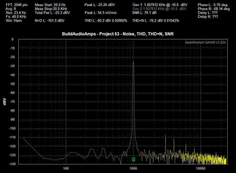 Project 53 QA400 Audio Analyzer - Noise, THD, THD+N and SNR Test Result
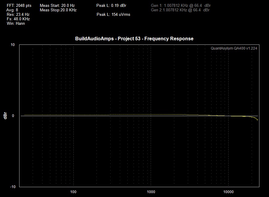 Project 53 QA400 Audio Analyzer - Frequency Response Test Result
How does it sound? “Let Jason Goldenears, an acoustic malcontent, decide”. In real world listening with various music materials, the experience did not disappoint, considering that this is a quasi-complementary based power amplifier. The prototype unit was connected to a passively modified LM49720 tone control preamp, a Toshiba HD-A2 player and several test speakers. Several CD albums were also auditioned during listening test. It’s difficult to distinguish the sonic quality between this project to a full complementary symmetrical power output stage amplifier. However, some listeners might inconclusively perceive a subtle difference only when listening to certain specific music genre. If properly built you should be able to replicate the prototype.
Previously, Phillips launched the professional “Golden Ears Challenge” training program. This is a test of how good your ears are able to detect slight differences in sound quality based on timbre, details, spatial impression, bass and loudness attributes. I took the challenge, completed and was awarded an elite Expert Listener by Philips on 10-Nov-2015.