Project 35
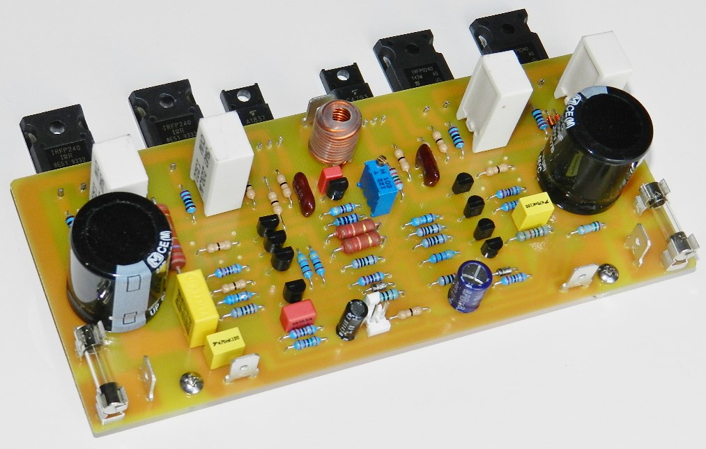
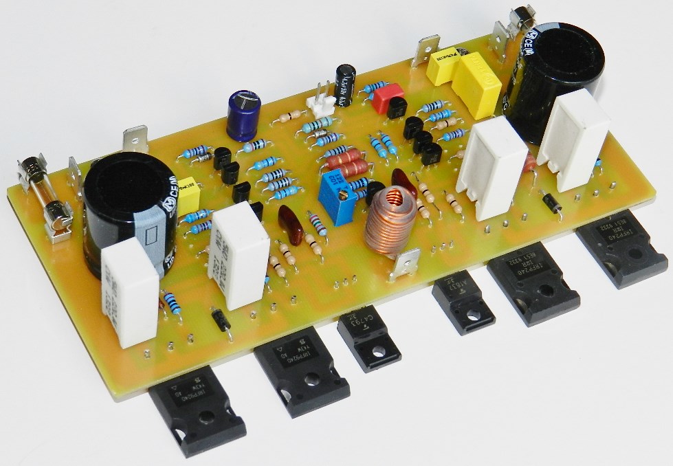
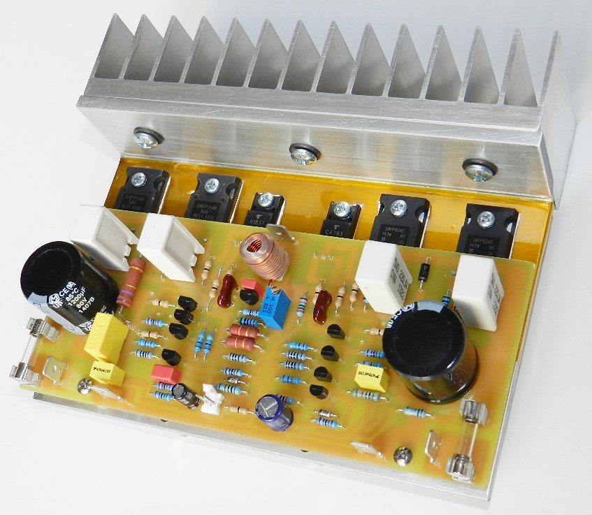
Project 35 utilizes the same circuit from the previous project that uses a symmetrical differential amplifier input stage. Rather than BJTs in the power output stage this time it’s MOSFETs, arranged in a source-follower configuration. In the original design, lateral power MOSFETs were required that regrettably are no longer manufactured by Hitachi. However, Exicon, Semelab and Renesas still manufactures expensive lateral power MOSFETs specifically made for audio power amplifiers. Because of the availability and cost of lateral MOSFETs, an alternative component that is common in most parts bins would be the inexpensive and reliable vertical power MOSFETs. HEXFET is International Rectifier’s signature product line of power MOSFETs and that’s what’s going to be used for this project. IR, Vishay-Siliconix as well as Samsung Electronics manufactures identical power MOSFET part numbers.
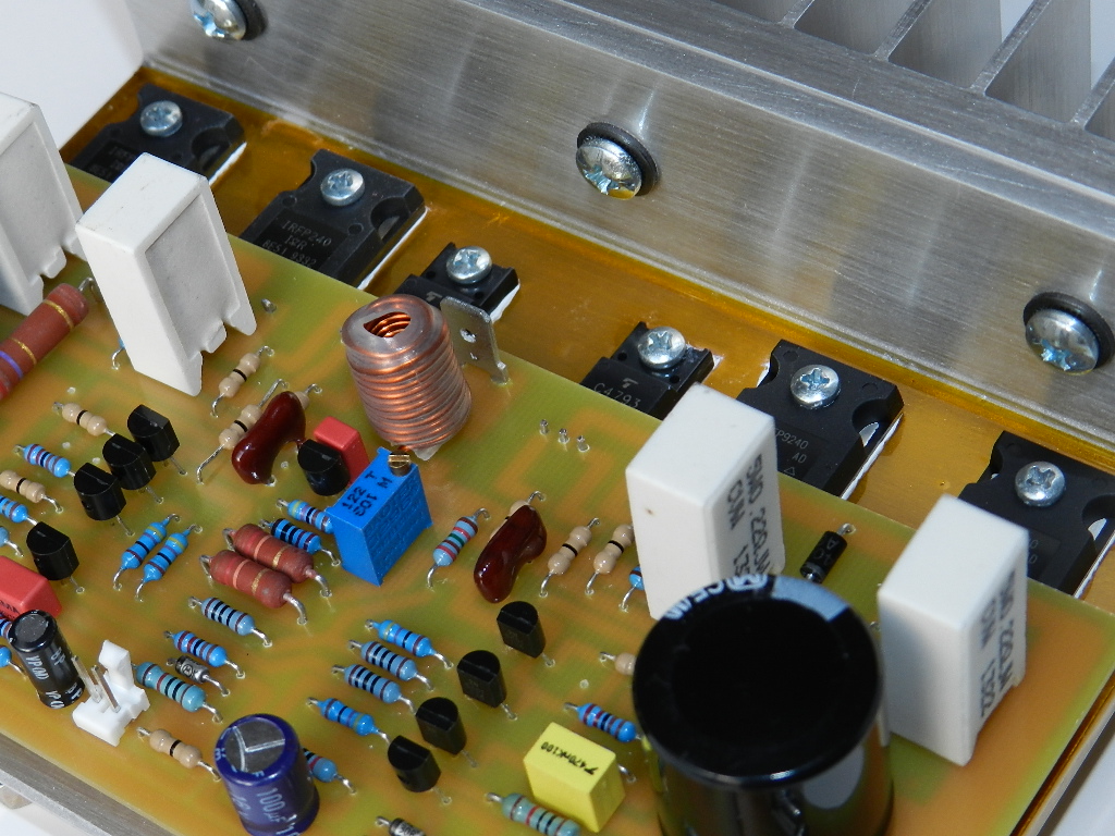
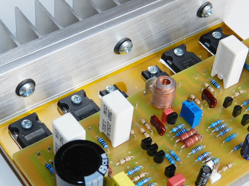
Several modifications were made to the previous circuit so that it could properly work with the vertical power MOSFET output devices. The PCB layout was modified to accommodate some circuit improvements as well as the pin outs for the HEXFET devices. The previous changes that were made to the original design surprisingly work well with the HEXFETs but the value of R34 at the output was reduced while C4 and C5 were replaced with mica capacitors for better audio quality; please refer to the project’s schematic diagram. The prototype model produces more than 100 watts of audio power into an 8Ω load with a ±49VDC to ±55VDC power supply rails and performed superbly during music tests.
If you are interested in building this project and have read the Information and Policies section of this website, the schematic diagram, PCB layout (available only by request) and BOM are free, as is, no warranty.
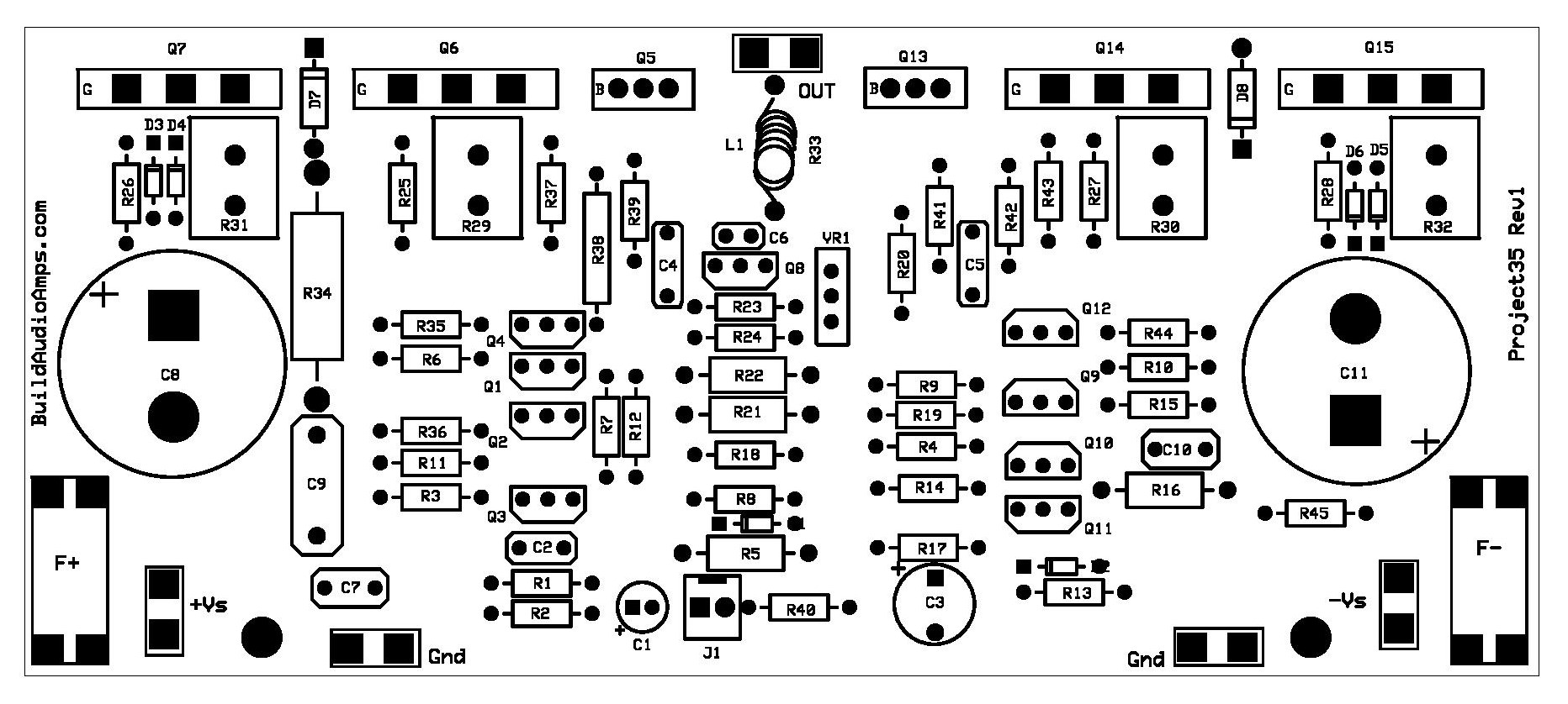
Project 35 Silkscreen Parts Placement Layer of PCB.
If you’ve decided to build this project, the idle current needs to be adjusted first before going any further. Insert a jumper or shunt at the input of the amplifier. Do not connect any load or loudspeaker at the output of the amplifier. Adjust VR1 for maximum resistance of 1KΩ; please refer to the schematic diagram where to access VR1 on top of PCB. Prepare 3 DMMs to measure the DC offset voltage at the output of the amplifier, the voltage drop of the source resistor in any of the power MOSFETs, Q6, Q7, Q14 or Q15 and the overall current across the F+ fuse terminals. Experienced amp builders have more than 3 DMMs.

If a Variac transformer is available, connect the AC input of the power supply to the output of the Variac transformer. Switch the power to ON and gradually adjust the Variac’s AC output from zero until the voltage output of the power supply reaches approximately ±49VDC while keeping an eye on sudden increase in any DMM readings. If you have observed an unusual increase in any of the DMM readings, switch the power to OFF immediately and check the PCB for assembly errors. The picture above shows a DC offset voltage at 2.8mV and could be within ±10mV. The voltage drop across any source resistor is about 20.3mV; readjust VR1 to get a DMM reading from 20mV to 50mV after 10 minutes of warm-up time. The current across the F+ fuse terminals is 131mA; this value is dependent on the adjustment of VR1 and could be from 120mA to 260mA. If you obtain similar DMM readings, you may proceed with music test. One thing you will notice in the music test is that there is no power ON thump and the amplifier is very quiet during the pause between tracks, of course, it’s dependent on how noisy your pre-amp is.
If a Variac transformer is unavailable, make sure that the power supply was properly built and that the output voltage rails have been measured approximately ±49VDC before connecting it to the amplifier project under test. With the power supply at OFF, adjust VR1 for maximum resistance. Switch the power supply to ON; the DMM measuring the voltage drop across any source resistor should read less than 1mV. If the DMM reading is more than 1mV and cannot be adjusted by VR1, power OFF immediately and check the PCB for assembly errors. If the DMM reading is less than 1mV adjust the reading from 20mV to about 50mV after 10 minutes, while the other DMM connected across the F+ fuse terminals, will read about 130mA to 260mA of current. If you obtain similar DMM readings, you may proceed with music test.
To check if the bias was properly adjusted in both initial tests mentioned, switch the project’s power supply to OFF and allow the power amplifier under test to literally cool down for several minutes. With the DMMs in their original test locations, switch the power supply to ON. You will notice that the DMMs measuring the voltage drop across the source resistor and the overall current across the fuse terminals reads high at about 130mV and 600mA or more; please don’t panic, this will happen only when the amp is cold! Allow the amplifier under test to warm-up and stabilized, the DMM readings will eventually go down to about 20~50mV and 130~260mA.
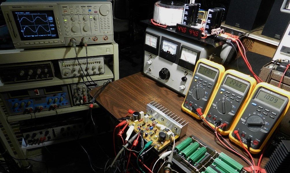
The next test procedure is optional, but if an oscilloscope, audio signal generator and 8Ω dummy load are available, the maximum power output before clipping can be measured. Be careful not to touch the project’s heatsink, it will get very hot during this test!
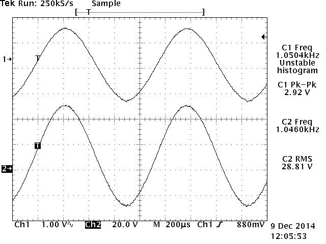
The power output was measured using an HP3312A Function Generator set at 1KHz 2.92Vp-p sine wave output and connected directly to the input of the amplifier under test as well as the CH1 test probe of the oscilloscope. An 8Ω/700Watt dummy load was connected at the output of the amplifier under test as well as the CH2 test probe of the Tektronix TDS520D 500MHz DPO. The power amplifier produces a very nice sine wave of 28.81Vrms across the 8Ω/700W dummy load or a wonderful power output of about 104 Watts, as shown in the TEK hardcopy picture on the right. The oscilloscope’s horizontal scale was adjusted at 200uS to verify for any visible clipping or artifacts on either peak. This power amplifier was paired with a modified LME49720 tone control project; the audio quality reproduced was exceptional.
For more information on HEXFETs, here’s International Rectifier’s Application Note AN-948, it’s a design of a Linear Power Amplifier using complementary HEXFET Power MOSFETs.