Project 44
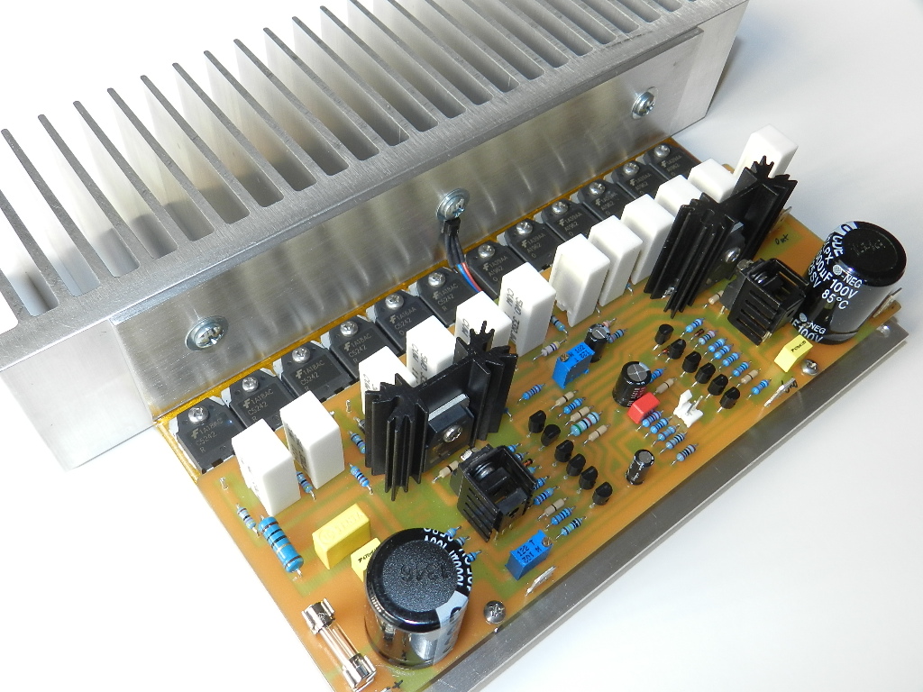
So far, several complementary differential input stage or mirror-image topology power amplifier projects have been presented. Project 44 will be the penultimate complementary differential input stage or mirror-image topology project. Project 44 features a complementary differential input stage, a symmetrical cascode voltage amplifier stage and a three-stage emitter-follower output stage. The project’s prototype produces 45.62Vrms across an 8Ω load or a power output of 260 watts with ±80VDC power supply rails. The project includes six pairs of complementary 17A/250V/130W TO3P power transistors that features wide SOA for reliable operation and excellent gain linearity for low THD from Fairchild Semiconductor.
Here’s a brief description of the circuit:
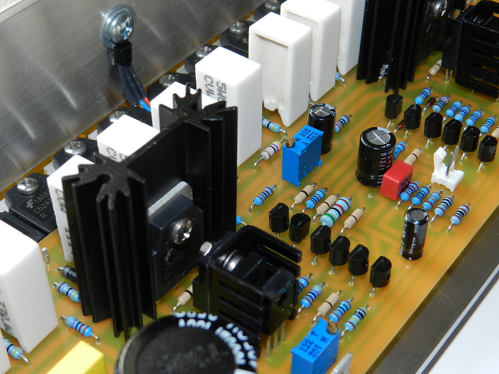
The schematic diagram looks crowded because it is; this power amplifier project is populated with 33 transistors. The input signal from J1 is connected to both complementary differential pairs, Q1/Q2 and Q7/Q8, simultaneously creating a push-pull action. Similarly, a small portion of the output signal is feedback to the inverting input of the differential pairs. To simplify how the circuit operates, only the upper positive half of the schematic diagram will be described because the lower negative half of the circuit is its identical mirror- image.
The positive half of the incoming signal is amplified by Q1 and Q2, forming an input differential current amplifier, current-mirrored by Q3 and Q4 and current-sourced by Q11, Q12, D5 and D6. The output of Q3 is connected to the cascode voltage amplifier transistors, Q13 and Q14. Multilayer ceramic capacitors, C12, C13, C4 and C5 are necessary to compensate for high frequency instability. The very first time the project was powered up, it was drawing too much current from the power supply as indicated by a full scale reading of the AC ammeter of the Variac. Adding C12, C13, C14 and C15 at the voltage amplifier stage transistors prevents the amplifier’s components from breakdown and self-destruction. The output of Q14 is connected to the first emitter follower pre-driver transistor, Q18. It provides some current gain and buffers the output of the VAS from the main driver transistor, Q20, as well. The power output transistor, Q22 through Q27, provides very high current to drive very low impedance loads. A network of L1 in parallel with R61 and C8 in series with R36, also called a Zobel network or sometimes a Boucherot cell, assures the amplifier’s stability when connected to any loads. The overall gain of the amplifier is determined by R23+R33/R7 at 27.25V/V or 28.7dB.
After performing the required initial tests comes what’s considered to be the best part of building this project, the listening test. The prototype unit was connected to a modified LM49720 tone control preamp. While playing “Desire” and “Thanks To You” by Boz Scaggs from his “Dig” album on a Toshiba HD-A2 player and Kenwood speakers, you hear impressive clarity on the vocals, percussions and deep-controlled bass. With the same setup and this time for endurance music testing, the entirety of Safri Duo’s “Episode II” album was auditioned, loudly on the “Samb-Adagio” track. The prototype was also tested with Project 9, the LM1036 tone control project, with very good results.
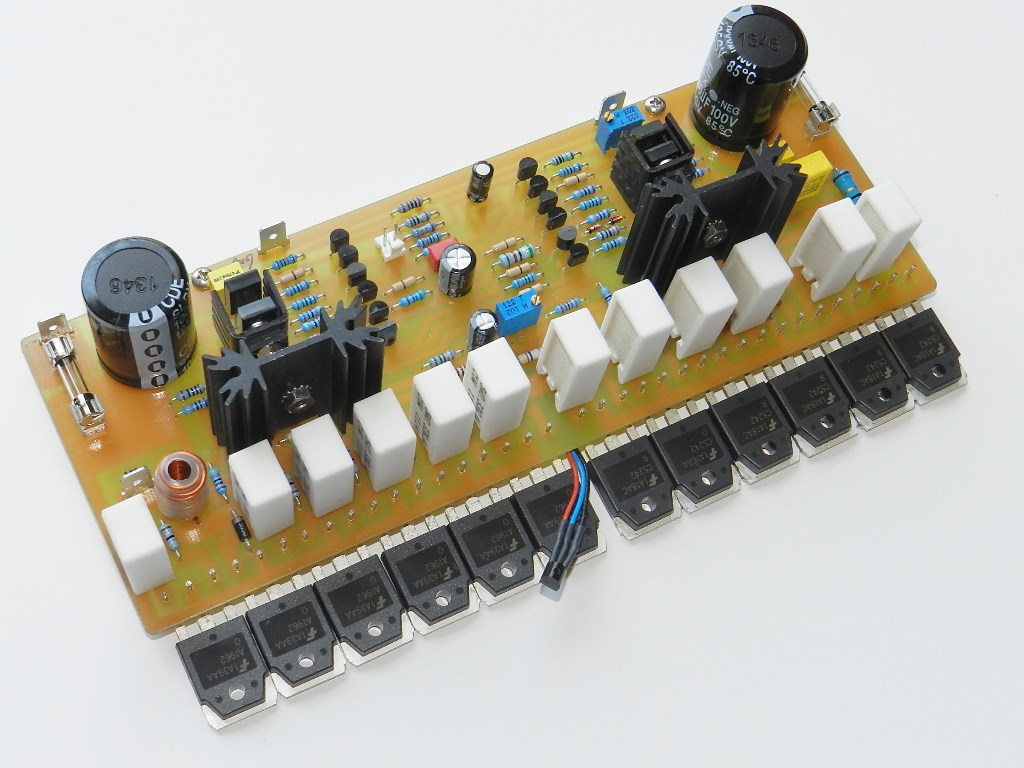
The prototype model was built on an 8” X 3” single-sided PCB. All of the components used in the prototype model are standard available parts. If you are interested in building this project and have read the Information and Policies section of this website, the schematic diagram, PCB layout (available only by request) and BOM are free, as is, no warranty.
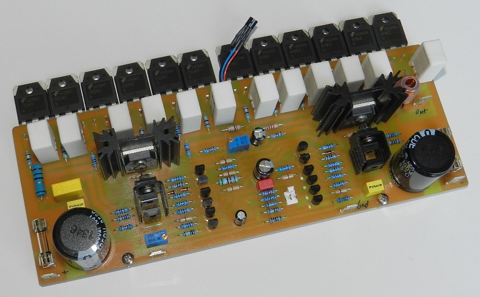
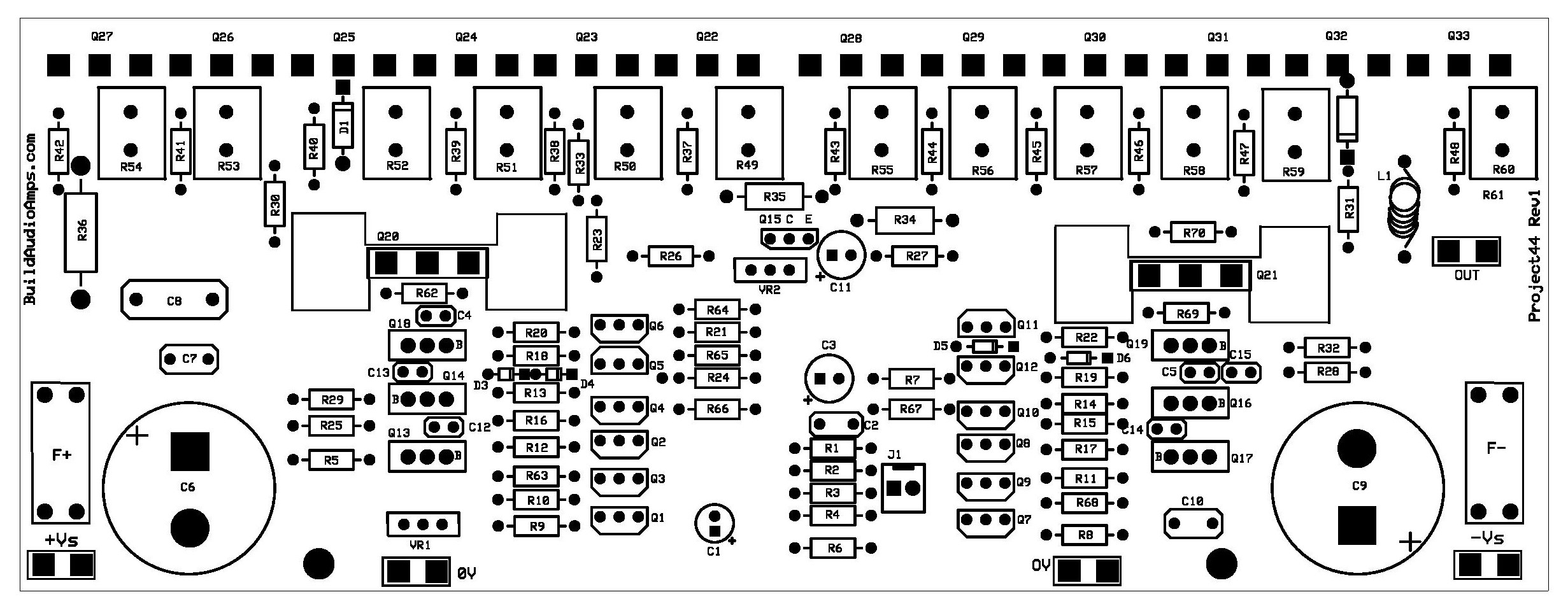 Project 44 Silkscreen parts placement layer of PCB.
Testing the project:
If you have decided to build this project, the DC offset voltage and bias of the power output transistors need to be adjusted first. If you’re installing the project’s PCB similar to the one shown in the following pictures, make sure that the collectors of all power transistors have high or infinite resistance to the metal bracket or heatsink. Q15 is wired and mounted off the PCB with a small piece of double-sided thermal tape similar to those used for attaching a heatsink to CPU, GPU or RAM in computers. The recommended power supply for this project is from ±64VDC to ±80VDC at 3A to 6A obtained from a rectified and filtered 110VCT to 116VCT power transformer. Make sure that power supply has been properly built and it’s output rails measured before connecting it into the amplifier.
Install a shunt or short at the input of the amplifier. Adjust VR2 to its maximum resistance of 1Kohms. VR2 can be accessed on top of the PCB at R26 and R27, please refer to the schematic diagram. Do not connect any load or loudspeaker at the output of the amplifier. Make use of several test clips to temporarily connect the amplifier to the power supply and DMMs for testing.
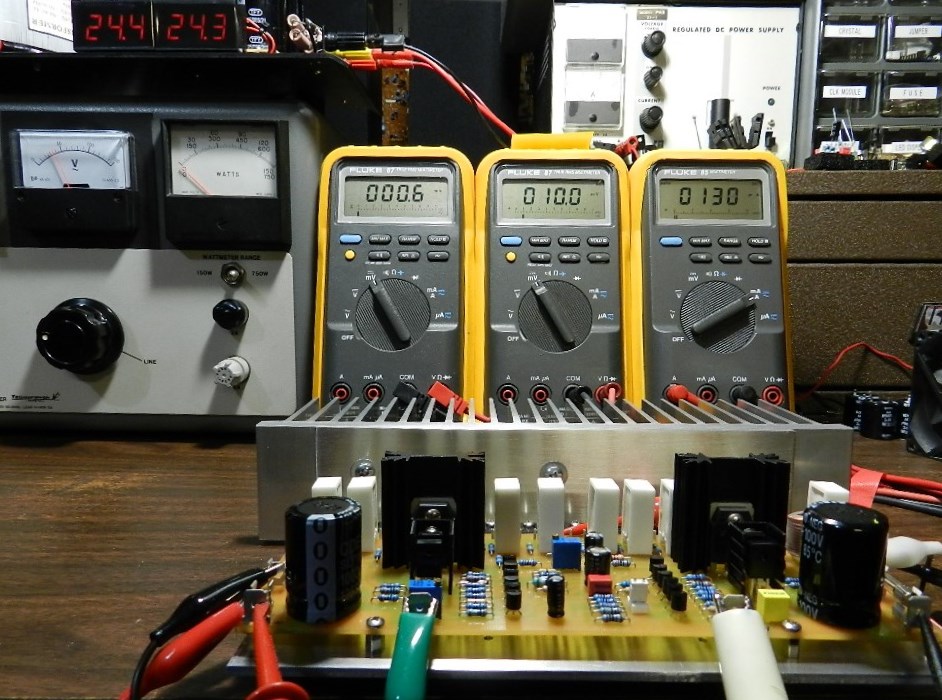
The picture on the left side uses ±24VDC power supply rails for initial testing. The DMM on the left side is reading 0.6mV, the DC offset of the amplifier and this can be adjusted by VR1 within ±10mV. The DMM in the middle is reading 10mV, the voltage drop across R54 and R60. At power ON, it should measure less than 1mV, if not, power OFF immediately and check to PCB for assembly errors. The black test probe of the DMM is connected to the emitter of Q33 and the red test probe at the emitter of Q27. Adjust VR2 to get to this value and it could be anywhere from 5mV to 10mV after a warm-up period of 10 minutes. The DMM on the right side of the picture is reading the current across the F+ fuse terminals at 130mA. This reading is dependent on the adjustment of VR2.
If you have obtained the same DMM readings as described, readjust VR2 for minimum DMM reading. Switch the power to OFF and you may proceed with the next test at this time using ±80VDC rails. Be careful not to touch any component in the PCB when performing this test.
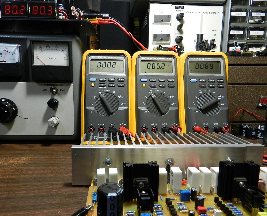
The picture on the right uses ±80VDC power supply rails. The DMM on the left side of the picture is reading the DC offset voltage at 0.2mV. This can be adjusted by VR1 within ±10mV. The DMM in the middle is measuring the voltage drop across R54 and R60 at 5.2mV. This can be adjusted by VR2 from 5mV to 10mV. The DMM on the right is measuring the current across F+ fuse terminals (fuse removed, of course) at 89 mA. If you get the same DMM readings, proceed with music test. This project was also auditioned with the LM1036 tone control Project 9!
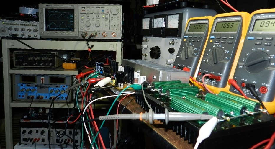
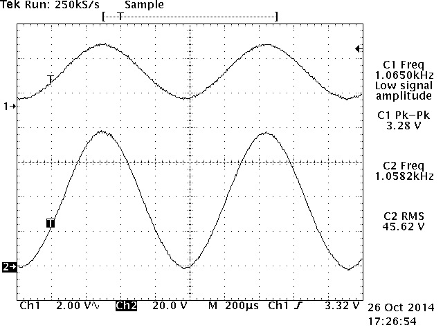
The next test is optional, but if an oscilloscope, function generator and a high-wattage 8Ω dummy load are available, the maximum power output of the amplifier can be measured before clipping occurs. Be careful not to touch the heatsink or the dummy load during the test, they will get extremely hot! The HP3312A function generator was set for a sine wave output of 1KHz at 3.28Vp-p and connected directly to J1, as well as CH1 probe of the Tektronix TDS520D 500MHz oscilloscope. An 8Ω/700watt dummy load was connected at the output of the amplifier as well as the CH2 probe of the oscilloscope. The amplifier produces 45.62Vrms across the 8Ω/700W dummy load or a power output of 260 watts or more than 500 watts when connected with a 4Ω load. The scope’s horizontal scale was adjusted at 200uS to verify for any signs of clipping or artefact in both peaks of the output waveform. Enjoy!