Project 62
Project 62 is the first in the series of audio power amplifier projects that uses an op-amp in the front-end input stage. This project is based on a “Build This” article written by Reinhard Metz that was published in April 1992 issue of the Radio Electronics magazine. Although the construction plan of the project is more than 20 years old, the output stage section of the project is an interesting design. The input stage is a JFET operational amplifier while the driver and power output stages are using discrete devices. The BJT driver transistors are coupled to the paralleled-complementary power MOSFETs. The output of the amplifier is connected to all the drain terminals of the power MOSFETs, similar to a CFP topology. The stability of the amplifier in this type of design is made possible by introducing a local feedback loop with a gain of 15 between the driver and output devices. A small amount of output signal is also applied to the inverting input of the opamp to provide a negative feedback with a gain of about 51. There’s a reason for doing this arrangement because if the op-amp is left unaided there’s no way that the overall power output signal could swing near to the project’s power supply rails.
Fortunately, Reinhard Metz had agreed to have his design revisited and shared here. He did mention, “I'm one of the minority supporters of common drain design with gain in the output stage and have had good results with that approach”. By searching the Internet you can still find, read and analyze several of his designs, but he also maintains his own website at http://www.a-and-t-labs.com/products.htm.
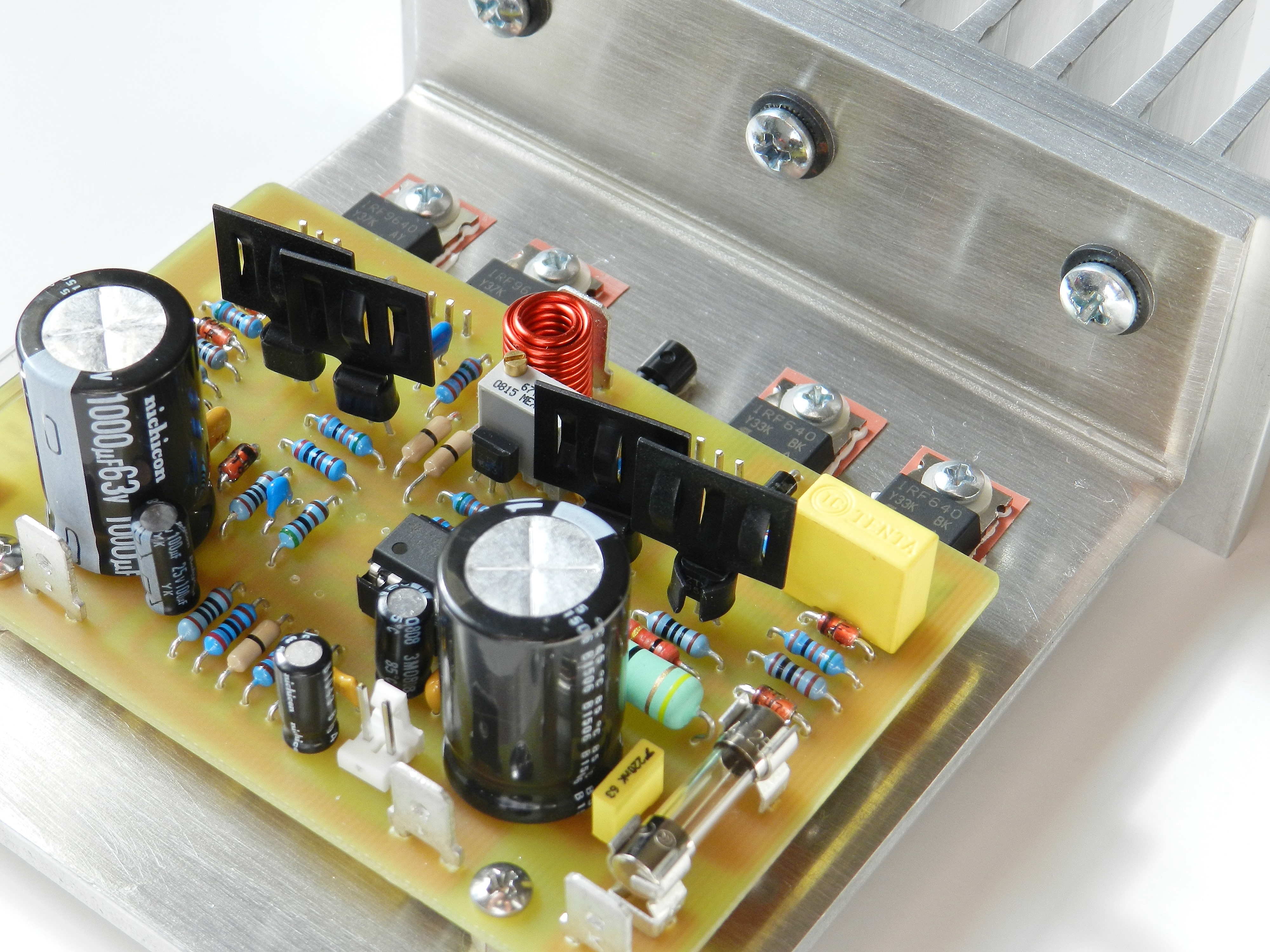
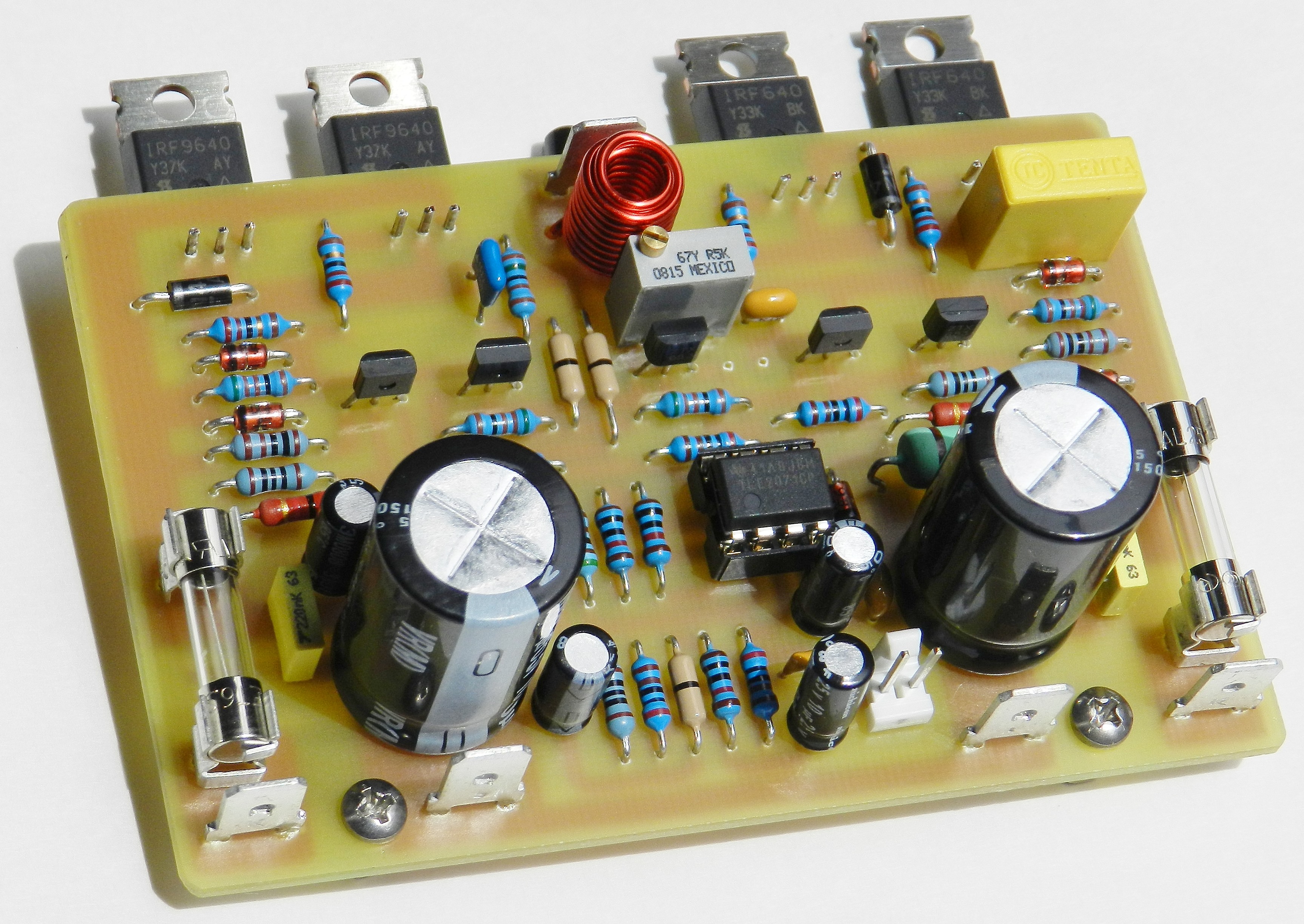
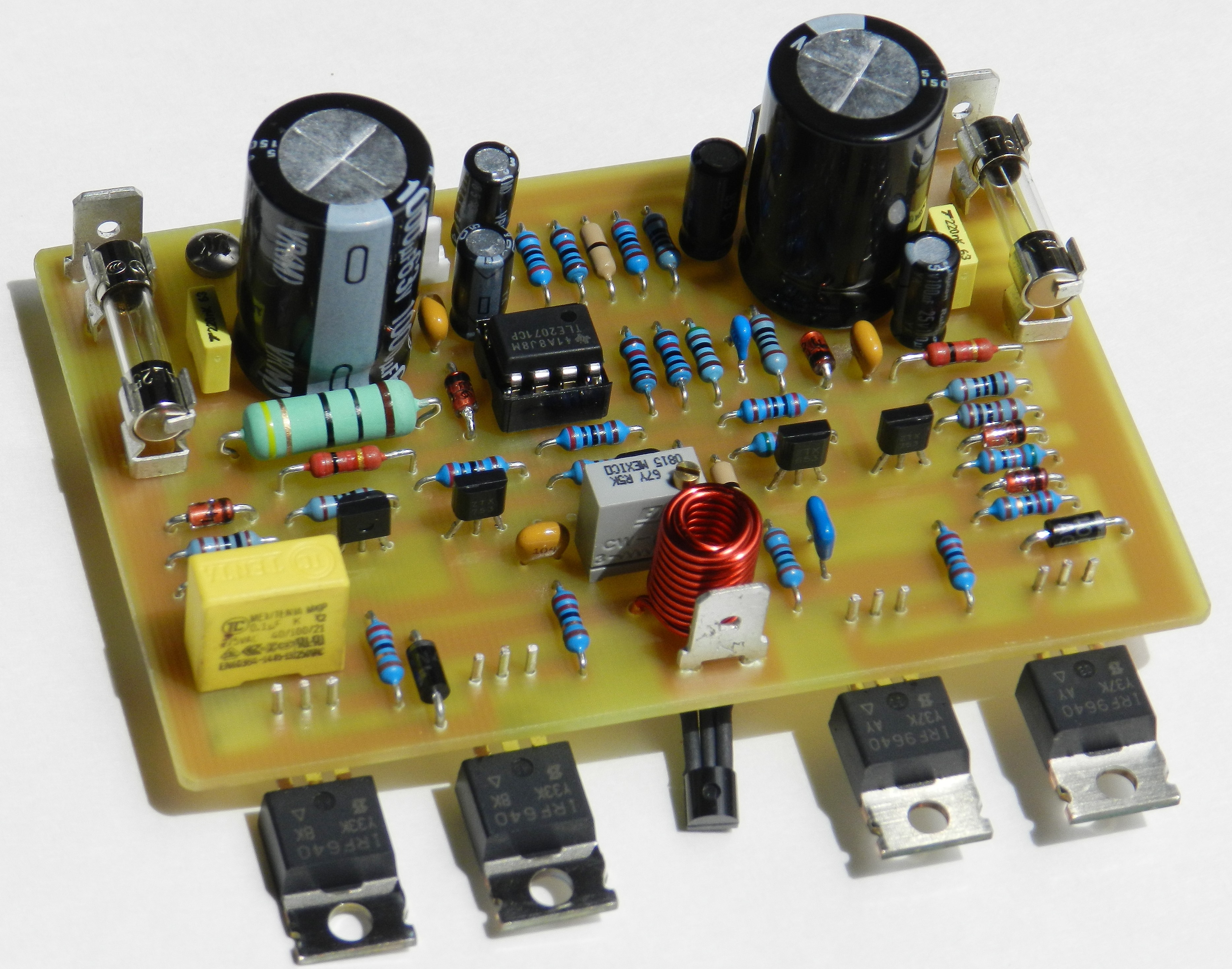
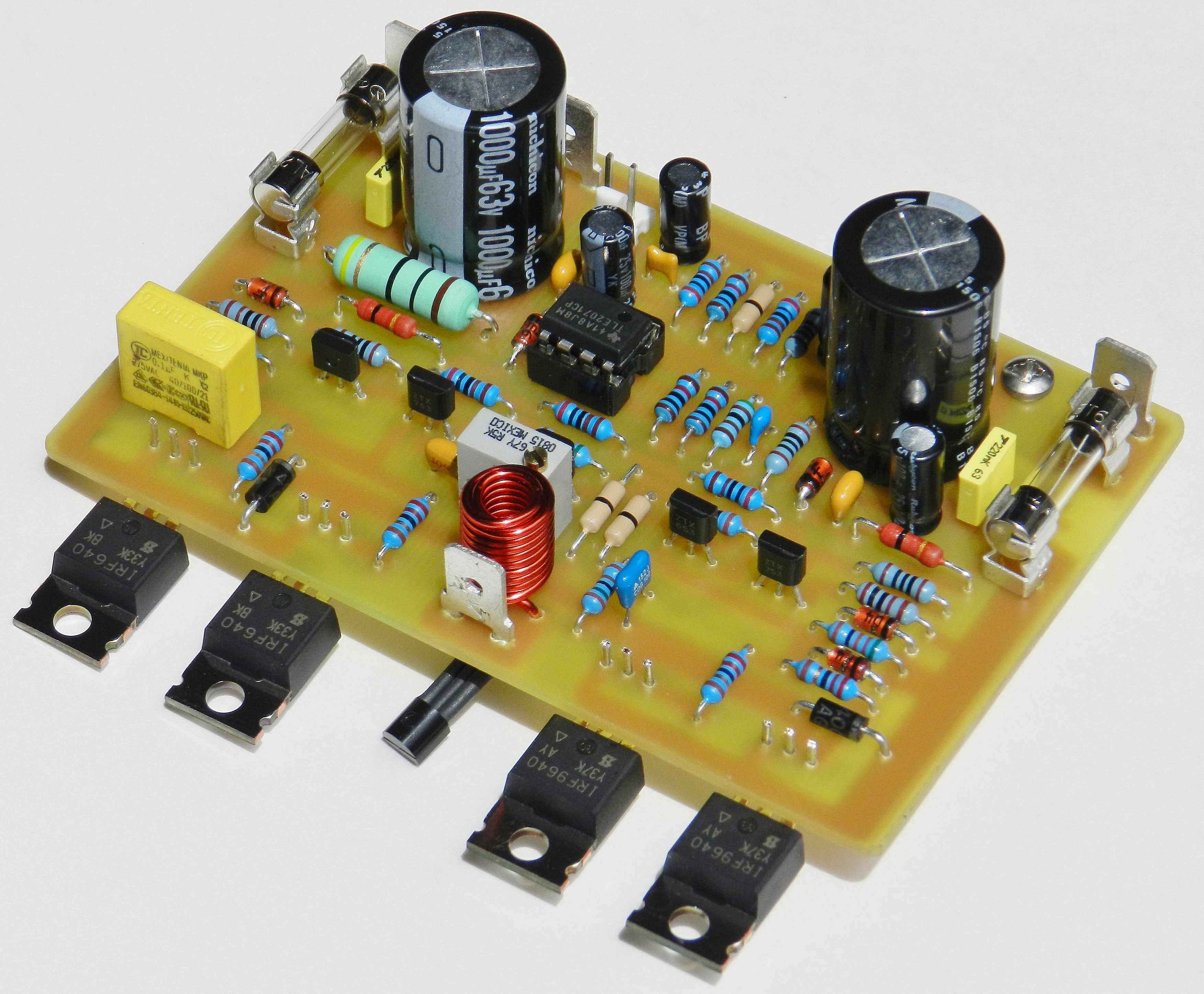
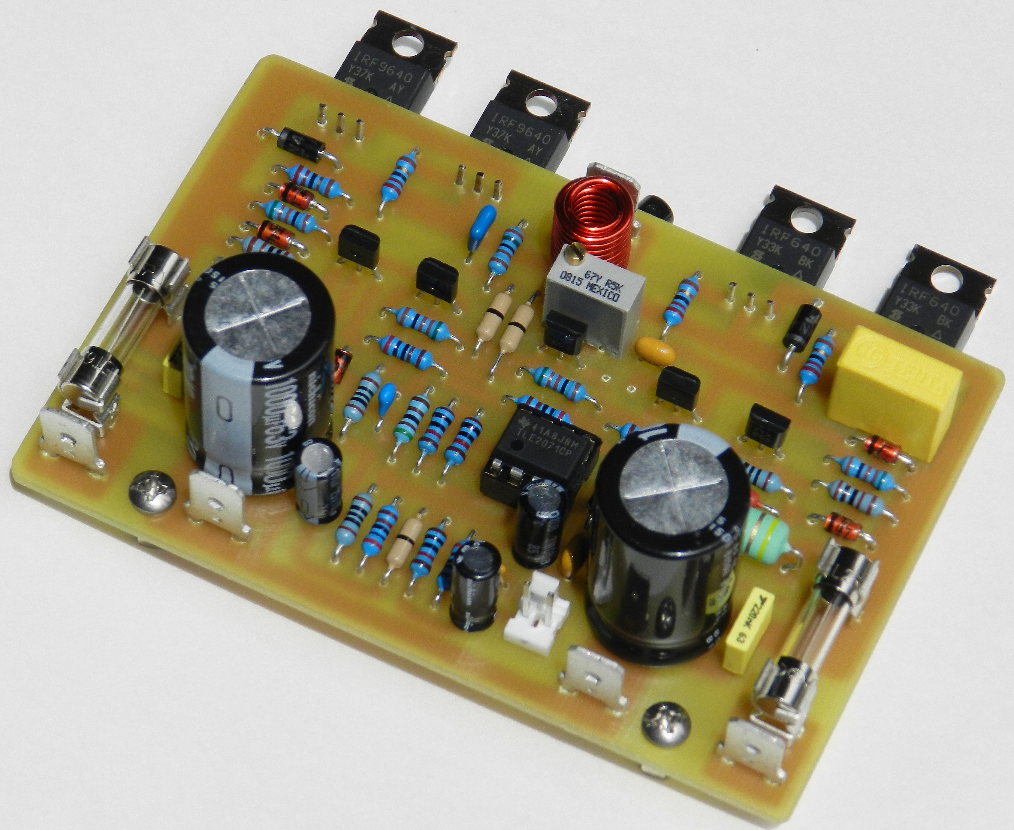
The article’s original schematic diagram has been redrawn to include some modifications, which in my opinion improves even more the performance of the amplifier. The redrawn schematic diagram will be referred to from hereon and is found here. The PCB layout was created using the ExpressPCB software, laser-printed and then etched into a 3.8” X 2.5” single-sided PCB. The header pictures above shows the PCB revision at Rev1 while Figures 1 and 2 shows the PCB revision at Rev2. The revision change made was the omission of two null offset resistors in the original schematic diagram. The completed and fully tested module is shown in the bottom footer pictures.
The power output of the amplifier is about 113watts at 8Ω with a ±45VDC power supply rails. The power output rating was acquired by measuring the voltage across the 8Ω dummy load when a 1KHz 0.495Vrms sine wave signal is applied to the input of the amplifier. The QA400 audio analyzer measured the THD from 0.001% to 0.009% depending on the op-amp used.
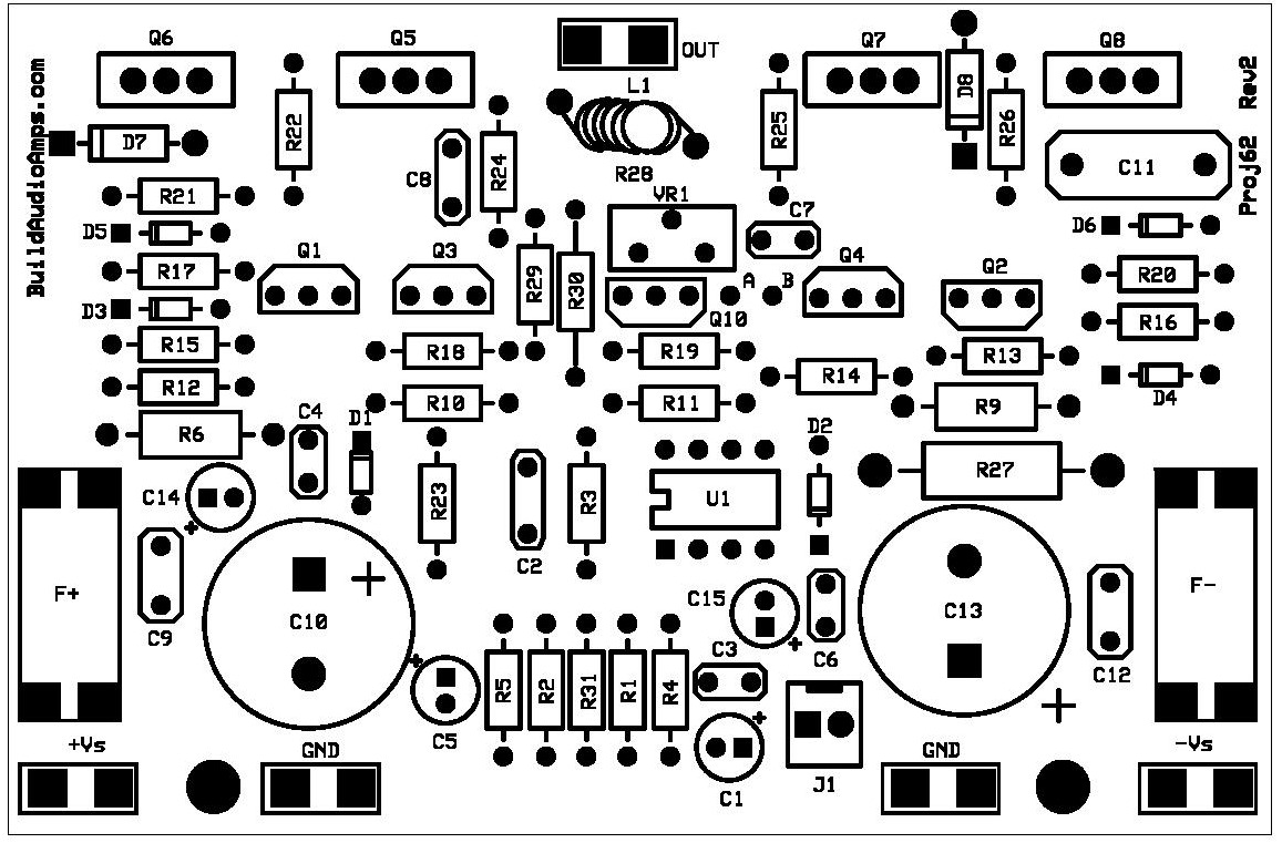
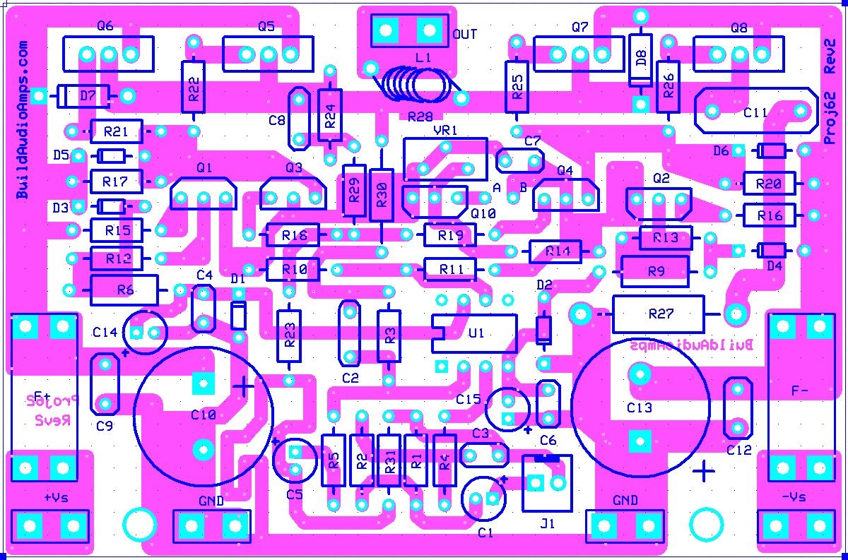
Figure 1. Silkscreen, pads and text layer of Project 62’s PCB. Figure 2. A see-through top and bottom layer of the PCB.
The prototype’s op-amp, U1, features better overall performance than the op-amp used in the original design. Texas Instruments called it the “Excalibur Low-Noise High-Speed J-FET input” op-amp. An 8-pin IC socket was intentionally populated in the prototype so that other types of op-amps may be tried out and tested, which will be shown later. The null offset resistors connected at pins 1 and 5 to Vcc were removed because U1 already features an internal zener trimming of the offset voltage. According to TI, the on-chip zener trimming of offset voltage yields precision grades for greater accuracy in dc-coupled applications. Initial testing of the amplifier shows the DC offset voltage is held at zero volts all the time whether J1 is open or shorted.
The general purpose small signal transistors used in the current source/sink and driver stages are no longer available from Fairchild Semiconductor. Instead, they were substituted with 100V, 2A, 1W medium power transistors in a TO92-compatible E-Line series from Diodes Inc. TO-92 heat sinks by Aavid Thermalloy (P/N 575200B00000G) were mounted into these transistors to improve heat dissipation. The heat sinks made their package temperature no higher than 55˚C. The surface area of the copper traces around these transistors was also made larger as suggested by Diodes Inc.
Additional decoupling capacitors, C14 and C15, were populated across D1 and D2 respectively, improving the opamp’s ability to reject, if any, ripple or fluctuation voltage present in the power supply rails. Also included is an output filter network consisting of R27, R28, L1 and C11 which improves the overall high frequency stability of the amplifier when connected to different types of loads. Diodes, D7 and D8, connected at the supply rails to the output of the amplifier clamps any output beyond +Vs and -Vs mainly caused by loudspeaker excursions or speaker coil inductance. There is no protection circuit included but the “uPC1237 Speaker Protection and Power ON Delay Project” could easily be implemented into the project for peace of mind.
It was suggested to match each type of paralleled power MOSFETs so that there is equal current sharing and power dissipation. A simple MOSFET matching circuit can be built on a breadboard (shown here and here) to measure the gate voltage (VGS) and drain current (ID). Each device should be matched within 3.728V of gate voltage to produce a drain current of 50mA and a gate voltage of about 4.06V for a drain current of 200mA. See the power MOSFET specs and the MOSFET matching circuit notes for additional information.
Figure 3. Initial test setup of the completed amplifier project.
The initial test setup and DMM measurements of the prototype is shown in Figure 3. Before applying power to the amplifier, VR1 should be adjusted to minimum resistance and you should not insert any op-amp in the IC socket. With the ±45VDC power supply rails connected, the voltage across D3 and D4 should be about 6.2 volts and across D1 and D2 should be about 15 volts. If all the voltages are present, switch off the power and wait until the power supply’s filter capacitors are completely discharged. Insert U1 into the IC socket and then re-apply power to the amplifier.
The DMM on the left is connected at the output of the amplifier and measures the DC offset voltage at 0 mV. The DMM on the right is connected across the F+ fuse terminals and measures the total current drawn by the amplifier at 60mA. Carefully adjust VR1 to get to this reading. Verify the voltage between the bases of Q3 and Q4 should be about 7.6 volts. You may proceed to the listening test if the same measurements were achieved, otherwise you may perform the next optional tests if the test equipments are available.
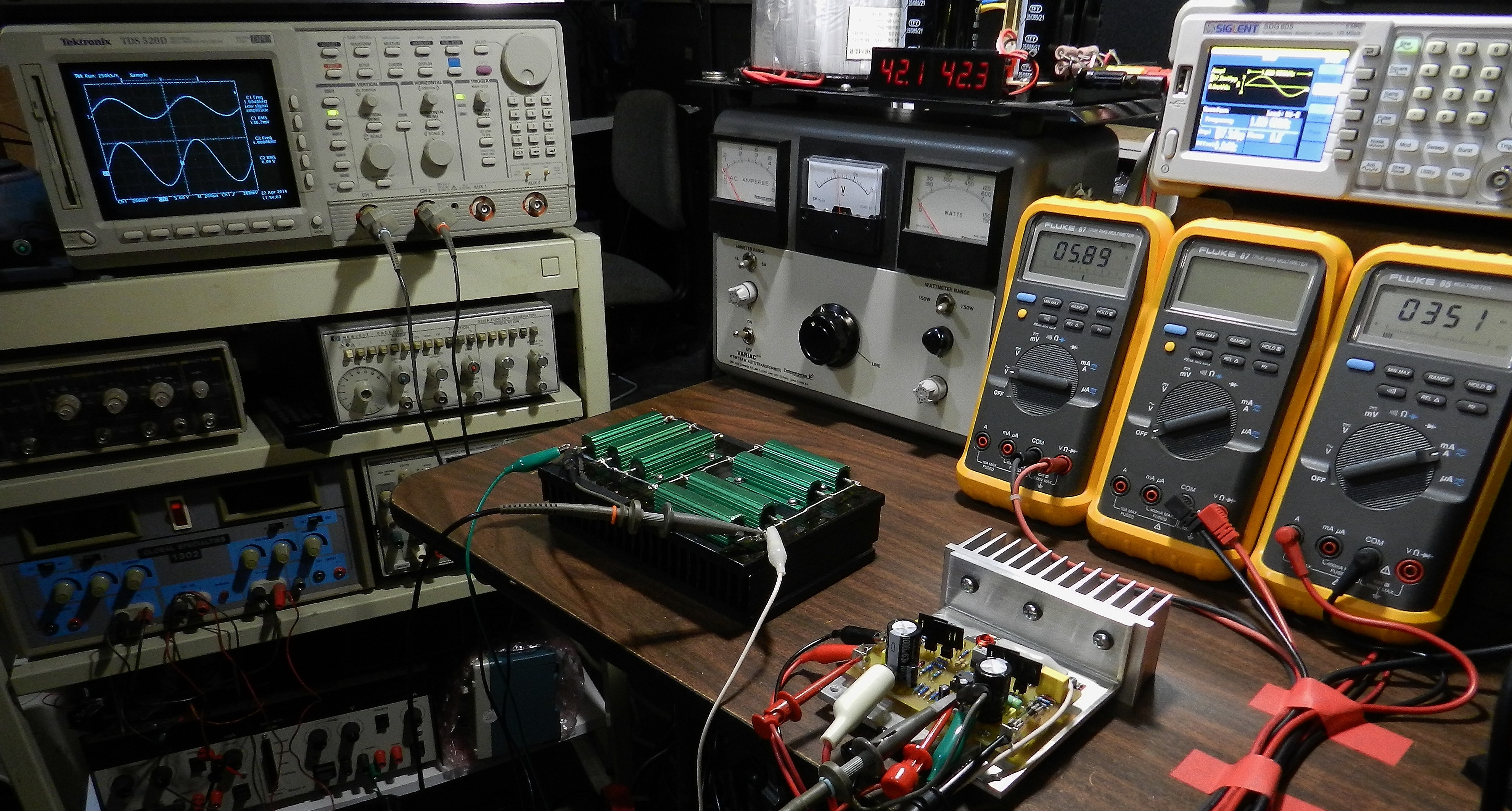
Figure 4. Power output and square wave response test measurement setup.
The power output and square wave response test setup is shown in Figure 4. A hardcopy of the test result for power output measurement is shown in Figure 5. As you can see, the amplifier requires only about half a volt of input signal to produce the full rated power output before clipping occurs. The 1KHz square wave response test result in Figure 6 also shows the rise and fall times of the waveform. The prototype was also tested with 20Hz and 20KHz square waves.

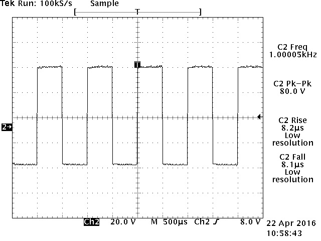
Figure 5. Power output measurement test result. Figure 6. 1KHz square wave response test result.
There are two frequency-compensating capacitors in the design that allows you to adjust and experiment the tone profile of the amplifier. Increasing the capacitance of C8 allows you to increase the high frequency response of the amplifier and vice versa. The other capacitor is C2; by replacing its value from either higher or lower, affects the low frequency response of the amplifier. It is up to the builder to experiment with the tone characteristic of the amplifier but, as it is, in my opinion, the project sonically performs very well and is perhaps one of the best sounding amplifiers in the 100-watt category.
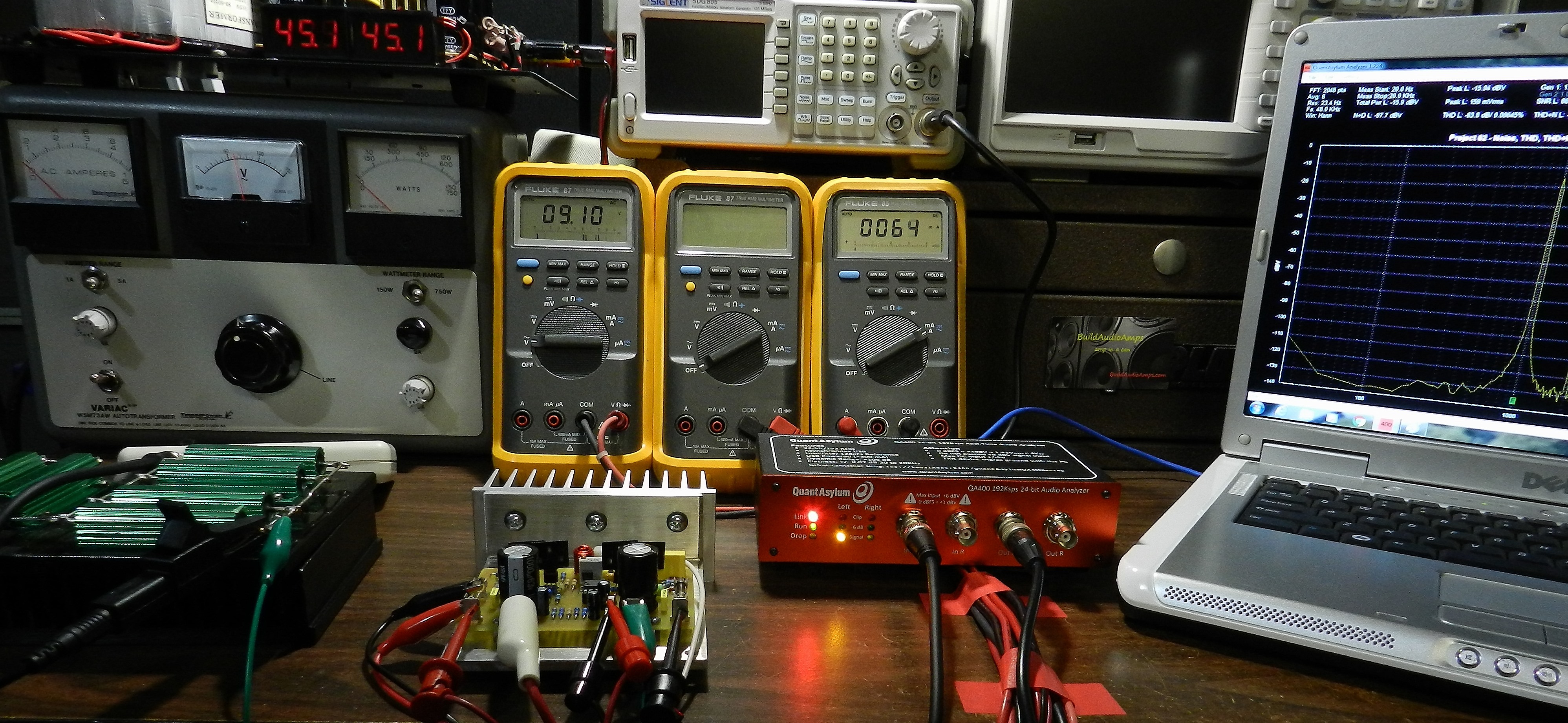
Figure 7. QA400 audio analyzer test setup.
Figure 7 shows the test setup of the QA400 audio analyzer. The audio analyzer test setup consists of a QuantAsylum’s QA400 USB audio analyzer, QA190 low-noise differential probe, 8Ω dummy load and a PC laptop to measure the following: Noise, THD, THD+N, SNR and the frequency response of the amplifier. Figures 8 through 11 shows the acquired Noise, THD, THD+N and SNR test results. Different types of opamps were tested as follows: OPA604, TLE2071, TL071 and TL081. The best test result is the one using OPA604, however, there are other op-amps available in the market that have better specifications and may be used in the design -if your budget allows.

Figure 8. QA400 test results using OPA604 OpAmp.
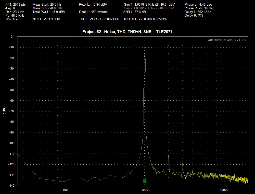
Figure 9. QA400 test results using TLE2071 OpAmp.

Figure 10. QA400 test results using TL071 OpAmp.

Figure 11. QA400 test results using TL081 OpAmp.
How does this project perform in music listening test? Playing with different CD album genres, the listening experience was very impressive. The prototype unit was connected to a modified LM49720 tone control preamp, a Toshiba HD-A2 player, several test speakers and finally into a Bose Acoustimass 3 Speaker System with their inputs paralleled. Listening to Daft Punk’s multi-award winning “Random Access Memories” album, you hear deep controlled bass, extended highs and impressive mids as well, especially from the cut entitled “Doin’ it Right”. Also listened to a DDD recording of Vivaldi’s “Four Seasons”, this time focusing your perception to the accurate sound reproduction of the Adagios. Overall, granting that the audio power amplifier design was developed 24 years ago to date, the revisited project did not disappoint but rather resulted into an exciting build after all!