
Project 15

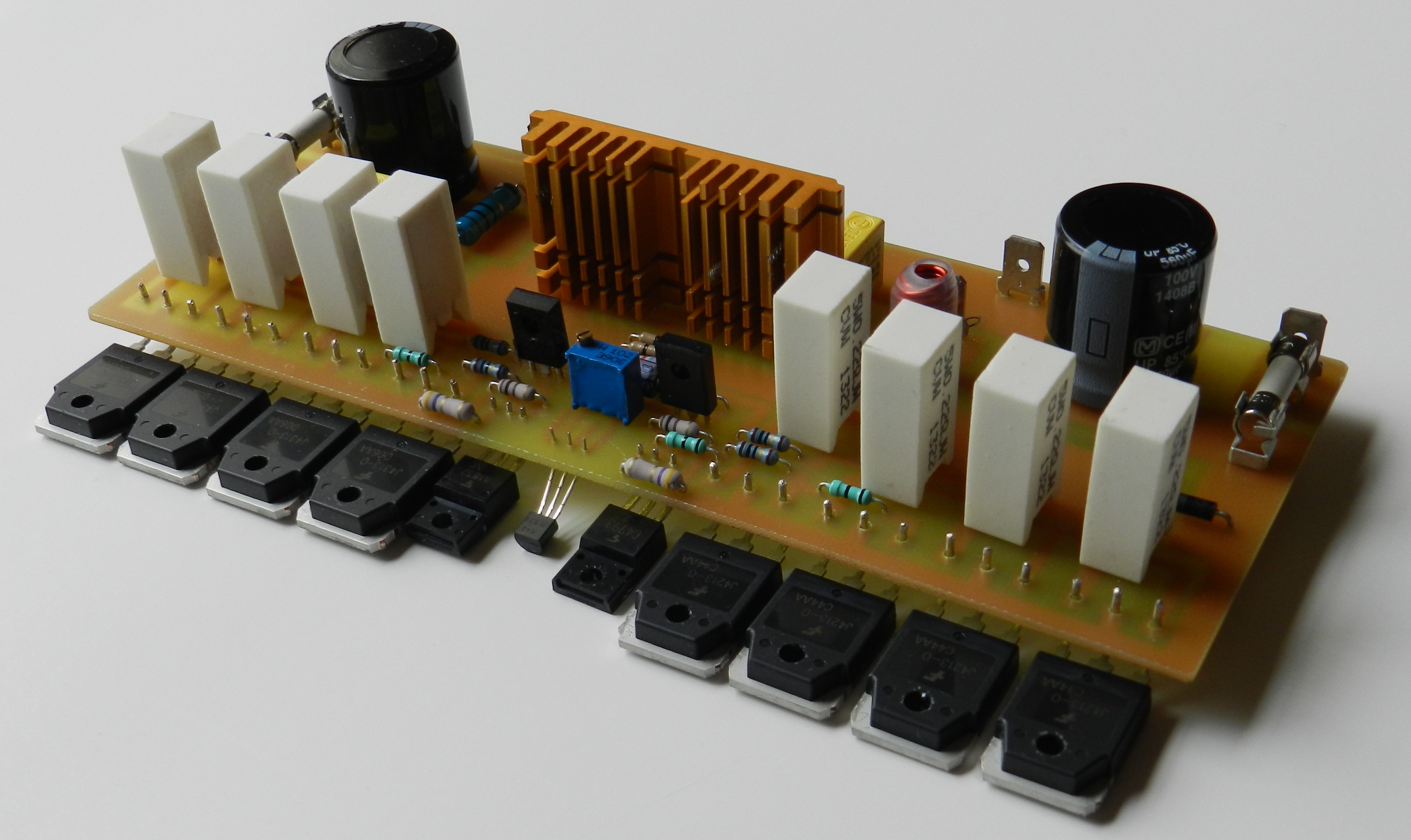
The driver stage of Project 15 is a complementary feedback pair (CFP) configuration also known as the Sziklai pair, named after its inventor in the early 50s, George Sziklai. This 2-BJT configuration is similar to Darlington but the Sziklai uses a complementary transistor pair. Only a few audio electronics manufacturers use Sziklai-based designs compared to Darlington-based designs. The Crown XLS series and C-Audio Pulse series uses identical Sziklai-based driver stage circuits. However, to make their circuits work for this project, R9/R10 and R25/R26 have to be added, just like in the Citation22 from Harman Kardon.
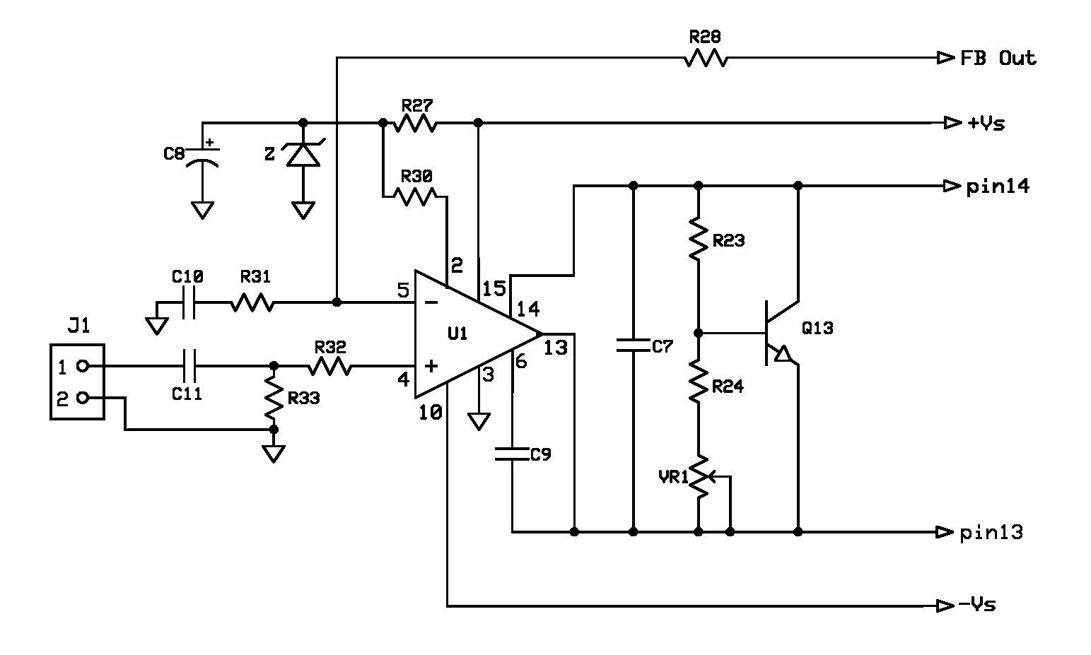
Transistors Q1/Q2 and Q7/Q8 are Sziklai-configured emitter-follower for the power output transistors Q3 to Q12. Transistors Q1/Q7 can be 2SD669/2SB649 but the actual part values are listed in the BOM. The 2SC3503/2SA1381 transistor pair was tested but awful oscillations occurred. The addition of bypass resistors R18/R19 in the Sziklai-pair improves stability and performance. C12 was added to Q7 to improve high frequency stability. In the final tested model, a small heat sink was attached to Q1 and Q7 for improved heat dissipation of the device. The measured power output of Project 15 is about 140Watts rms at 8Ω with a power supply of ±54VDC. Here’s the schematic diagram of the LME49811 input stage circuit:
The original value of resistors R28 and R33 were changed and determined by t&e, to match with the output stage circuit. A couple of SMDs were combined with the rest of the through-hole components to simplify copper trace runs on the PCB layout and challenging to build! The SMD types are noted in the Part Value column of the bill of materials and matches with the Part IDs on the PCB. If you plan to build this project, the output stage schematic diagram, the PCB layout as well as Project15 BOM are provided for free by request, as is, no warranty.
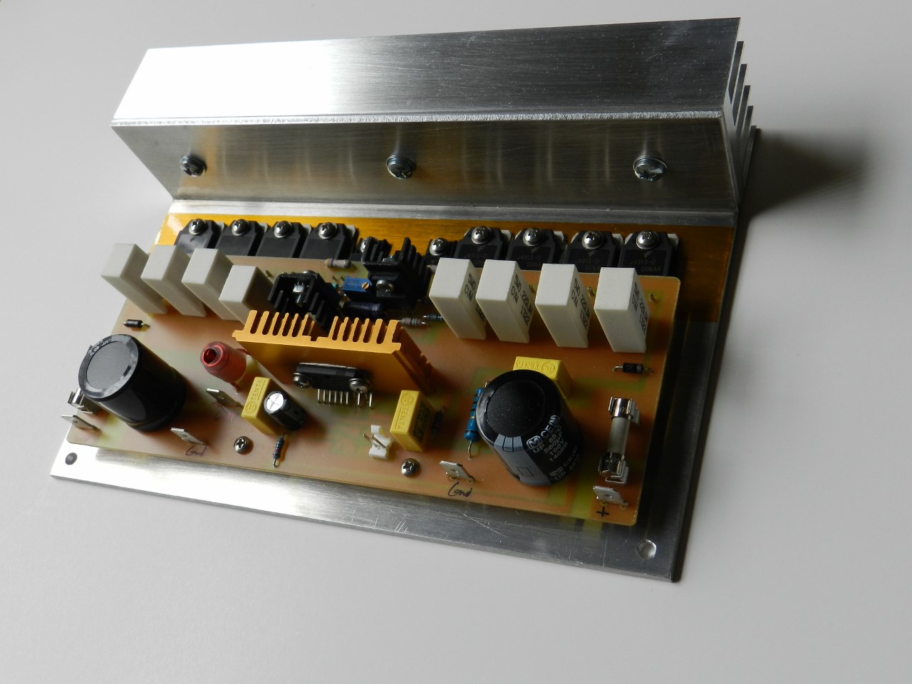
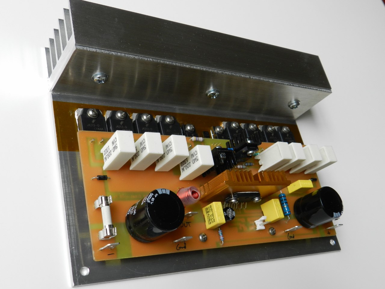
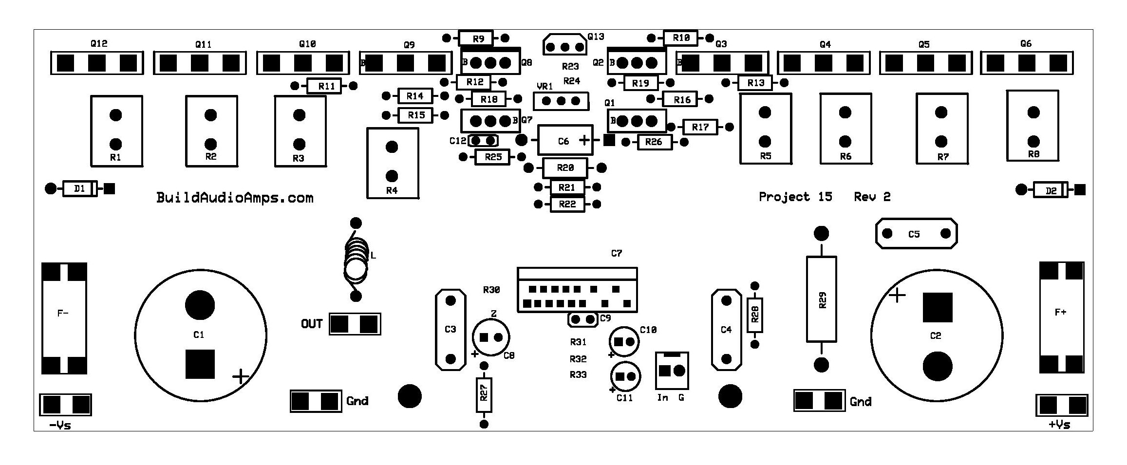 Silkscreen Parts Placement Layer of PCB for Project 15
To finish up the project, the idle current of the power output transistors needs to be adjusted first, before you proceed with music test. Install a shorting jumper at input J1 and do not connect any speaker yet. Adjust VR1 clockwise until it clicks. Connect a millivoltmeter at the output and ground PCB terminals to measure the DC offset voltage of the amplifier. Remove F+ fuse, if installed, and insert a milliammeter at its PCB terminals to measure the current drawn by the amplifier. Connect another millivoltmeter at the emitters of Q9 and Q3 to measure the voltage drop across R4 and R5 (see the red and black test clips in the following picture). If a ±24VDC power supply is available use that to power up the project the first time, just to be safe! Switch the power supply to ON and wait for about 15 minutes before adjusting VR1.
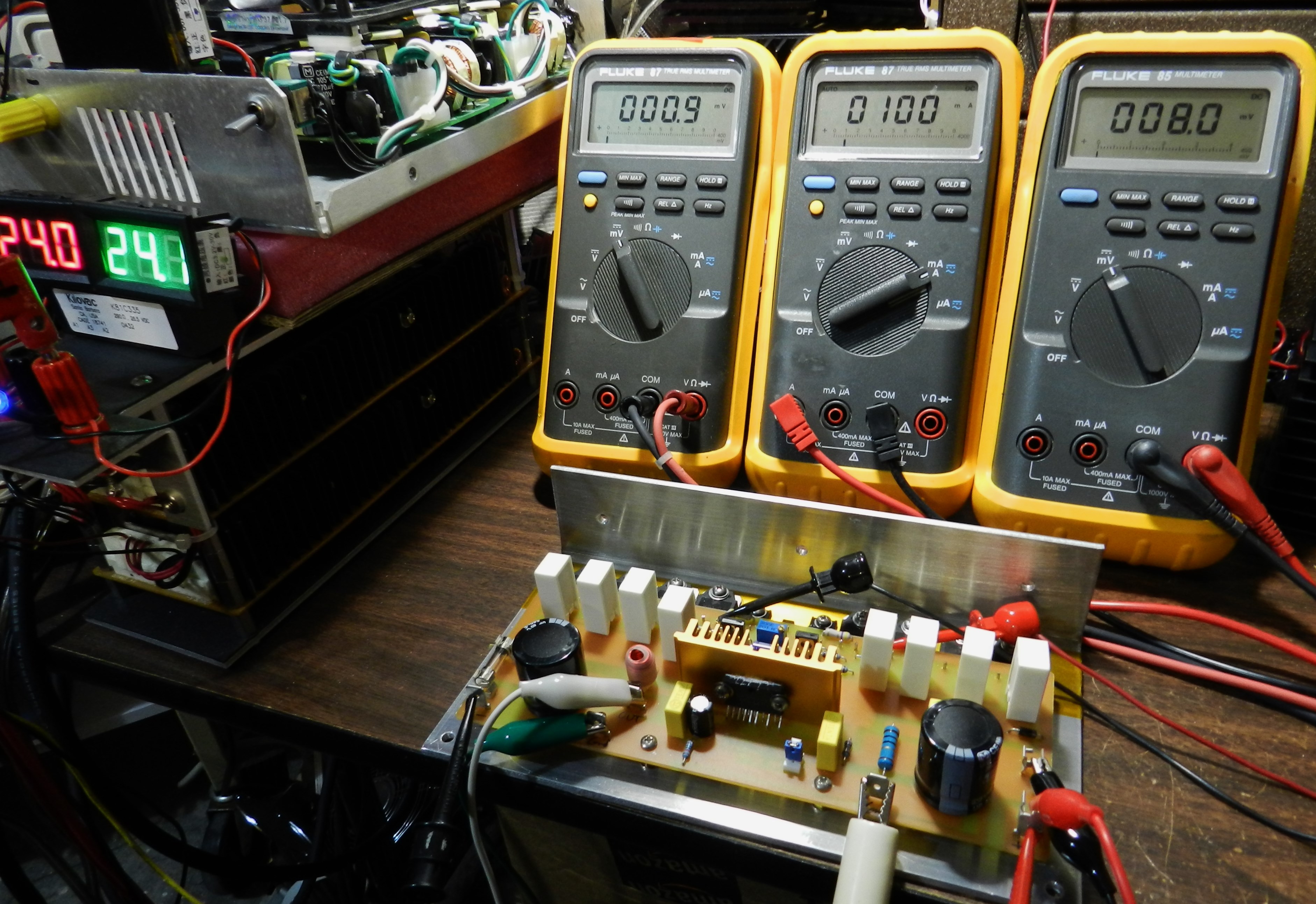
The DMM on the left side of the picture is reading 0.9mV the DC offset voltage of the amplifier. The DMM in the middle is reading 100mA, the current drawn by the amplifier. The DMM on the right side of the picture is reading 8mV, the voltage drop across R4 and R5. Adjust VR1 counterclockwise to obtain 8mV. The voltage drop reading on the DMM multiplied by the emitter resistance values is the idle current of the power output transistors. Readjust VR1 if necessary. If you obtain different DMM readings, switch OFF the power supply immediately and check for assembly errors. If you got it right, proceed with music test!
The next test procedure will be using a ±54VDC power supply. All the DMMs are connected the same way as in the previous tests. Adjust VR1 clockwise until it clicks. Install a shorting jumper at input J1 and do not connect any speaker yet. Switch power supply to ON and wait for about 15 minutes before adjusting VR1.
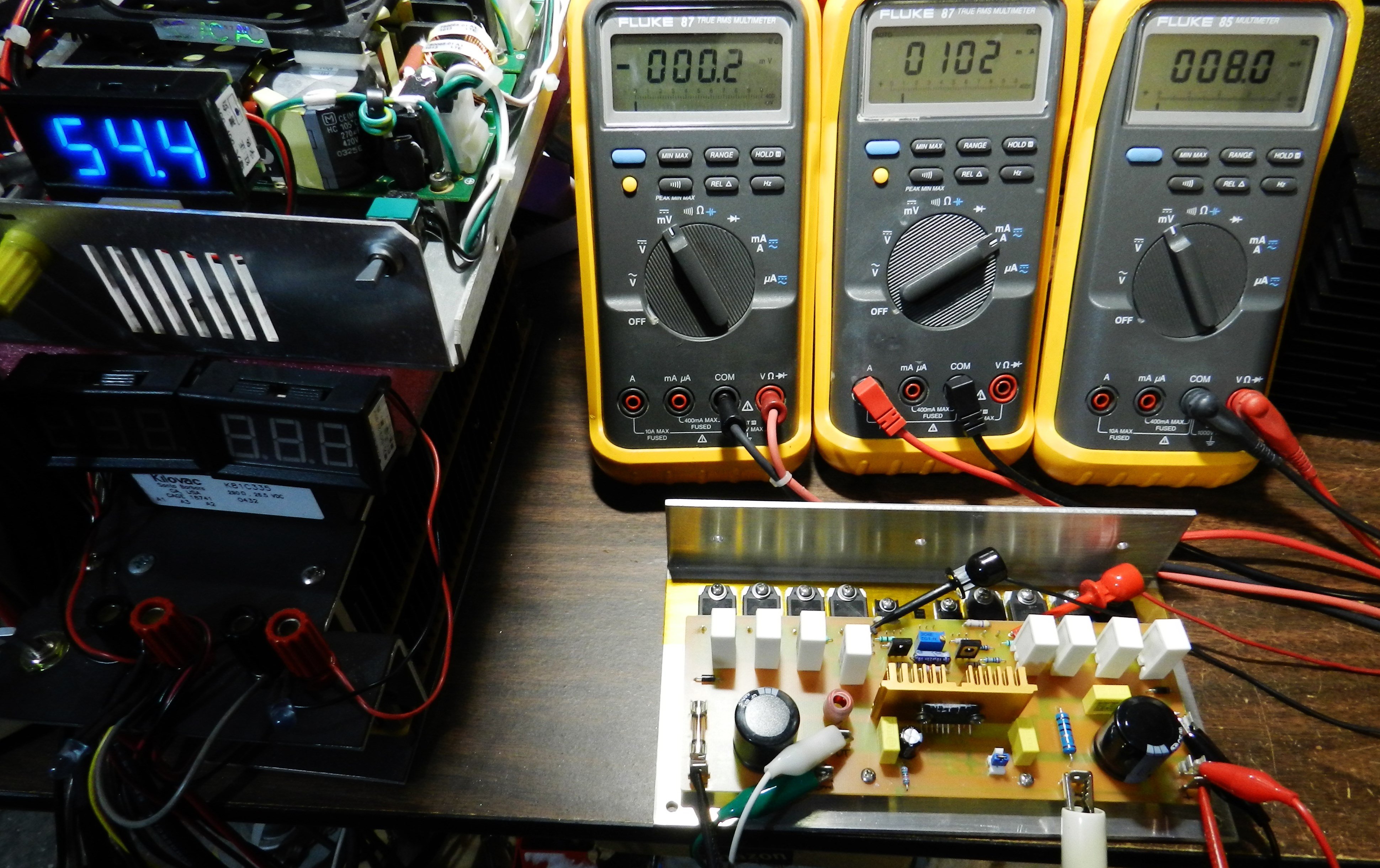
The DMM on the left side of the picture is reading 0.2mV, the DC offset voltage of the amplifier. The DMM in the middle is reading 102mA, the current drawn by the amplifier. The DMM on the right side of the picture is reading 8mV, the voltage drop across R4 and R5. Adjust VR1 counterclockwise to obtain 8mV. The voltage drop reading on the DMM multiplied by the emitter resistance values is the idle current of the power output transistors. Readjust VR1 if necessary. Other than those DMM readings, power OFF immediately and check for PCB assembly errors. If not, proceed with music test.
The next step is optional, but if you have an oscilloscope, audio signal generator and an 8Ω dummy load, the power output of the amplifier under test can be measured. It is recommended to add a small fan, to cool down the amplifier under test and dummy load. Be careful, they will get hot!
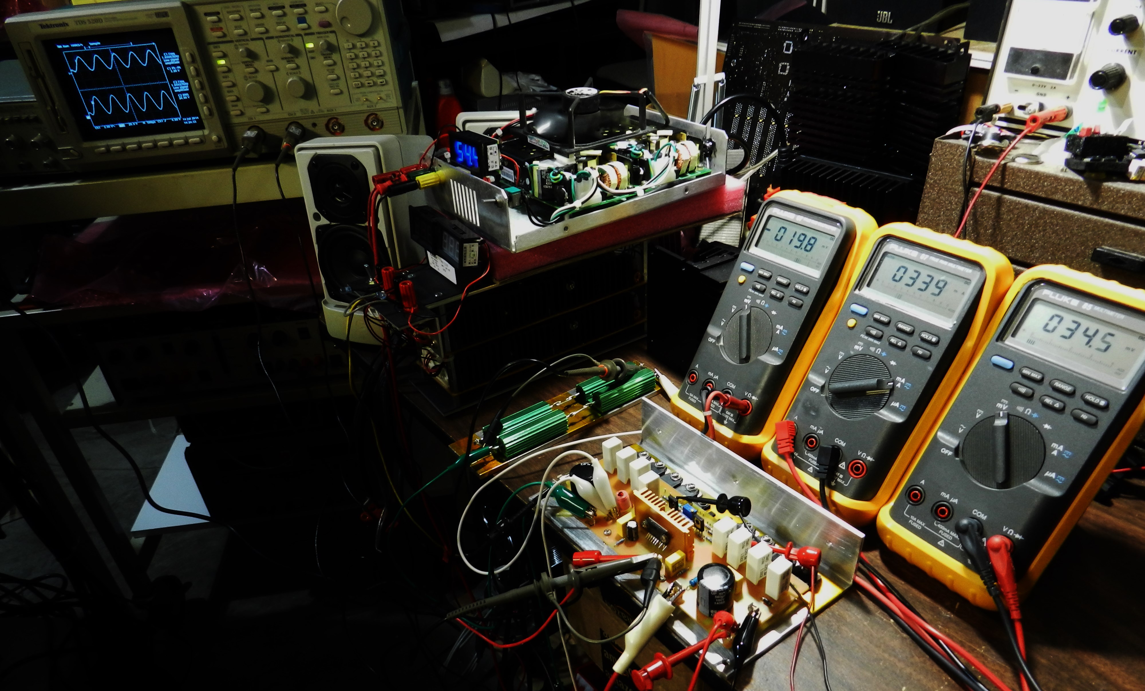

A 1KHz 4.72Vpp sine wave signal was applied to the input of the amplifier under test and produced a 33.61Vrms across the 8Ω/400W load or a power output of about 141.2Wrms before clipping occurs. Enjoy!
![]()