Project 40
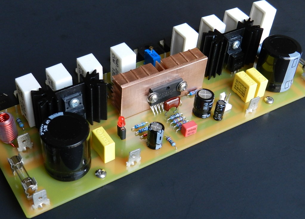
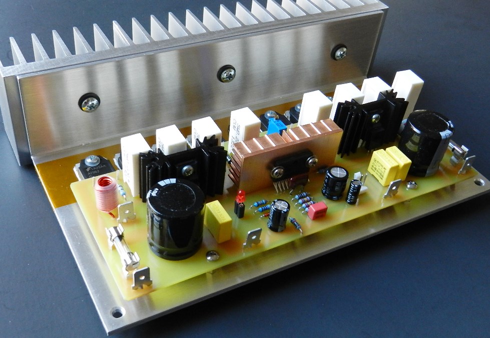
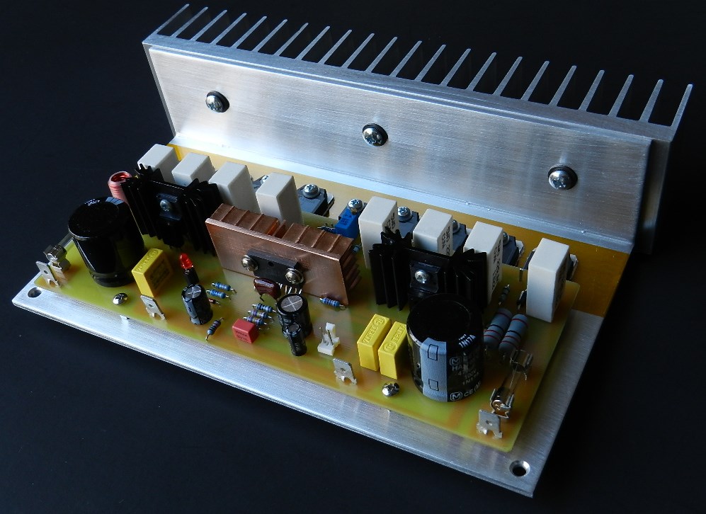
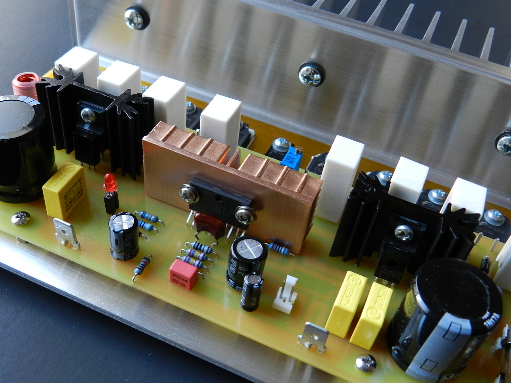
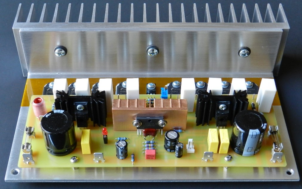
Project 40 is a scaled high-powered version of an earlier LME49810 project. The project’s power output stage is a three-stage emitter follower circuit configuration, popularly known as the Triple. The first stage is the pre-driver transistors, Q2 and Q8, which isolate the output of the LME49810 from the second stage main driver transistors, Q3 and Q9. The outputs from these driver transistors are connected to the third stage consisting of four pairs of TO3P packaged complementary power output transistors, Q4 thru Q7 for the positive side and Q10 thru Q13 for the negative side. Few changes were made to the components around the LME49810 merely for sonic improvements. Capacitor Cf placed in parallel with R3 improves high frequency response of the amplifier. The measured power output of this project is more than 220 watts at 8Ω load or more than 440 watts at 4Ω load with ±72VDC power supply rails. The voltage gain of this project is about 28.4V/V (29.1dB), determined by the value of R3 and R5. Altering their values will result in your desired voltage gain.
A unique feature of the LME49810 is the internal Baker Clamp and Clip Flag circuit. According to TI, the featured circuit insures that the amplifier power output device does not saturate when over driven. The resultant “soft clipping” of high-level audio signals suppresses undesirable audio artifacts generated when the power output transistors are driven hard into clipping. When the output at pin 1 goes into clipping, a logic low level appears at the CLPFLAG pin. The CLPFLAG pin can be used to drive an LED or other displays, and on this project a 2-pin connector, J2, was added to access the clamp circuit’s output. If you’re planning to create your PCB, keep in mind that the CLPFLAG output is an open collector it should never be left to float under normal operation. If the CLPFLAG pin is not used, then it should be connected with a 1K resistor to a 5-volt reference voltage. However, in the prototype model a small packaged red LED was installed at J2, as shown in the heading pictures. The LED will turn ON when soft clipping occurs.
Here comes the ultimate test and most exciting part of this project. The project was connected to a modified LM49720 tone control preamp. While playing “Bario Alto” and “The Mirror Conspiracy” by Thievery Corporation from their album “The Mirror Conspiracy” on a Toshiba HD-A2 player and Kenwood’s quad 12” 3-way speakers, stunning clarity on percussion, emphasis on the high frequencies, and heavy but detailed bass was experienced. The entirety of The XX’s debut album “XX” was also played using the same setup to monitor its real world performance and normal operating conditions.
If you are interested in building this project and have read the Information and Policies section of this website, the schematic diagram, PCB layout (available only by request) and BOM are free, as is, no warranty. Here’s AN8149, a power supply design from TI specifically for the LME49810, 11 and 30 modules but could also be used for any audio amplifier power supply requirements.
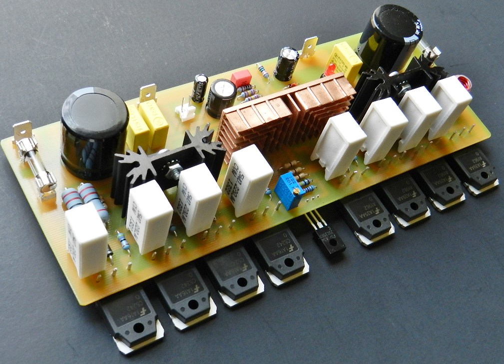
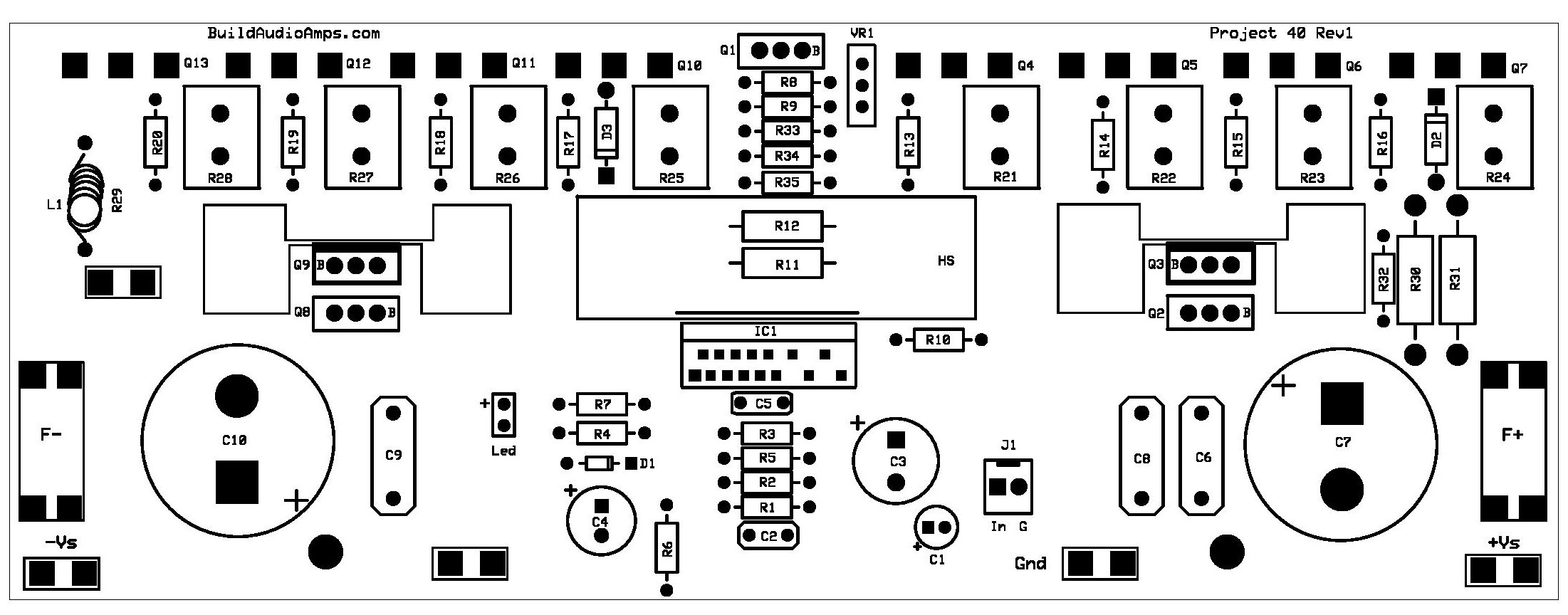 Project 40 Silkscreen Parts Placement Layer of PCB.
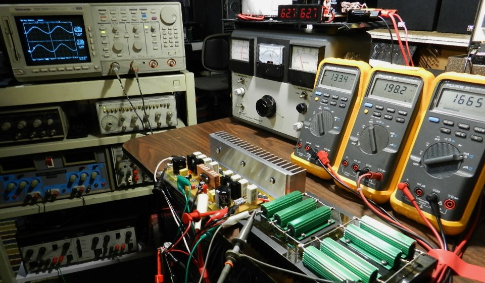
If you’ve decided to build this project, the idle current needs to be adjusted first before going any further. Insert a jumper or shunt at the input of the amplifier. Do not connect any load or loudspeaker at the output of the amplifier. Adjust VR1 for maximum resistance of 1KΩ; please refer to the schematic diagram where to access VR1 on top of PCB. Prepare 3 DMMs to measure the DC offset voltage at the output of the amplifier, the voltage between the emitters of Q7 and Q13 and the overall current across the F+ fuse terminals.
Why all the DMMs? The very first time you apply power to a newly built audio amplifier project the DMM is your very best friend. The DMMs instantly tells you if there is something wrong with your printed circuit board assembly. A very high ammeter reading indicates that a component in the circuit is drawing too much current. The same goes with a very high voltage reading at the output of the amplifier where you should expect a very low voltage reading in the millivolts range. The DMM tells you the bad news first and when the inevitable happens you immediately switch OFF the power supply and recheck the assembly. If you don't have all the DMMs connected to those important test point locations mentioned and when that tragic event happens, you only have your senses to tell you something is burning or smoke signals coming off from the populated components. The DMM also tells you the good news when everything is working just fine and that you did a good job!
It is also highly recommended to use a Variac transformer when performing the initial test of the project. If something goes wrong with the project, minimum damage will occur to the components or just a blown Variac’s fuse. However both test procedures with or without the use of a Variac transformer will be explained.
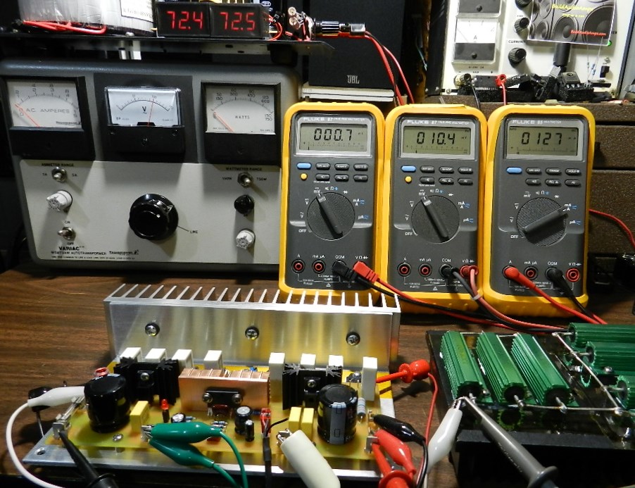
If a Variac transformer is available, connect the AC input of the power supply to the output of the Variac transformer. Switch the power to ON and gradually adjust the Variac’s AC output from zero until the voltage output of the power supply reaches approximately ±72VDC while observing for sudden increase in any DMM readings. If you have encountered an unusual increase in any of the DMM readings, switch the power to OFF immediately and check the PCB for assembly errors. The picture above shows a DC offset voltage at an amazing 0.7mV. The voltage between Q7 and Q13 is 10.4mV and could be anywhere from 8mV to 10mV; readjust VR1 to get approximately that DMM reading after a warm-up period of 10 minutes or more. From the prototype test results, it was determined that this bias voltage is the minimum actual value that produces a well-rounded peak on the output waveform. The current across the F+ fuse terminals is 127mA and could be anywhere from 100mA to 130mA; this value is dependent on the adjustment of VR1. If you obtain similar DMM readings, you may proceed with music test.
If a Variac transformer is unavailable, make sure that the power supply was properly built and that the output voltage rails have been measured approximately ±72VDC before connecting it to the amplifier project under test. With the power supply switched to OFF, adjust VR1 for maximum resistance. Switch the power supply to ON; the DMM measuring the voltage between the emitters of power transistors, Q7 and Q13, should read less than 1mV. The DMM measuring the offset voltage should read about 0.7mV. The DMM across the fuse terminals should read about 20mA or less. Other than DMM readings mentioned, power OFF immediately and check the PCB for assembly errors. When the error was corrected, adjust VR1 to get a DMM reading from 8mV to 10mV after a warm-up period of 10 minutes or more. The DMM that is connected across the F+ fuse terminals will read about 100mA to 130mA of total current. If you obtain similar DMM readings, you may proceed with music test.
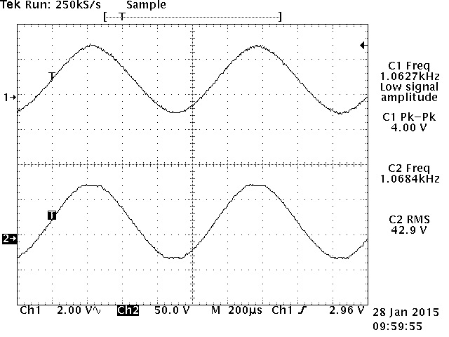
The following will show how the internal Baker clamp circuit of the LME49810 works. The encircled LED at J2, shown in the next picture, turns ON with a 4Vp-p 1KHz sine wave input peak signal. Every time the clamp circuit in the LME49810 detects this peak signal, the LED turns ON indicating, “soft clipping”. The Tek hardcopy picture shows when that event will happen, resulted in a very nice symmetrical clipping on both peaks of the output waveform, which correlates to 42.9Vrms across an 8Ω load or a soft clipped power output of 230 watts.
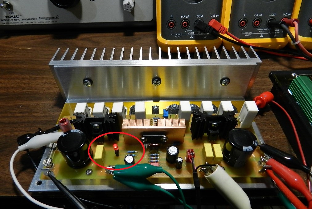
 Encircled is LED at J2, turned ON by the Baker clamp circuit. Clipped output waveform when Baker clamp circuit is enabled.
The next test procedure is optional, but if an oscilloscope, audio signal generator and 8Ω dummy load are available, the maximum power output before clipping can be measured. Be careful not to touch the project’s heatsink and dummy load, they will get very hot during this test. The power output was measured using an HP3312A Function Generator and connected directly to the input of the amplifier through a 100KΩ potentiometer wired as an attenuator, as well as the CH1 test probe of the oscilloscope. An 8Ω/700Watt dummy load was connected at the output of the amplifier under test as well as the CH2 test probe of the Tektronix TDS520D 500MHz DPO.

The prototype model of this project produces a sine wave output signal of 42.2Vrms across the 8Ω/700W dummy load or a power output of more than 220watts with an applied input sine wave signal of 3.76Vp-p. The oscilloscope’s horizontal scale was adjusted at 200uS to verify for any visible clipping or artifacts on either peak. This project was paired with a passively modified PreAmp1 tone control project; the audio quality it reproduced was excellent.