Project 52
Project 52 is another CFA-based audio power amplifier project. The input stage is similar to an earlier CFA-based project, but the output stage utilizes power MOSFETs arranged in a quasi-complementary configuration.
Why use power MOSFETs? Power MOSFETs have excellent performance compared to bipolar transistors, mainly because they have positive temperature coefficient of resistance. The positive temperature coefficient of resistance means that it is essentially more stable with temperature fluctuation and protection against thermal runaway and secondary breakdown. Another benefit of this characteristic is that MOSFETs can be operated in parallel without fear that one device will deprive current from the others. If any device begins to overheat, its resistance will increase, and its current will be directed away to cooler devices. Basically, that’s exactly what’s implemented in this project -paralleled N-channel MOSFETs. To understand more about MOSFETs here’s AN-7500 from Fairchild Semiconductor.
Although this project utilizes newer power MOSFETs instead of BJT devices, this topology came into existence in the 1960’s. During that time, there was no choice but to use quasi-complementary output stage design because of the unavailability of complementary high power transistors. This type of topology might not be acceptable to some builders for home use, but it certainly deserves to be an alternative option for high power live sound reinforcement applications. In 1967 Crown introduced their first solid-state high-powered stereo amplifier, the DC300A. The rated power of this amplifier at clipping point is 190 watts into 8Ω with a mere slew rate of 8 volts per uS. It employs a 1KW power transformer with large computer-grade filter capacitors capable of high-energy storage that provides power to a quasi-complementary configured eight 2N3773 power output NPN transistors per channel. Then in the late 90’s, Adcom introduced their high-current MOSFET stereo power amplifier utilizing sixteen IRF244 per channel also arranged in a quasi-complementary configuration.
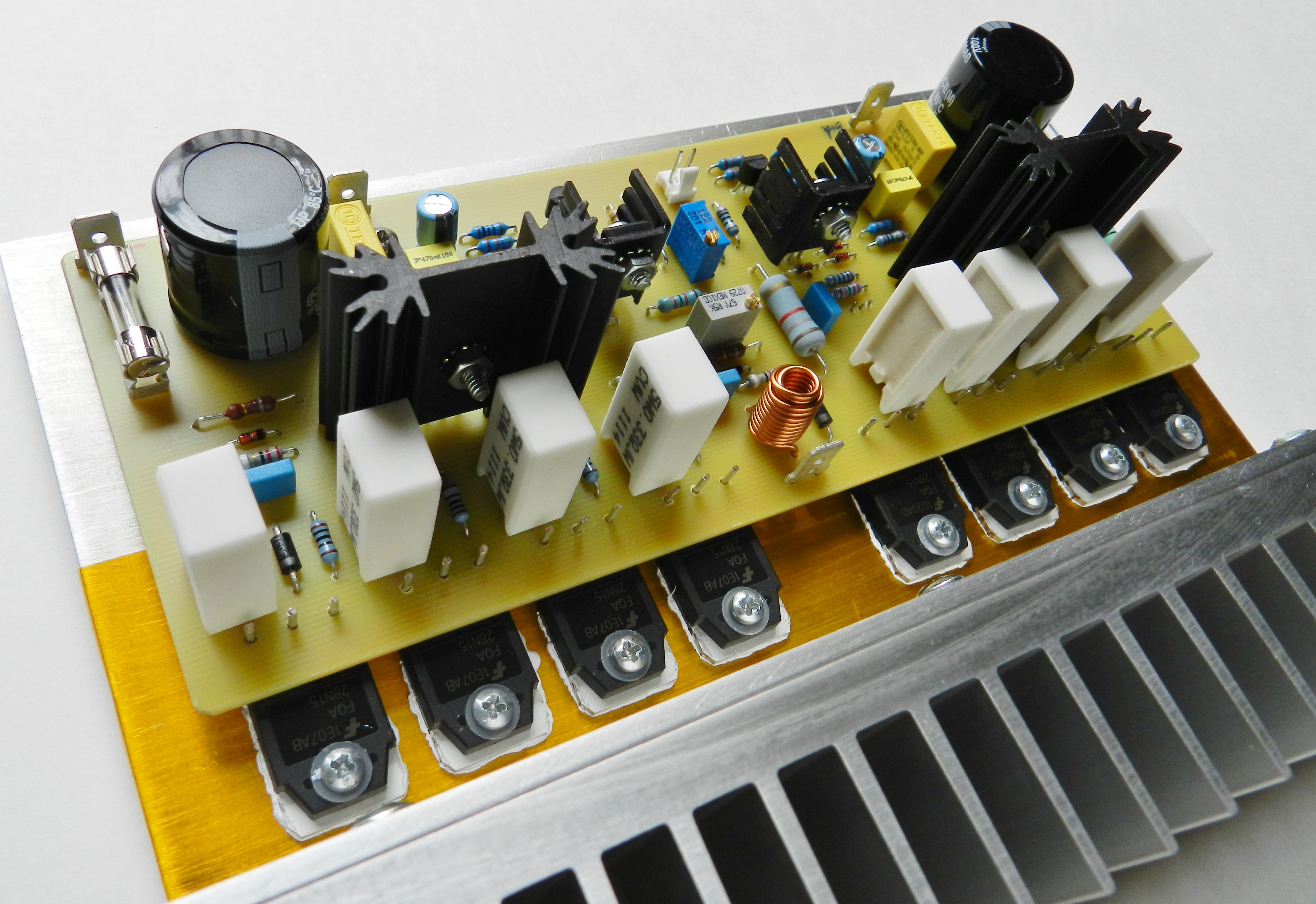
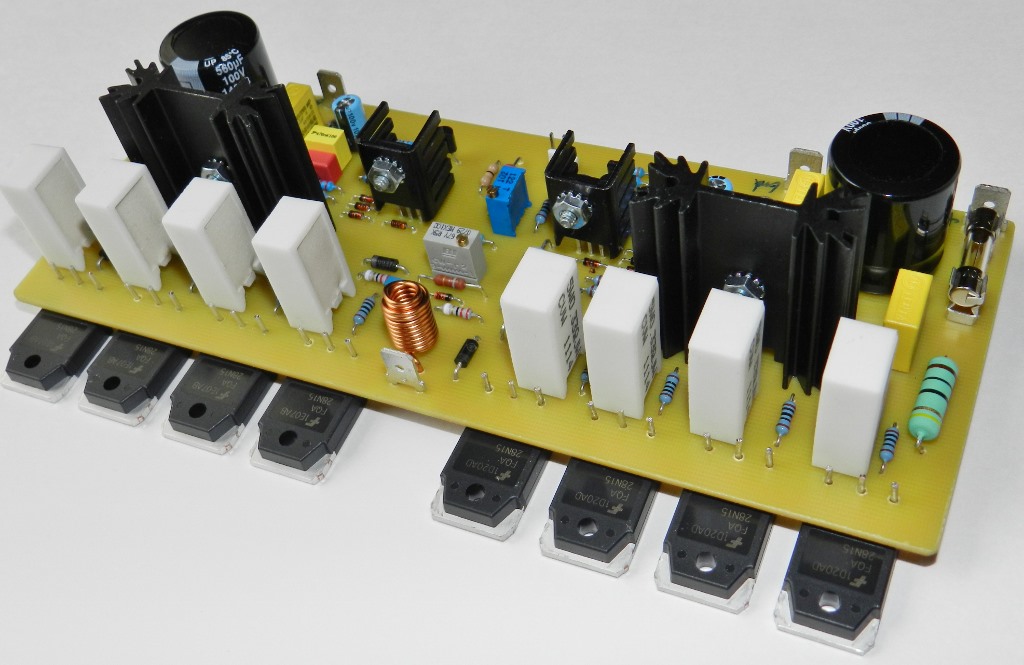
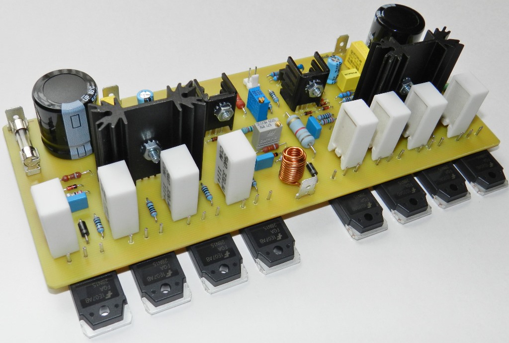
The prototype was populated with eight N-Channel QFET power MOSFETs from Fairchild Semiconductor, to amplify the upper and lower halves of the input signal. A pair of complementary 50-watt TO220-packaged MOSFET drivers effectively drives the power output stage MOSFETs. Interestingly, the prototype was also successfully evaluated with HEXFET power MOSFETs. Most quasi-complementary MOSFET circuits out there are driven by BJT drivers but not in this project. However, a high-powered BJT driven quasi-complementary N-channel power MOSFETs project is in the works! The addition of a Baxandall diode at the P-channel MOSFET driver provides improvement in its distortion characteristic and it gets as good as any complementary symmetrical source-follower design. Moreover, the implementation of a CFA-based input stage improved the overall sonic performance of this project.
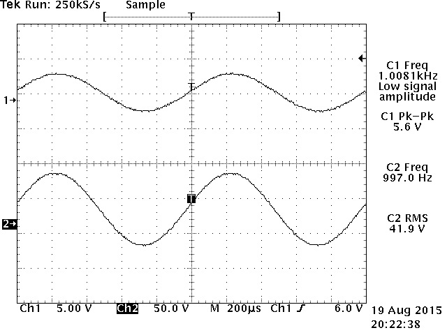
The prototype achieved a 41.9Vrms across an 8Ω load with a ±64VDC power supply rails. The actual power output test result will be shown later, as well as Noise, THD, THD+N, SNR and frequency response measurements. Actual square wave slew rate measurements at 25KHz and 100KHz are shown in the next Tek hardcopy pictures. The square wave input signals were adjusted just before showing any signs of overshoot at either positive or negative peaks of the output waveform.

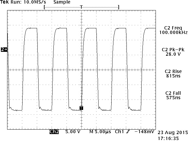
25KHz square wave test result. 100KHz square wave test result.
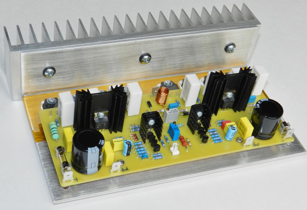
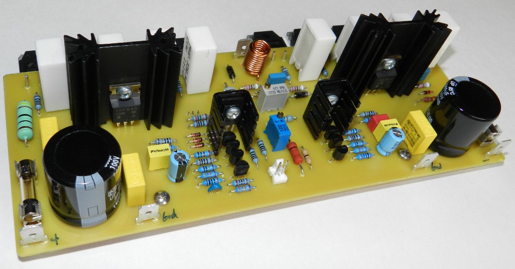
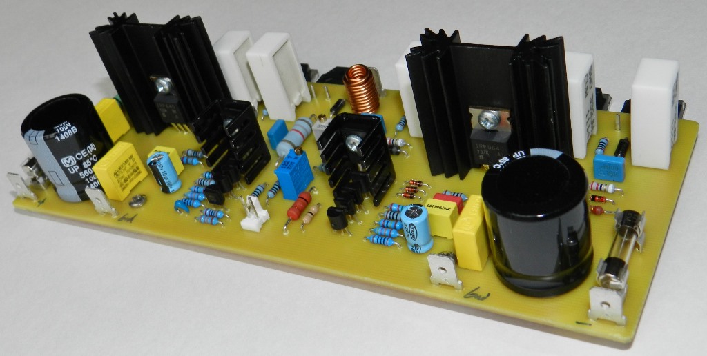
The prototype model was built on a 7.397” X 3.0” single-sided PCB. All components used in the prototype model are readily available standard parts. If you are interested in building this project and have read the Information and Policies section of this website, the schematic diagram, PCB layout and BOM (available only by request) are free, as is, no warranty.
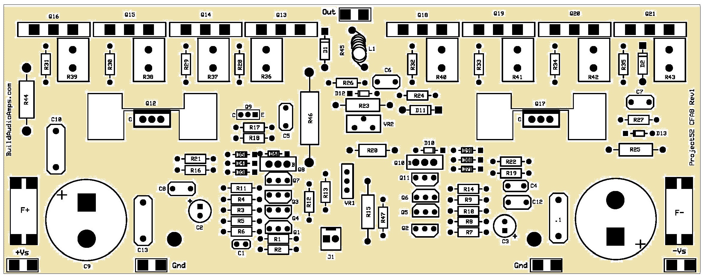 Project 52 Silkscreen top layer of PCB.
Initial tests. Before mounting the power MOSFETs into the heatsink, apply a generous amount of heatsink compound to the drain metal thermal pad of these transistors. After securing them into the heatsink, measure for a very high resistance ohmmeter reading (∞) between drain of all power MOSFETs and heatsink. The completed prototype pictures can be seen at the bottom of this page.
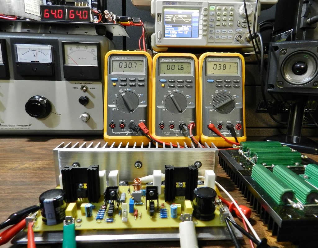
The amplifier requires approximately ±64VDC power supply rails, produced from a rectified and filtered 90VCT at 300VA power transformer or higher. The picture below shows a digital panel voltmeter reading at approximately ±64VDC, obtained by connecting the AC input of the power supply to the AC output of a Variac transformer. Gradually adjust the Variac transformer so that the digital panel voltmeter reads from 0V to about ±64VDC while observing the DMMs: connected at the output of the amplifier, across any of the source resistors R36 through R43 and the overall current at F+ fuse terminals. Power off immediately if you have noticed higher DMM reading other than what’s shown in the picture. Check the PCB for any possible assembly errors before powering up the amplifier again.
Reapply power after the fault was determined and corrected. Allow the amplifier under test to warm up for more than 15 minutes before making any adjustments to VR1 and VR2. As shown in the picture below, the DMM on the left side of the picture measures 30.7mV across any source resistors, R36 through R43; this is set by VR2 and it could be anywhere from 15mV to 33mV depending on the builder. The DMM in the middle is measuring the DC offset voltage at 1.6mVDC, which can be set by VR1 and this could be adjusted as close to 0mV as possible. The DMM on the right side of the picture is measuring the overall current across the F+ fuse terminals at 381mA and is dependent on the setting of VR2.
Optional tests. The next picture below shows the test setup for power output and slew rate measurements. During this test, be careful not to touch the amplifier’s heatsink and dummy load; they will get very hot! An SDG805 function/arbitrary waveform generator and a Tektronix TDS520D 500MHz oscilloscope were used for these particular tests. However, any similar test equipments may be used if you’re planning to perform the same optional tests. The dummy load is only connected to the amplifier during power output measurement. It should be disconnected from the output of the amplifier during slew rate measurement. The Zobel network resistor R44, a 10Ω 3W wire wound power resistor, should be disconnected as well. Running a continuous high frequency square wave signal to the amplifier will damage this resistor.
The measured power output of the amplifier just before clipping is about 219 watts at 8Ω with ±64VDC power supply rails. This power output was achieved by applying a 1KHz at 5.6 Vp-p sine wave input signal to the amplifier that produces before clipping 41.9 Vrms across the 8Ω dummy load. The Tek hardcopy picture of the power output test result is shown below on the right. Shown earlier are Tek hardcopy pictures of the slew rate measurement output waveforms. These were obtained by applying a 25KHz and 100KHz square wave signal to the input of the amplifier and was adjusted so that the output waveform does not show any overshoots on its peaks at approximately 28Vp-p.
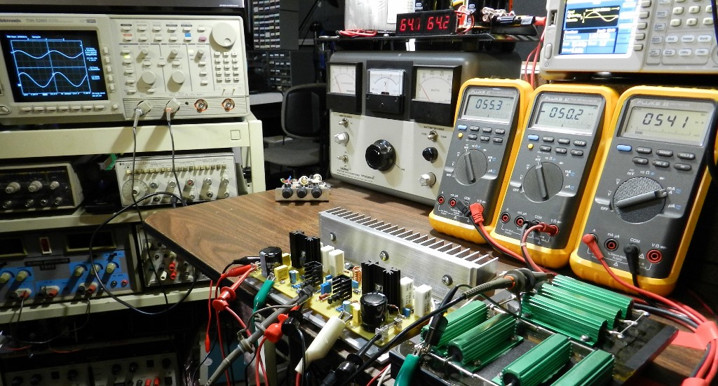
Audio analyzer tests. The picture below shows an 8Ω dummy load, Project 52, QA190, QA400, DMMs, Variac/power supply and a Dell laptop computer. This is a simple test setup in performing some basic audio measurements to the power amplifier project with acceptable results. A QA400 24-bit Real Time Audio Analyzer from QuantAsylum was utilized to measure noise, THD, THD+N, SNR and frequency response. The QA400 is USB powered, controlled by its own application software and can generate and analyze very accurately a series of burst test tones. For this test, the USB hardware was connected to a Dell laptop computer that’s running a Windows 7 operating system.

The input clipping level on the QA400 is +3dBV or 4Vpp. As it is, it’s good enough for testing low voltage level preamplifier or tone control projects. It is however a problem when testing power amplifiers that’s producing very large amount of voltage. To avoid this damaging condition to the QA400, it is necessary to attenuate the high voltage signal coming from the output of the power amplifier project. To do that, a QA190 Low Noise Differential Probe must be connected to the input of the QA400. The QA190 clamps the high-voltage signal from the output of the amplifier under test to safe level of about ±4 volts. The QA190 is also fitted with a /10 and /100 range switch for convenience.
The next pictures below will show the captured QA400 display area test results of Project 52. These test results were acquired by connecting the input test clips of the QA190 to the 8Ω dummy load. This dummy load is also connected at the output of the amplifier under test. The range switch of the QA190 is set at /100. The output of the QA190 is then connected to the left channel input of the QA400. The left channel output of the signal generator of QA400 is directly connected to the input of the amplifier under test. A USB able is connected to the laptop or desktop computer, which powers and sends data to the QA400.
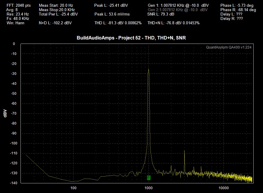
Project 52 QA400 Noise, THD, THD+N and SNR test result.
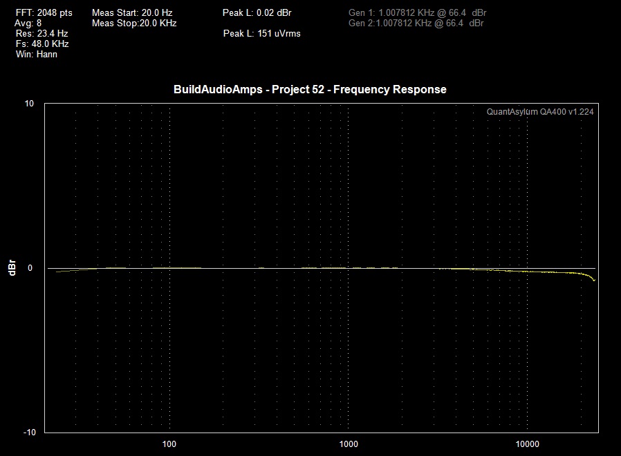
Project 52 QA400 Frequency Response test result.
How does Project 52 sound? In real world listening it did not disappoint but was very impressive and powerful, in spite of the quasi-complementary topology. The prototype unit was connected to a modified LM49720 tone control preamp, a Toshiba HD-A2 player and quite a few sets of test speakers. Several CDs of diverse music genres were auditioned to conscientiously listen and categorize which particular type of music does this project would prefer, but it did not!