Project 59

The Low TIM Amplifier, also popularly known as The Leach Amplifier, was designed by W. Marshall Leach Jr. and inspired Project 59. The LeachAmp has been successfully built or modified by many audio electronics do-it-yourselfers since the early ‘90s. Project 59 is comparable to the Erno Borbely-inspired Project 34 and Project 31 that use a complementary-symmetrical differential input stage circuit. The input stage topology was also used by G. R. Slone in his quest for the optimum audio power amplifier design and appropriately named it as the mirror-imaged input stage topology. Worth mentioning is a comparable project – the penultimate fully mirror-imaged Project 44.
You can read the entirety of “The Leach Amplifier” original design plans at http://users.ece.gatech.edu/mleach/lowtim/. However, prior to the Leach Amplifier project, he published an earlier article about his unique audio power amplifier design in the Audio Magazine February 1976 issue entitled, "Build a Low TIM Amplifier". The Low TIM Amplifier design went through four phases of revisions, the Low TIM 4 being the last, published on May 1986. The amplifier when connected to an 8Ω load has a power rating of about 100 to 120 watts depending on the power supply from ±52VDC to ±59VDC rails. The amplifier is a direct-coupled complementary symmetrical differential input stage topology. The last version of the Low TIM amplifier features a very interesting negative feedback scheme, which he called the feedforward frequency compensation network. The feedback network was added at the emitter resistors of the pre-driver transistors to the bases of the differential error amplifier transistors.
The core design of the Low TIM 4 Amp will be the basis of Project 59, however, all active components were replaced with readily available parts. The values of some of the passive components, especially in the output stage circuit, were changed to meet with the planned higher power supply voltage rails. The original schematic diagram of The LeachAmp was redrawn for simplicity so that other stages that have been intentionally removed, particularly the protection circuits in the output stage, are not shown. The modified schematic diagram will be the primary basis of creating the PCB layout of Project 59 and will be referred to from hereon.
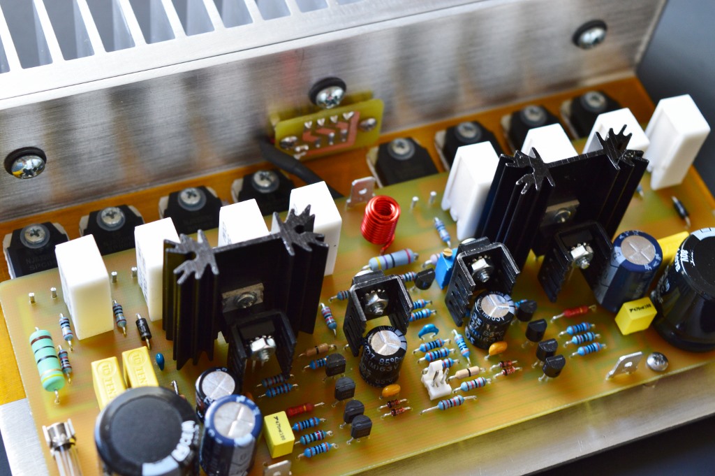
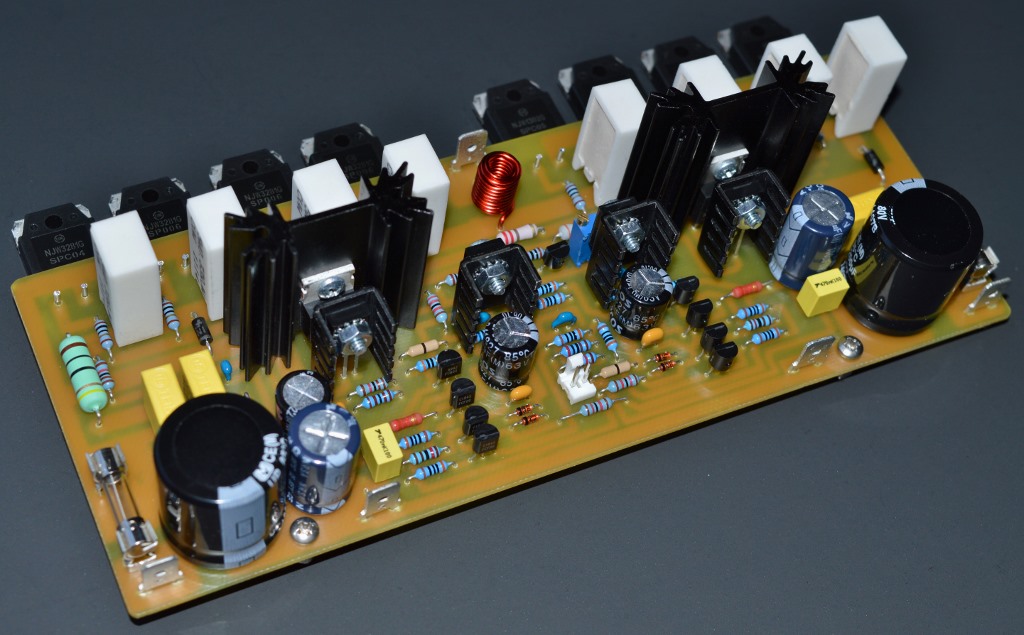
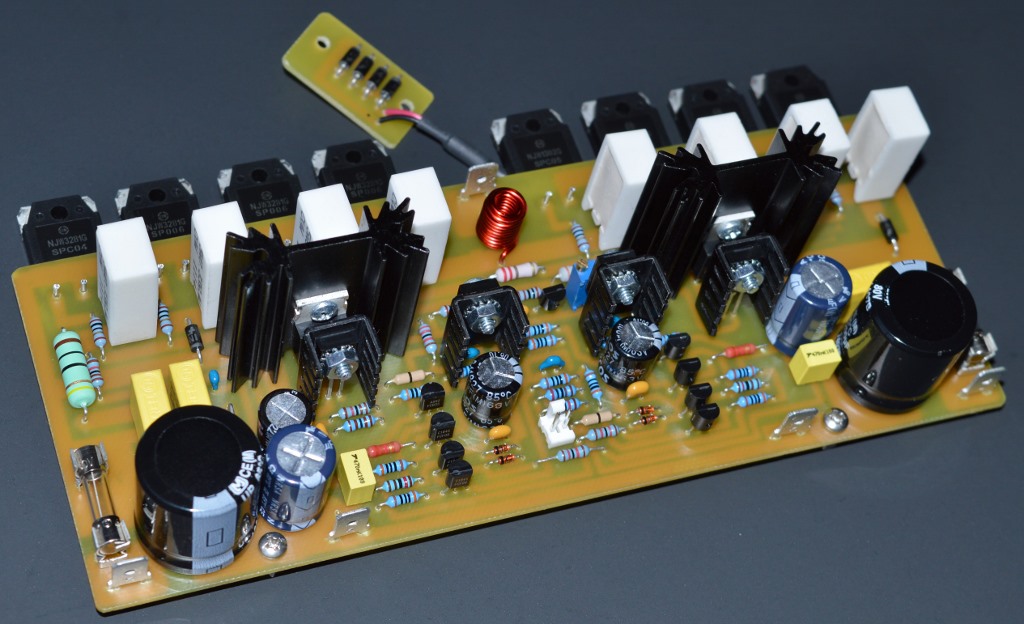
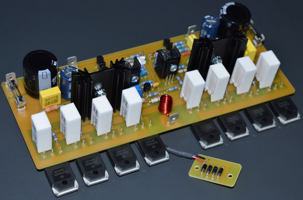
The prototype’s layout was created using ExpressPCB software, laser printed and etched into a 7.75” X 3” single-sided printed circuit board. The header pictures on top of the page show the initial build at Rev1, while the completed prototype shown at the bottom is at Rev2. Notice the difference in the resistance values of the emitter resistors, R29, R30 and R31. The PCB layout and BOM are free to registered users only and available only by request, as is, no warranty.
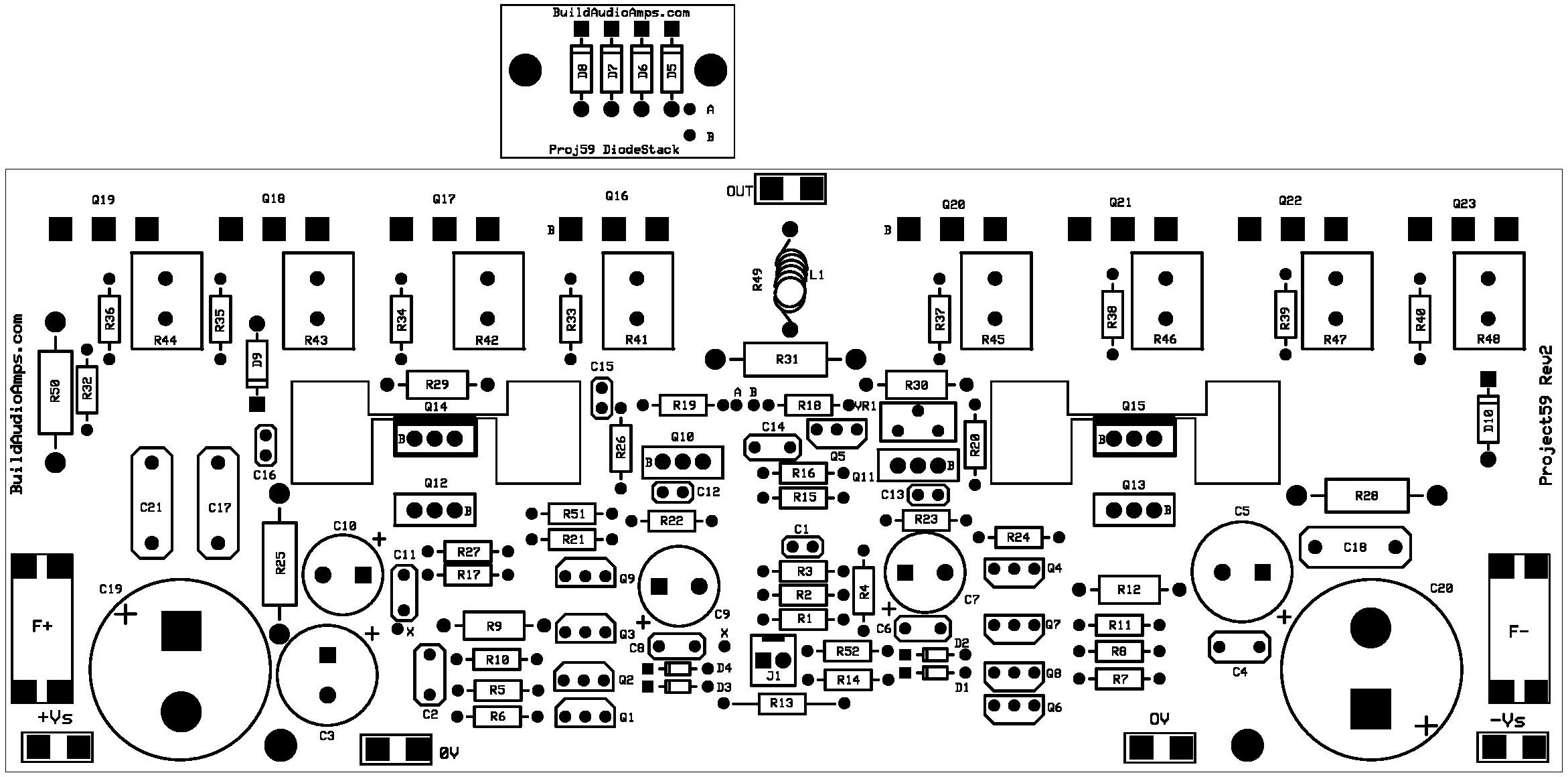
Project 59 Parts placement top layer of PCB.
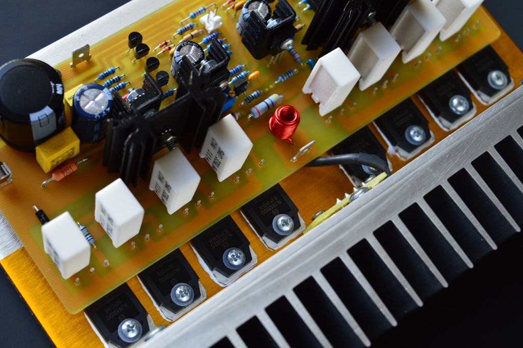
The prototype requires ±64VDC power supply rails, obtained from a rectified and filtered 45VAC-0-45VAC 300VA or higher power transformer. The increase in the power supply voltage rails requirement would result in a higher power output especially when connected to low impedance loads. Four pairs of NJW3281/NJW1302 power transistors were chosen for the power output stage to increase its power dissipation capability. The pre-driver as well as the driver transistors were also replaced with higher rated devices. The complementary pair driver transistors are rated at 250V 17A and can dissipate a power of about 80 watts. During listening test these heat-sinked driver transistors never increased their package temperature to more than 62°C.
The bias current in the pre-driver and driver transistors was increased; this is necessary for the paralleled power output stage devices. Decreasing the original values of the emitter resistors R29, R30 and R31 increases the bias current. The adjusted values produce 11mA for the pre-driver transistors, Q12 and Q13, and 24mA for the driver transistors, Q14 and Q15. The change also decreases the DC offset voltage of the amplifier to almost 0mV, which will be shown later during the initial test and noticeably improved the audio quality of the amplifier.
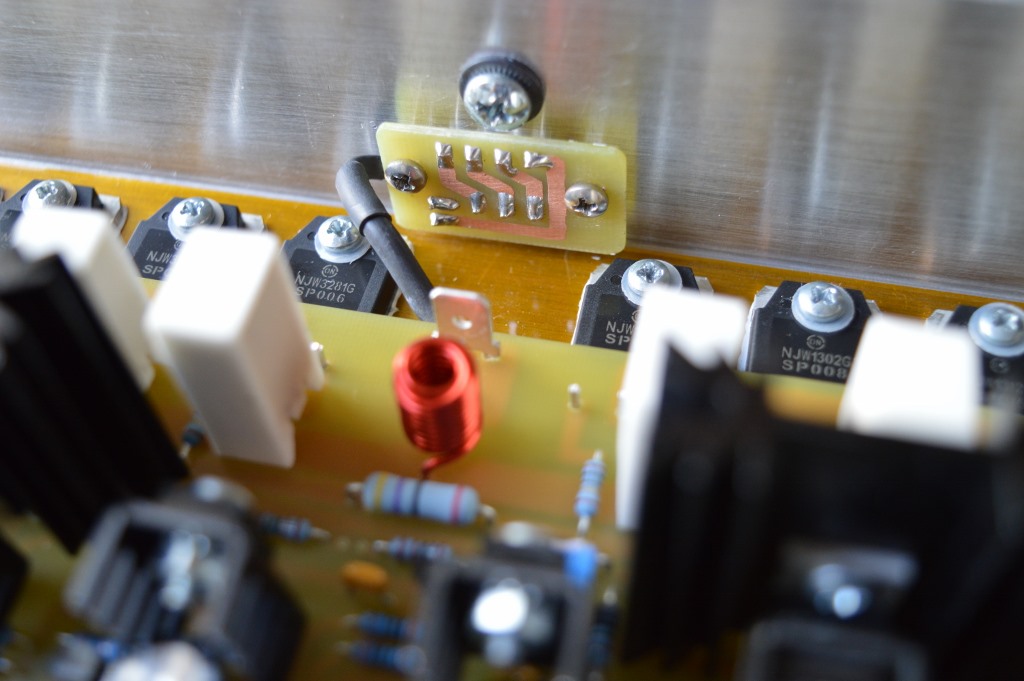
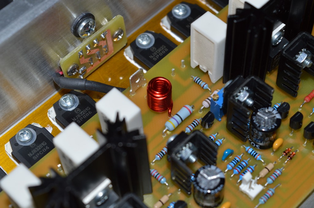
The original value of R25 and R28 were changed so that the input stage circuit can be safely connected to the planned higher power supply rails. Another method is to increase the value of R9 and R12 to 5.6K 1W, as implemented in the Leach SuperAmp, also known as the double-barreled amplifier. The diode stack, D5 through D8, in the VBE circuit is now populated into a small PCB and can then be easily mounted in the middle of the power output transistors. The current gain (hFE) of the small signal transistors, Q1~4 and Q6~9, were all matched at about 450 using a cheap DMM with built-in hFE range. This was suggested in the LeachAmp plan and proven to be an effective assembly step as shown in the test result.
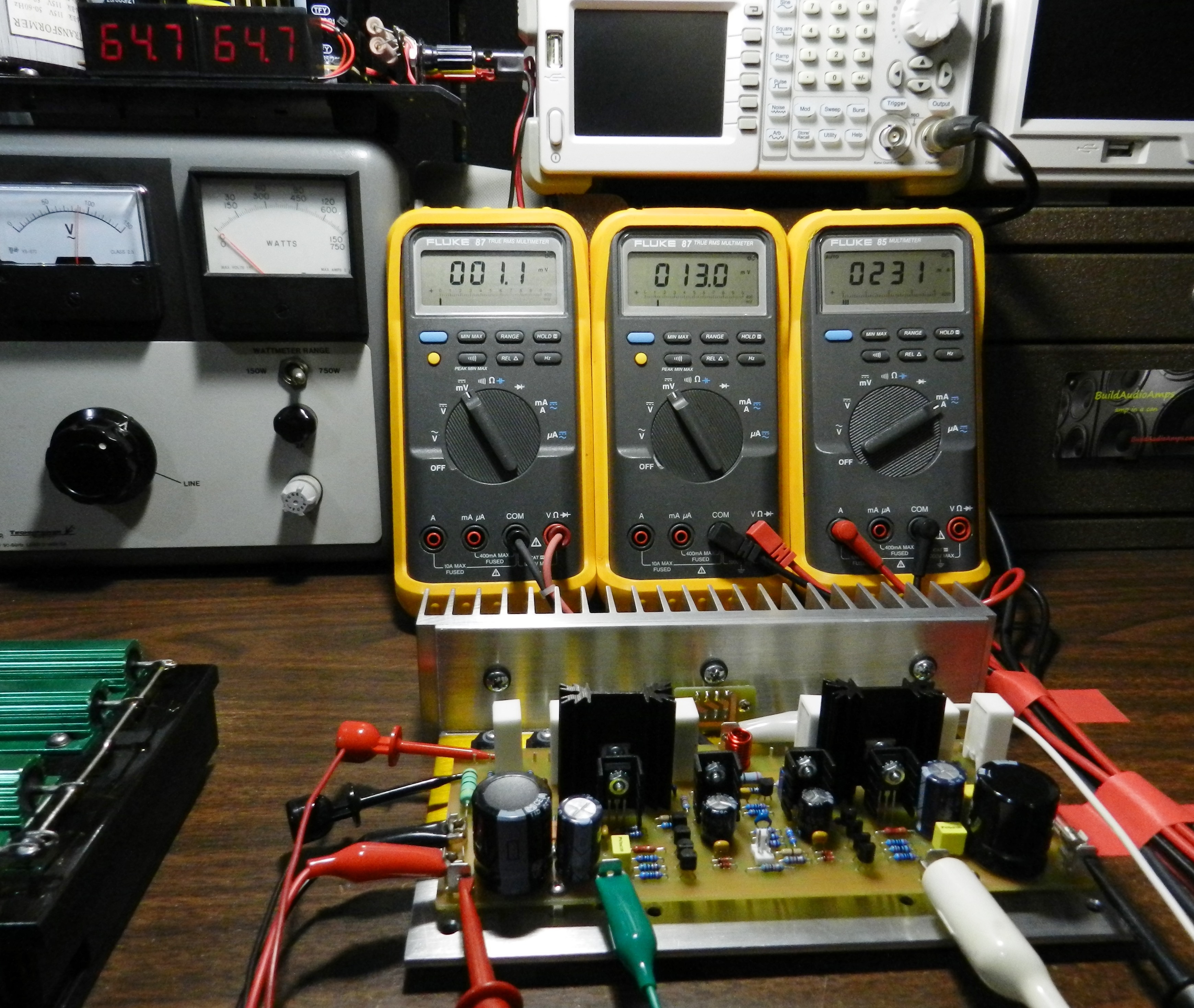
The picture shown above is the initial test setup and DMM readings of Project 59’s prototype. Also shown in the picture are two digital panel voltmeters that are connected at the output of the test power supply DC voltage rails. Before applying power to the amplifier, VR1 must be adjusted to maximum resistance (2KΩ). You may adjust VR1 only after a warm-up period of more than 15 minutes to set the required bias. If you plan to build this project, assuming an error-free PCB assembly, you should have the same DMM readings as shown in the above picture.
The DMM on the left is connected to the output of the amplifier; this measures the output DC offset voltage of the amplifier at 1.1mV, because of hFE matching. The DMM in the middle is connected across R44 (red and black test clips, can be seen on the left side of PCB); this measures the voltage drop across the emitter resistor of Q19 at 13mV. The voltage drop of 13mV divided by the resistance value of the emitter resistor at 0.33Ω is equal to the bias current of Q19/Q23 transistor pair at about 40mA. The same 13mV reading should be approximately present across R41, R42 and R43. The DMM on the right is connected at the F+ fuse terminals (red and black test clips as seen on the left side of the PCB); this measures the total current drawn by the amplifier at about 231mA and is dependent on the adjustment of VR1.
Another method of testing the amplifier after assembly is found in the LeachAmp Construction and Test section. You may proceed to the listening test if you have obtained the same DMM readings, as explained in the preceding test procedure; otherwise, you may perform the next optional power output, square wave response and QA400 tests.
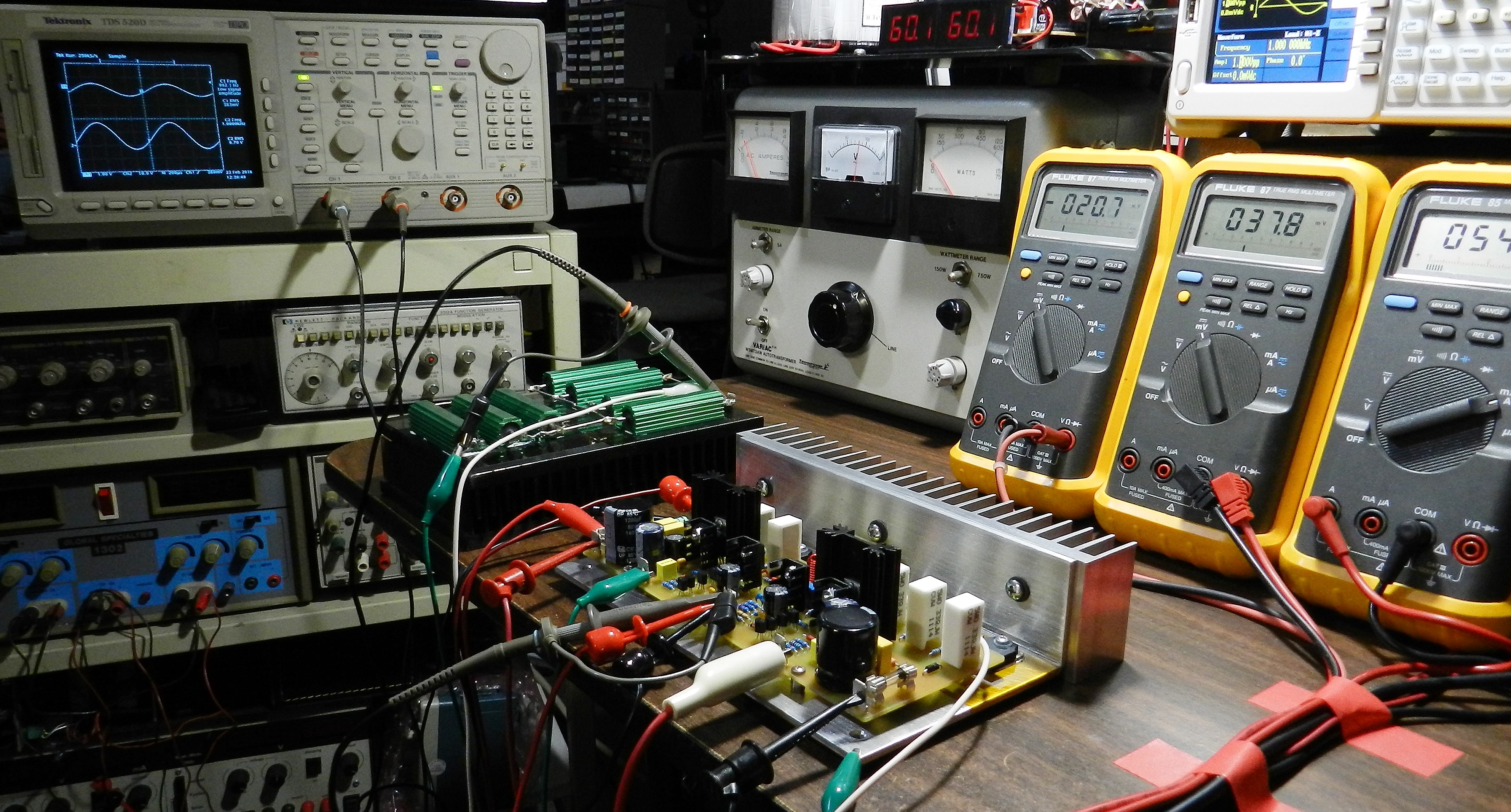
The picture above shows the test setup for power output measurement and square wave response test. The prototype was able to amplify the 1KHz 1.96Vrms sine wave input signal to 40.9Vrms across an 8Ω dummy load. This corresponds to an unclipped power output of 209 watts. At about 1Vrms of the same input signal, the prototype produces a power output of 35.91 watts. The actual power measurements are hardcopied by a Tektronix TDS520D digital phosphor oscilloscope and shown in the next pictures. An SDG805 function/arbitrary waveform generator was utilized to generate the necessary input signals to the amplifier under test.
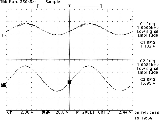
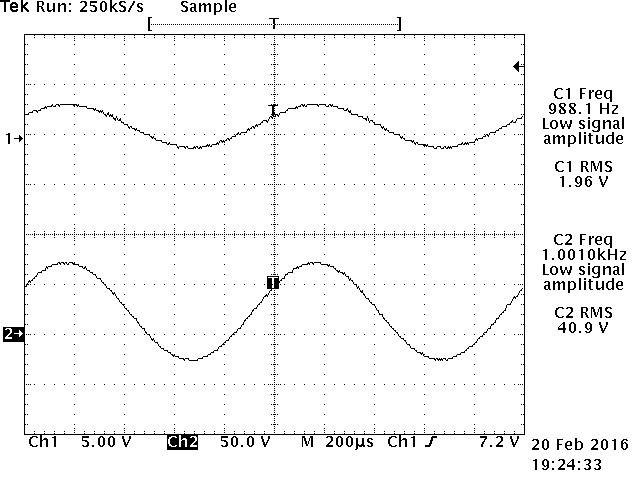
1Vrms input signal produces a power output of 35.91 watts. 1.96Vrms input signal produces a power output of 209.1 watts.
The following Tek hardcopy pictures will show the 20KHz and 100KHz square wave response test results. The amplitude of both 20KHz and 100KHz square wave signals were adjusted just before displaying any sign of overshoots on either peaks of the waveforms. At 20KHz square wave the amplifier produces 112Vp-p with a rise time of 834nS and a fall time of 795nS. Then at 100KHz square wave signal it produces 104Vp-p with a rise time of 739nS and a fall time of 728nS. If you’ll perform this test, be sure to remove R50 from the circuit. Continuously running a high frequency square wave input signal into the amplifier and adjusted at high amplitude level will absolutely damage this resistor.
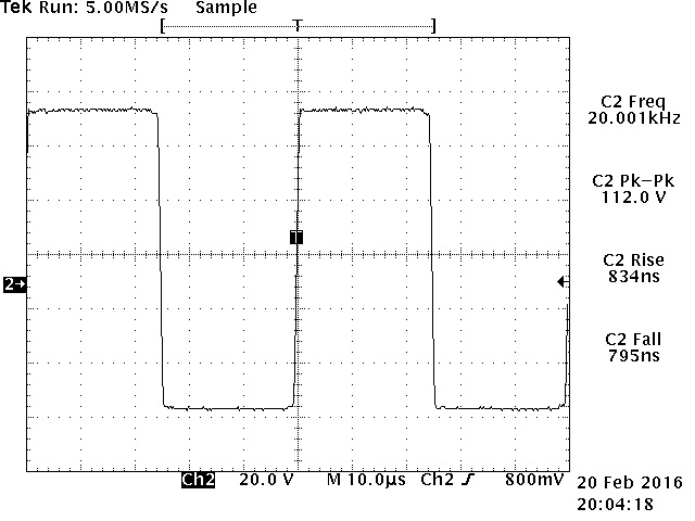
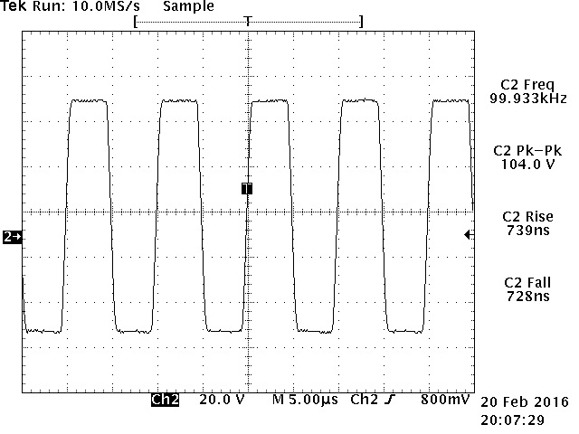
20KHz square wave response test result. 100KHz square wave response test result.
The next Tek hardcopy pictures will show the effect of altering capacitors, C15, C12 and C13. These are the key components that will determine how good the square wave frequency response is and ultimately the slew rate. The Tek hardcopy picture on the left below shows the 100KHz square wave frequency response if C15 was removed. The picture on the right below is the 100KHz square wave frequency response if C12 and C13 were both increased to 100pF.

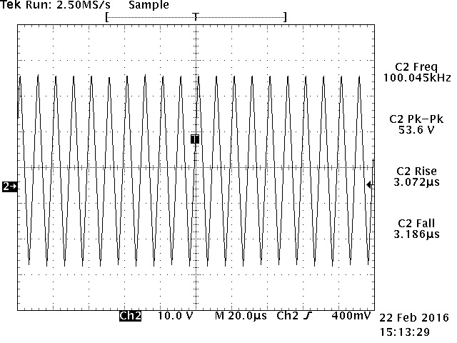
Square wave response if C15 is removed from the circuit. Square wave response if C12 and C13 are 100pF.
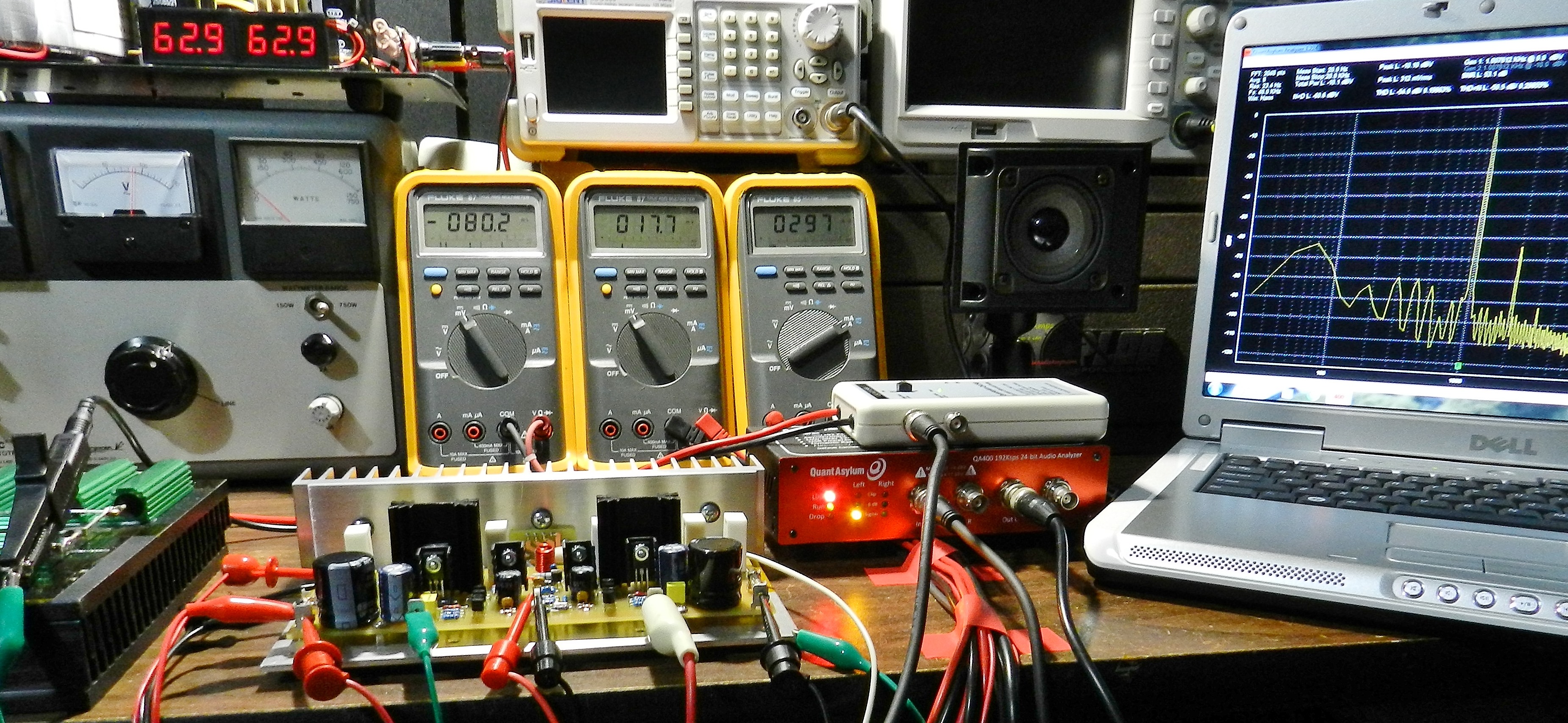
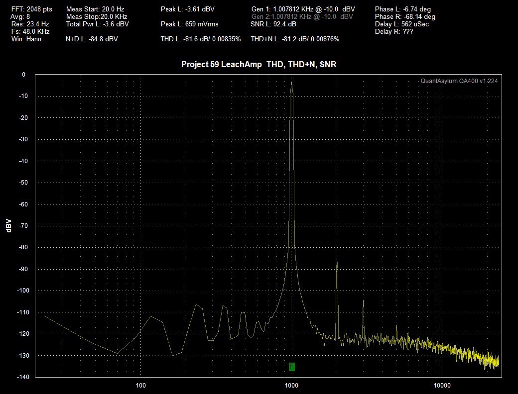
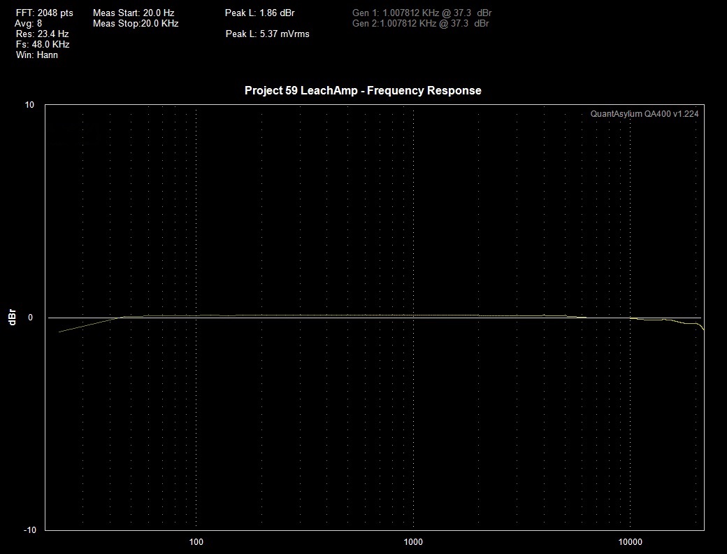
The picture above shows an 8Ω dummy load, Variac/power supply, Project 59, DMMs, QA190, QA400 and a laptop computer. This is a simple test setup in performing basic audio measurements to Project 59’s prototype with very good results. A QA400 24-bit Real Time Audio Analyzer from QuantAsylum was utilized to measure noise, THD, THD+N, SNR and frequency response. The QA400 is USB powered, controlled by its own application software and can generate and analyze very accurately a series of burst test tones. For this test, the USB hardware was connected to a battery-powered laptop computer that’s running the Windows 7 operating system.
The input clipping level on the QA400 is +3dBV or 4Vpp. As it is, that’s good enough for testing low-voltage level preamplifier or tone control projects. It is however a problem when testing a power amplifier that’s producing a very large amount of output voltage. To avoid this damaging condition to the QA400, it is necessary to attenuate the high voltage signal coming from the output of the power amplifier project. One of several ways is to connect a QA190 Low Noise Differential Probe to the input of the QA400. The QA190 clamps the high-voltage signal to a safe level of about ±4 volts. The QA190 is battery powered and is also fitted with a selectable /10 and /100 range switch for convenience.
The left or right channel signal generator output of the QA400 is directly connected to the input of the amplifier under test. Depending on the type of measurement, the signal generator generally generates a 1KHz sine wave signal at -10dB with a sweep span from a start frequency of 20Hz to a stop frequency of 20KHz; however, all these values are user definable. Although, QuantAsylum have released their second generation of audio analyzer, the QA400 will suffice at this time to show the measured performance of the built audio amplifier project.
The next captured QA400 display area pictures will show the test results of Project 59.
How does Project 59 sound? The prototype unit was connected to a modified LM49720 tone control preamp, a Toshiba HD-A2 player and quite a few sets of test speakers. Listening to Legacy Audio’s Music Sampler Volume 3, particularly tracks 2, 5 and 10 you hear natural-sounding bass, mids and highs. It’s totally dead silent between tracks with the volume control adjusted at 50 percent. Several CDs of diverse music genres were also played that resulted to an enjoyable listening experience as well.