Project 7
Here's a brief description of the circuit:
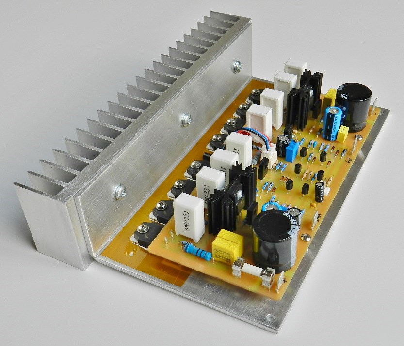
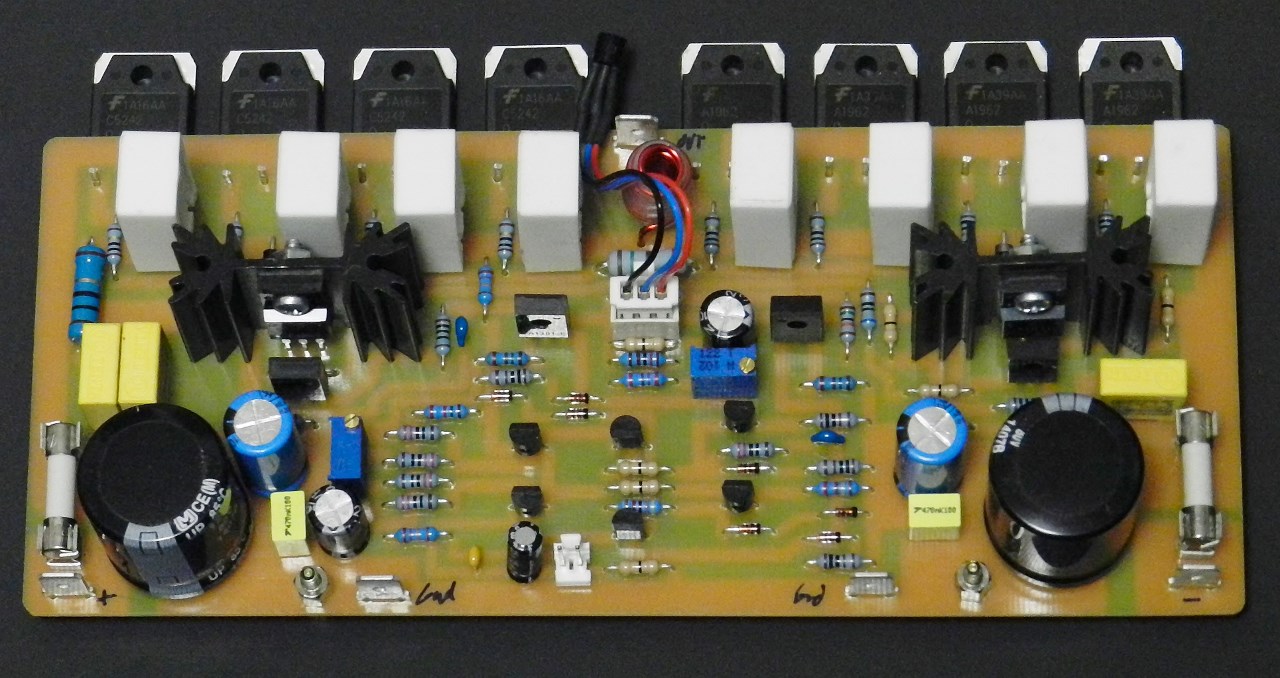
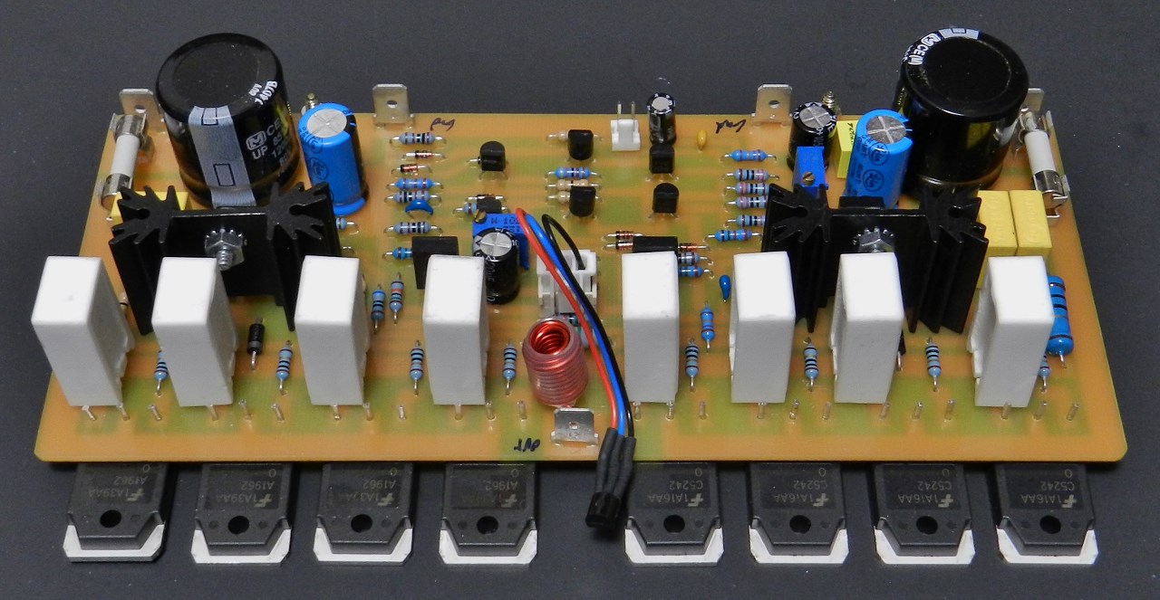
Project 7 uses 4 pairs of 2SC5242/2SA1962 complementary power output transistors.The input stage is a differential amplifier circuit consisting of Q1/Q2, current-sourced by Q3, D1 and D2. The output DC offset voltage can be manually adjusted to minimum by VR1. The collectors of Q1 and Q2 are connected to the emitters of Q4 and Q5. This type of circuit improves the bandwidth and the high frequency response of the amplifier. The outputs of Q4 and Q5 are connected to the voltage amplifier stage Q6 and Q8 loaded with a current source circuit Q7/D7. Q10 to Q13 are complementary drivers that isolates the VAS from the power output stage transistors Q14 to Q21. The driver transistors are emitter-followers configured similar to a T-circuit topology. The emitters are connected together by their resistors not tied to the output of the amplifier.
The gain of the amplifier is determined by the ratio of R8 and R7 in series with C5. VR2 adjusts the idle current of power output stage and that Q9 hopefully maintains that setting. Q9 is populated off the PCB so that it can be attached to the aluminum bracket or in any of the power transistors. L1, R44 and C12 are necessary for stability of the amplifier at any loads. Go to How-to section to see how L1 is made. The schematic diagram does not show any resistor in parallel with L1, you can use a 4.7 Ω 2 watts SMT-type resistor populated at the bottom copper layer side of the PCB. The project is able to deliver a power output of more than 100Watts rms into an 8Ω load using a power supply of ±56VDC.
If you plan to build this project, a PCB layout, Bill Of Materials Project7 BOM and schematic diagram are provided free by request, as is, no warranty.
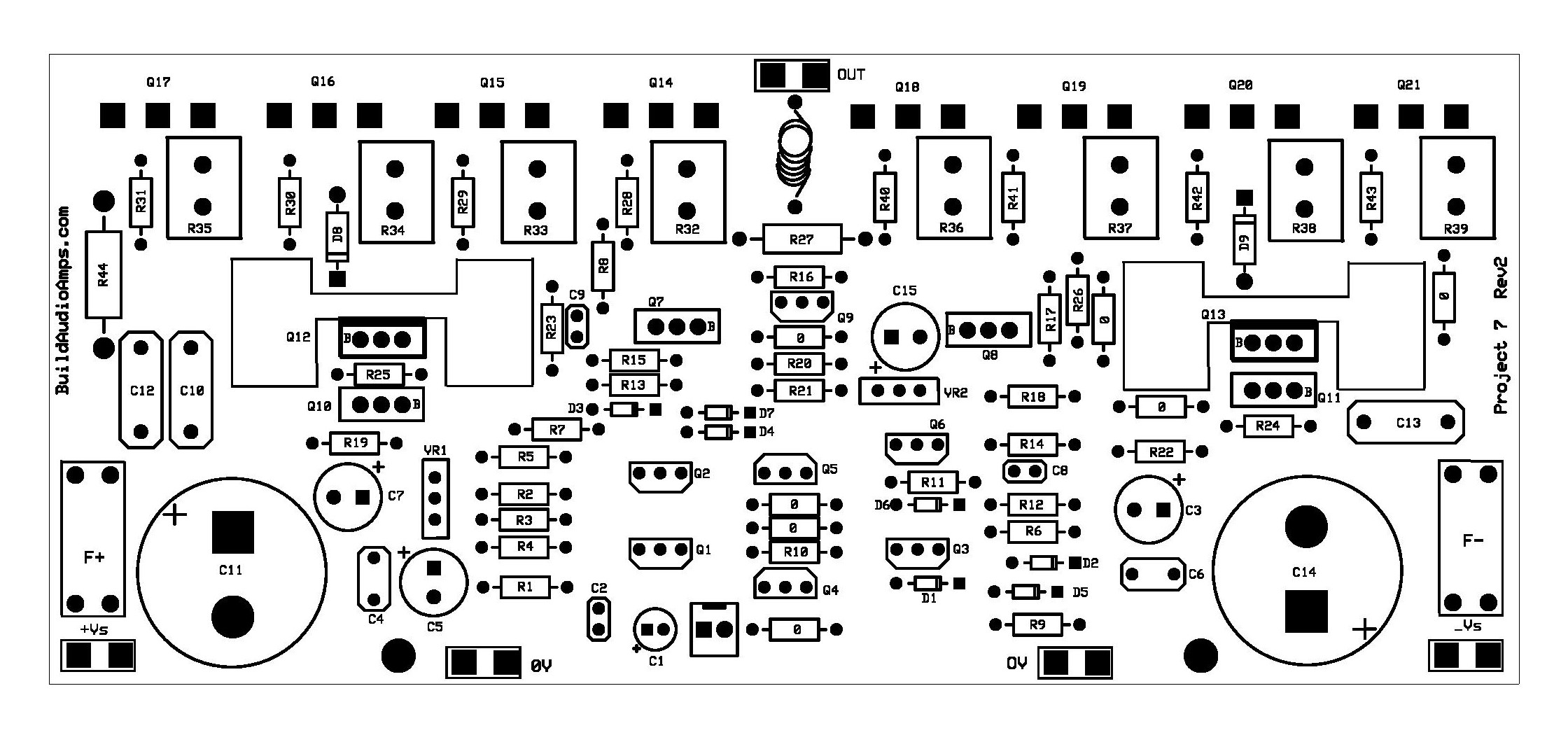
Project 7 Top Silkscreen Parts Placement Layer
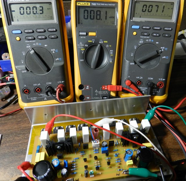
After you completed the printed circuit board assembly, it is time to do some testing and adjustments. Connect a shunt or shorting jumper at input of the amplifier as seen in the next picture. A +/-30VDC power supply was used for testing this project. Make sure all DMMs are connected as shown in the preceeding pictures. Turn power ON. The white (output) and green (ground) test clips are connected to the DMM on the left of the picture reads 0.3mV the DC offset voltage of the amplifier.
The offset can be adjusted to decrease by turning VR1 clockwise. The red and black test clips at +Vs fuse terminals are connected to the DMM on the right reads the current of 71mA. This is dependent on the setting of VR2. The red (Q17 emitter) and green (Q21 emitter) test clips are connected to the DMM in the middle reads 8.1mV, the voltage drop across the emitter ballast resistors. It can be adjusted to increase by turning VR2 counter clockwise.
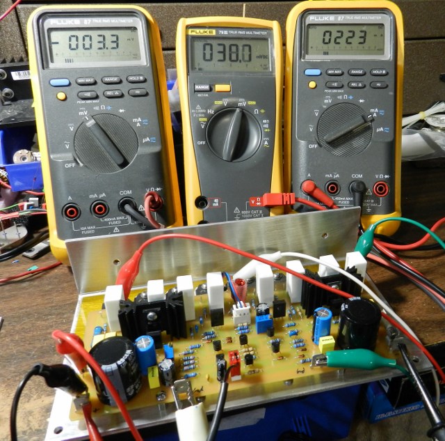
Readjust readings after a warm-up period of about 30 minutes. If you obtained different readings, switch the power supply to OFF immediately and check for assembly errors, the usual stuff.
During music test, at normal listening level, you should have similar DMM readings as shown in the next picture.
What do I listen for music test? Download Guaji-Rita by Hector Martignon from Allegro 2011 Winter Sampler album, Bossa de Mank by Claudio Roditi from Allegro Fall 2011 Sampler album, Renewal by Monty Alexander and Bluesy Basie by Rossano Sportiello from Allegro Spring 2011 album and a techno album from Iboga Records Amazon Sampler (play the Sao Paulo cut). I paired this project with the LM1036 tone control project and the music selections mentioned sounds great with Project7!
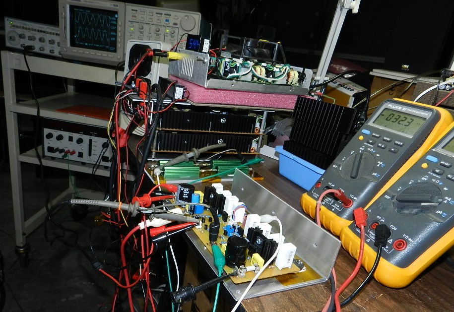
Let's do some more testing to Project 7, this time a ±54VDC SMPS, a Tektronix TDS520D oscilloscope, an HP3312A function generator and an 8Ω 400W "shop-built" dummy load was used.
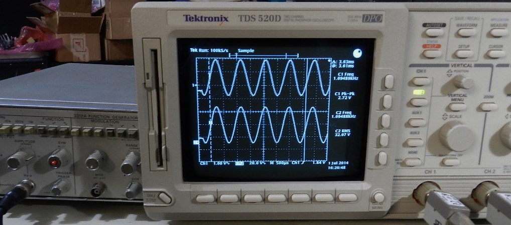

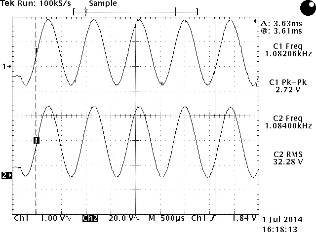
The function generator was set at 1KHz about 2.92Vpp sine wave output signal, it produces a 32.98Vrms across an 8Ω 400W load resistor with a small clipping on positive peaks, as shown in the middle picture. The power output is about 136Wrms. Decreasing the input signal to about 2.72Vpp to eliminate clipping, produces about 32.28Vrms across the load or a power output of about 130Wrms.