Project 25
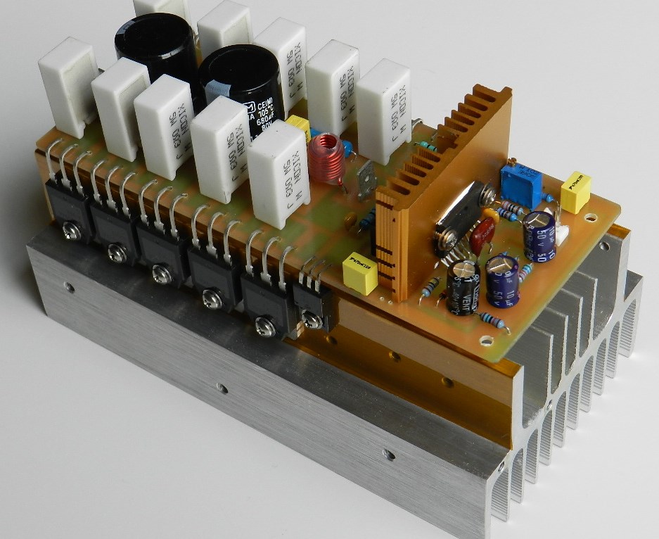
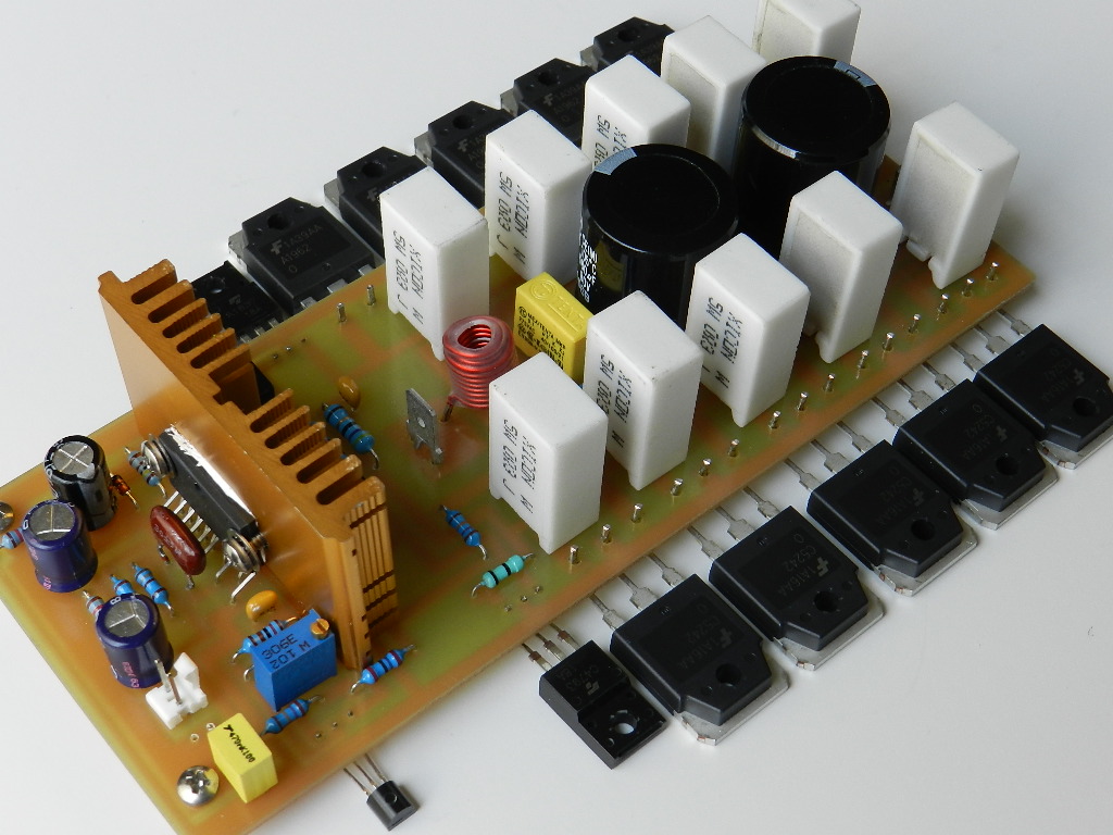
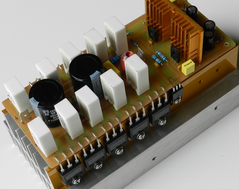
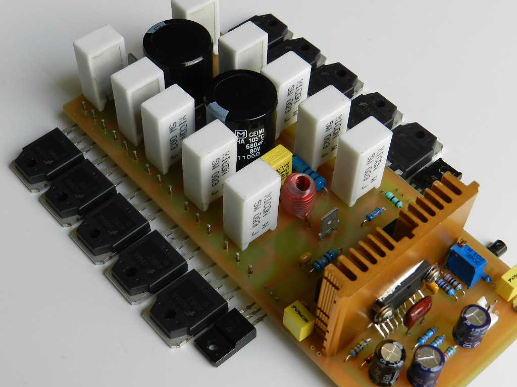
Project 25 is yet another power amplifier project with an LME49811 input stage driving a 3-stage emitter-follower output stage. The output stage consists of Q1 and Q8 as pre-drivers, Q2 and Q9 as drivers for the paralleled five pairs of complementary T03P-packaged power output transistors, Q3 thru Q14. Single shared emitter resistors are at the pre-driver and driver stages operating in Class A mode. The addition of a pre-driver stage provides current gain and buffers the LME49811’s output from the driver stage. Multilayer ceramic capacitors, C5 and C6, were added to the pre-drivers for high frequency compensation and to improve overall stability of the amplifier. I’ve decided to use five pairs of complementary power output transistors, so that higher current is available and better heat dissipation when driving a 4Ω and particularly with 2Ω loads. The power output of Project 25 was measured at about 220Wrms into an 8Ω load with a ±64VDC power supply.
The two through-hole locations labeled “Gnd” on the silkscreen layer of the PCB is for a piece of 20AWG hook-up wire, cut about 3 inches, to connect the ground of the input and output stage together and soldered at the bottom side of the PCB. There are two suggested power output transistor-mounting styles for this project as shown in the heading pictures above. The schematic diagrams, BOM and PCB layout for Project 25 are available for free by request, as is, no warranty.
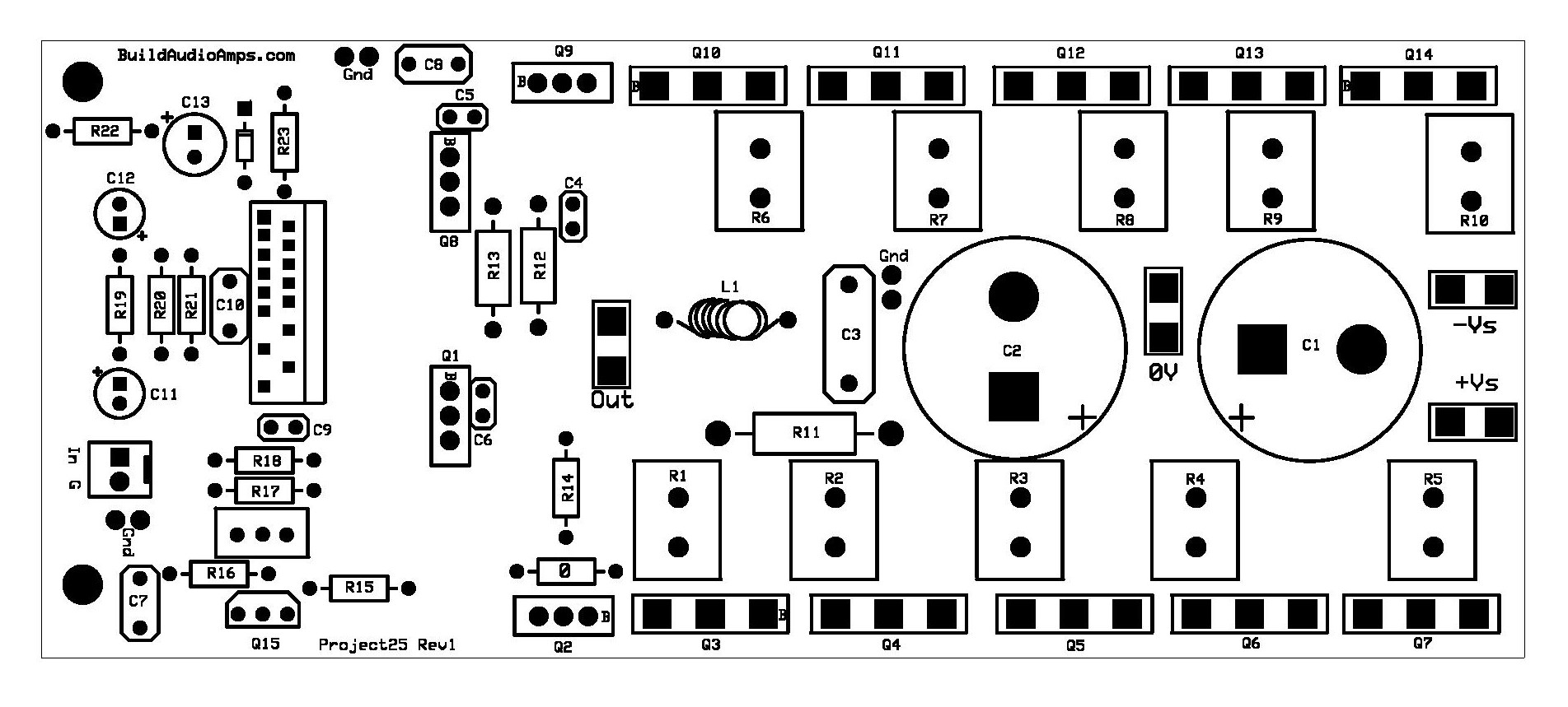 Project 25 Silkscreen parts placement layer of PCB.
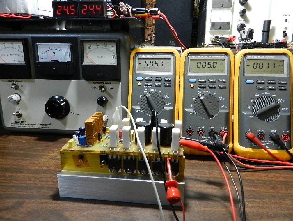
Here’s the fun part! Insert a jumper or shunt at the input of the amplifier. Do not connect any load or loudspeaker at the output of the amplifier. Adjust VR1 for minimum resistance. Prepare 3 DMMs to measure the DC offset voltage, the voltage between the emitters of Q7 and Q14 power output transistors and the current between the +Vs PCB terminal and the positive rail of the power supply. A safe way of powering up your newly built project the very first time is to use a ±24VDC power supply or whatever low-voltage dual-polarity power supply that you may have. If something goes wrong with your project, there will be minimal or no damage at all to the populated components!
The picture on the left with a ±24VDC power supply shows the DC offset voltage at 5.7mV measured at the output of the amplifier, 5mV across the emitters of Q7 and Q14 and the current measured between +Vs PCB terminal and positive rail of the power supply at 77mA. Carefully adjust VR1 to obtain the 5mV reading after a warm-up period of about 10 minutes. If you get different DMM readings, switch the power supply to OFF immediately and check the PCB for assembly errors.
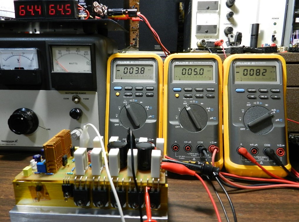
If a Variac transformer is available, connect the AC input of the power supply to the output of the Variac transformer. Switch the power to ON and gradually adjust the Variac’s AC output voltage from zero until the voltage output of the power supply reaches ±64VDC while keeping an eye on sudden increase in any DMM readings. If you have observed an increase in any of the DMM readings, switch the power to OFF immediately and check for PCB assembly errors. The picture on the right with a ±64VDC power supply shows a DC offset voltage at 3.8mV, the voltage across Q7 and Q14 at 5mV and the current between the +Vs PCB terminal and positive rail of the power supply at 82mA. Readjust VR1 to get the 5mV reading after 10 minutes, after that, you may proceed with music test!
If a Variac transformer is unavailable, make sure that the power supply has been properly built and that the output voltage rails have been measured at ±64VDC before connecting it to the project. With the power supply at OFF, adjust VR1 for minimum resistance. Switch the power supply to ON; the DMM measuring the voltage across Q7 and Q14 should read less than 1mV. If the DMM reading is more than 1mV and cannot be adjusted, power OFF immediately and check for PCB assembly errors. If the DMM reading is less than 1mV, wait for 10 minutes for the bias to stabilize and then carefully adjust the reading to 5mV, after that, you may proceed with music test!

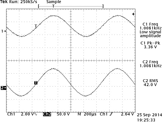
The next test procedure is optional, but if an oscilloscope, audio signal generator and 8Ω dummy load are available, the maximum power output before clipping occurs can be measured. Be extra careful not to touch the heat sink or the dummy load during this test; they will get extremely hot! After building Project 21, I’ve improved the dummy load’s heat sink and added more series-parallel connected power resistors for a total resistance of 8Ω and combined power rating of 700watts.
The power output was measured using an HP3312A Function Generator set at 1KHz 3.36Vp-p sine wave output and connected directly to the input of the amplifier under test as well as the CH1 test probe of the oscilloscope. An 8Ω/700Watt dummy load was connected at the output of the amplifier under test as well as the CH2 test probe of the Tektronix TDS520D 500MHz Digital Phosphor Oscilloscope. The amplifier produces 42Vrms across the 8Ω/700W dummy load or a power output of about 220Wrms, as shown in the TEK hardcopy picture on the right. The oscilloscope’s horizontal scale was adjusted at 200uS to verify for any visible clipping or artifacts on either peak. A forced air-cooling is recommended for this project for long-term reliable operation. This project was paired with Project 9, the LM1036 tone control project.