Project 17
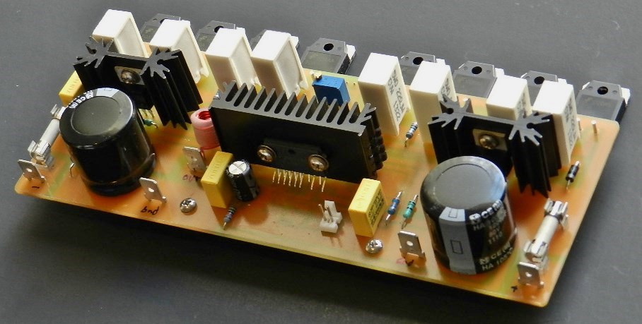
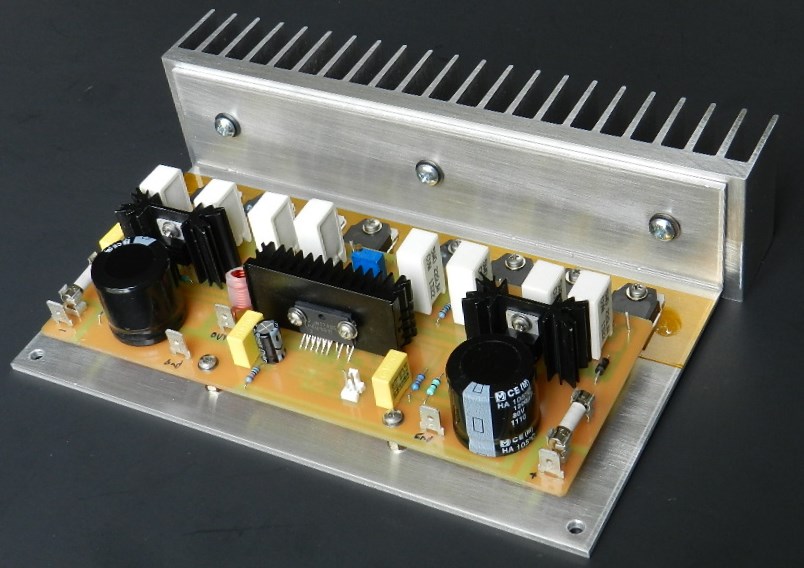
Project 17 is another audio power amplifier project that uses the LME49811 as the input stage and the power output stage consists of TO-126 and TO-220 packaged BJT drivers connected to 4 pairs of TO3-P packaged power MOSFET devices. The BJT drivers are configured as emitter-followers similar to the popular Locanthi T-circuit. The power output MOSFETs are configured as source-followers. This project is rated at 200Wrms into an 8-ohm load with a ±64 to ±70VDC power supply rails. You maybe interested in the LME49830, compatible to drive almost any power MOSFETs directly.
A couple of SMDs were combined with the rest of the through-hole components to simplify copper trace runs on the PCB layout and challenging to build! The SMD types are noted in the Part Value column of the bill of materials and matches with the Part IDs on the PCB. The PCB layout and Project 17 BOM are provided for free by request, as is, no warranty.
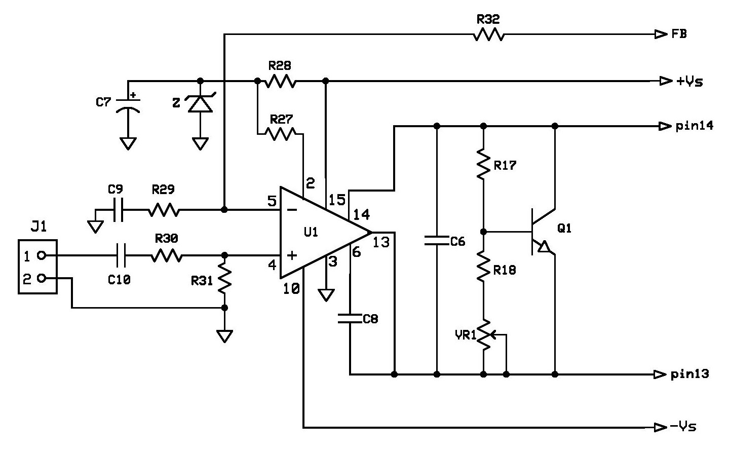
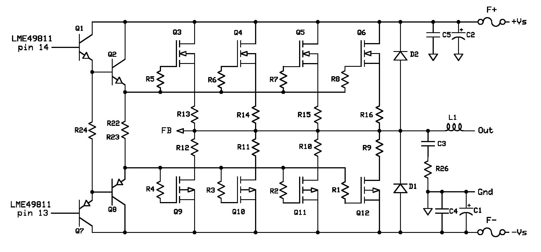
Schematic diagram of LME49811 Input Stage. Schematic diagram of the output stage using BJT and power MOSGETs.
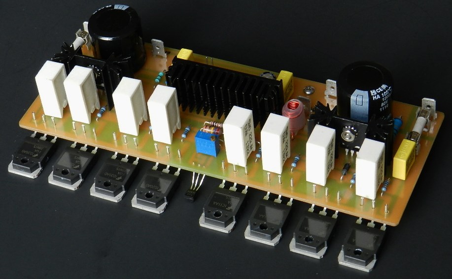
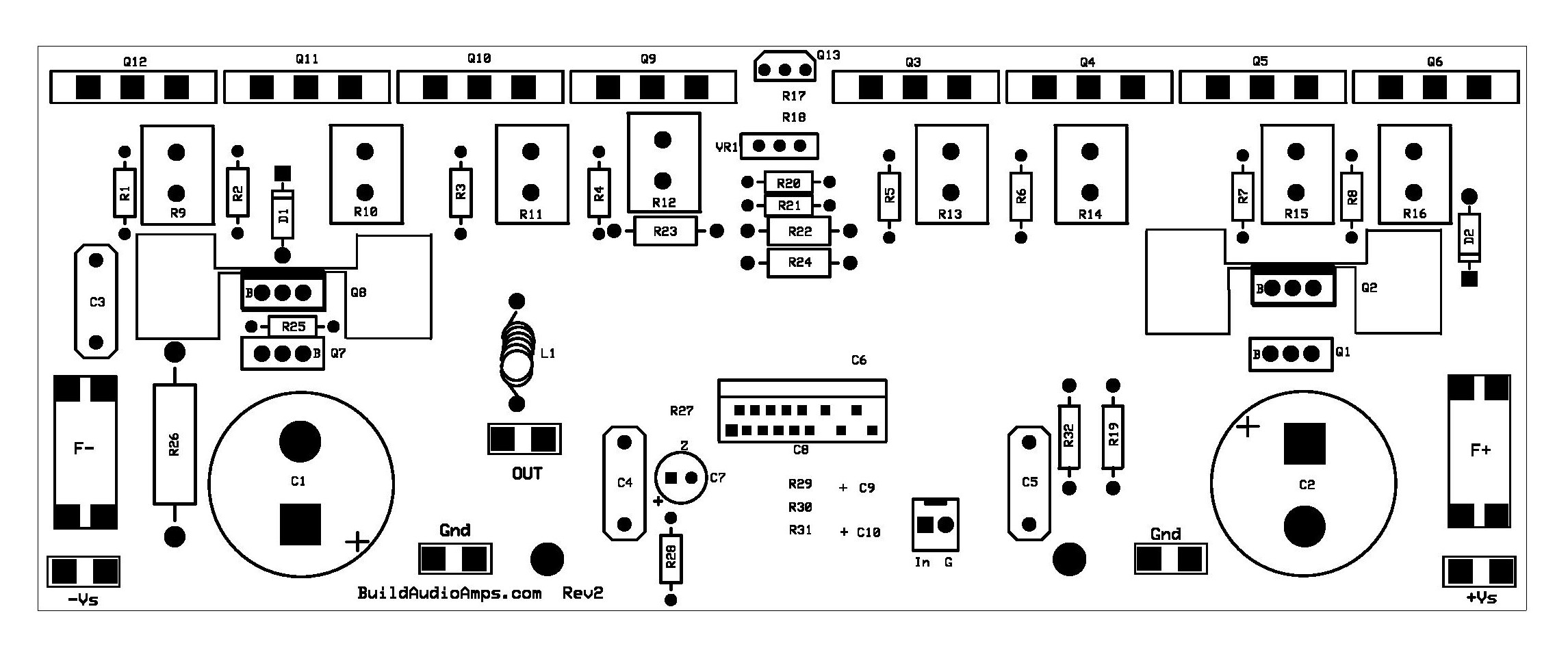 Silkscreen parts placement layer of PCB.
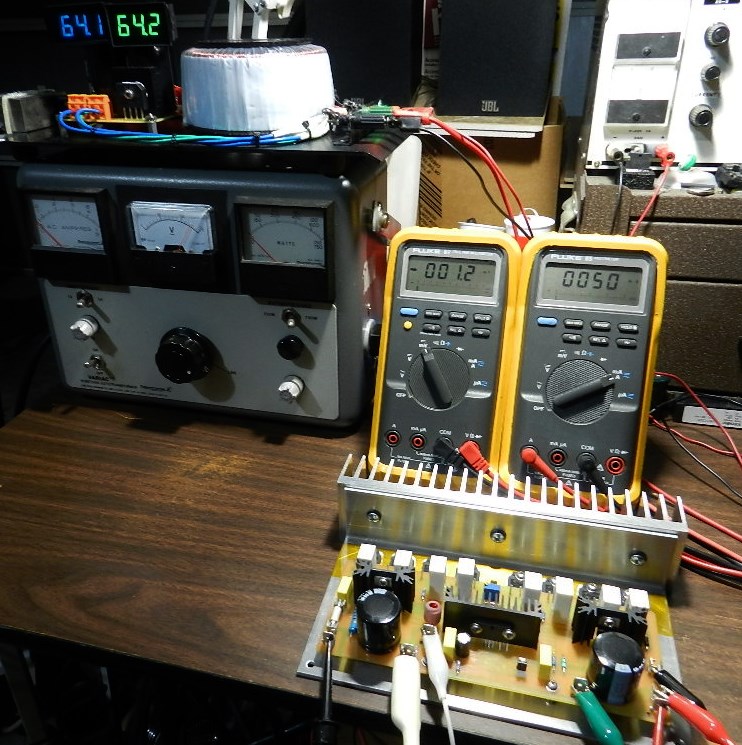
Here comes the fun part. Install a shunt at the input and do not connect any load at the output of the amplifier under test. If a Variac is available, initially power the amplifier at ±24VDC. Adjust VR1 to obtain about 50mA across the F+ fuse terminals after a warm-up period of about 10 minutes. The DC offset voltage is about 1.2mV. Other than those readings, switch OFF the power supply immediately and check for PCB assembly errors. Otherwise proceed with the next step.
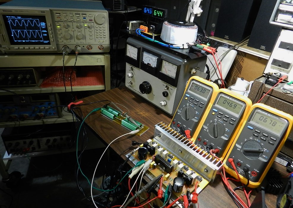
Another DMM was added to the test setup to measure the voltage drop across source resistors R9 and R16. Gradually increase the voltage up to ±70VDC while observing the AC ammeter and wattmeter readings on the Variac. Carefully readjust VR1 to obtain about 50mA across the F+ fuse terminals. Any sudden change or increase in DMM or Variac meters' reading, switch OFF the power supply immediately and check for PCB assembly errors. If no problems were encountered, proceed with music test. This project was auditioned with the LM1036 tone control project and does not disappoint.

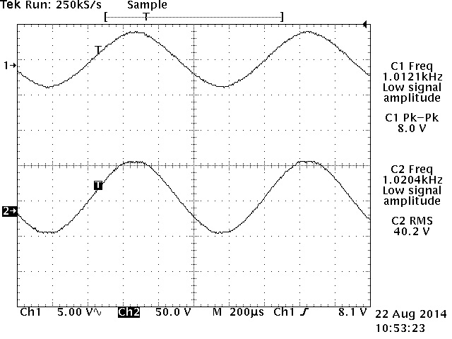
The next step is optional, but if you have the equipments to perform the test, proceed with power output measurement. Be careful not to touch the amplifier’s heat sink or dummy load, they will get extremely hot during this test. The power output was measured using an HP3312A Function Generator set at a sine wave 1KHz 8Vp-p output and connected directly to the input of the amplifier under test as well as CH1 test probe of the oscilloscope. An 8Ω/400Watt dummy load was connected at the output of the amplifier under test as well as CH2 probe of the Tektronix TDS520D 500MHz DPO.
The amplifier produces a 40.2Vrms across the 8Ω/400W load or a power output of about 200Wrms, as shown in the TEK hardcopy pictures. Higher power can be obtained with 4Ω or 2Ω loads. The horizontal scale was adjusted at 500uS for the test result picture on the left and 200uS on the right, to verify for any visible clipping on its peaks. Enjoy!
Updated 11-17-2014
On BOM R22 and R23 should be 27.4Ω 1/2W x 2 in series.