Project 33
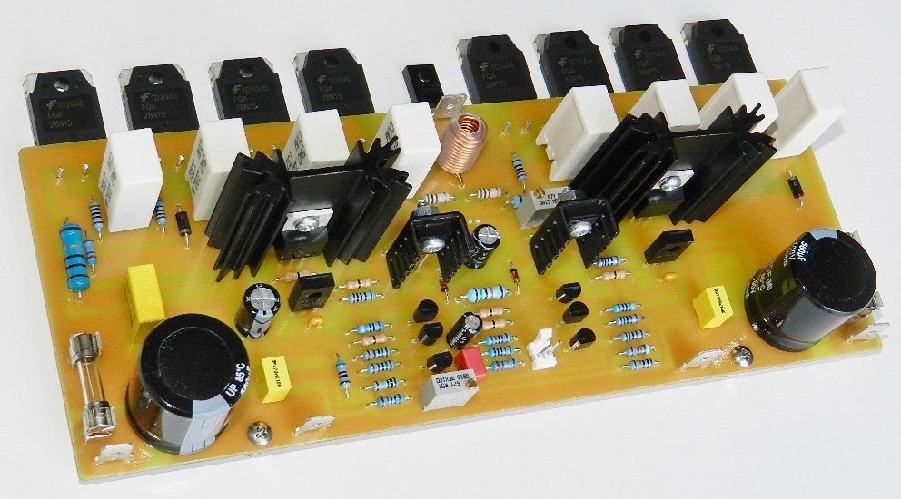
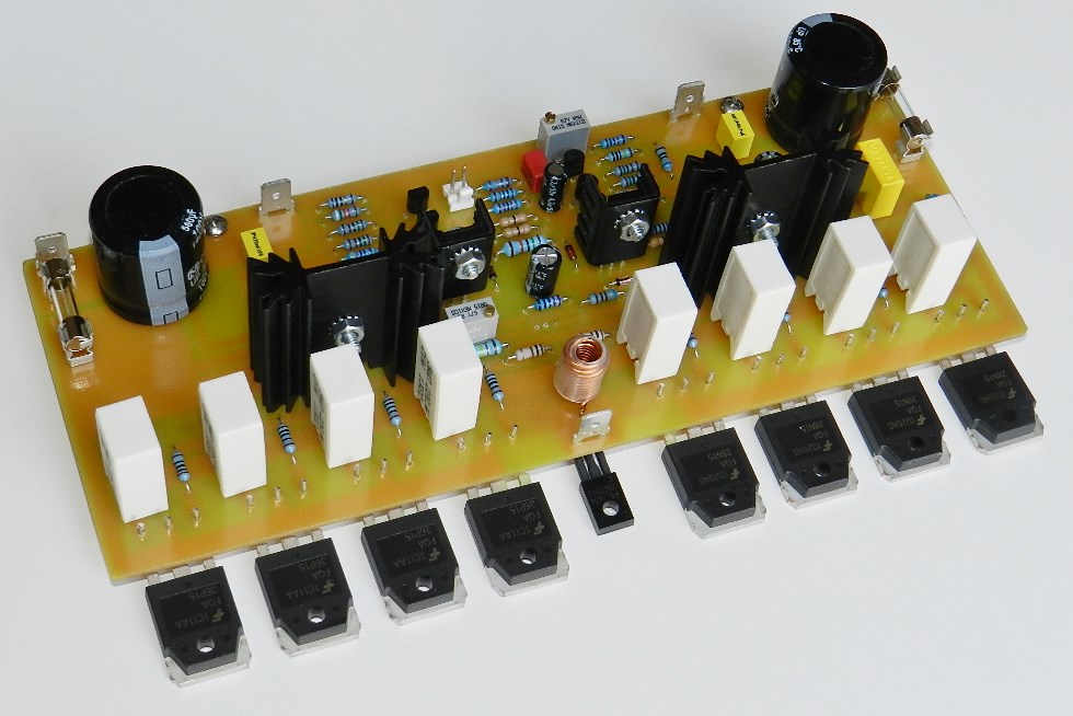
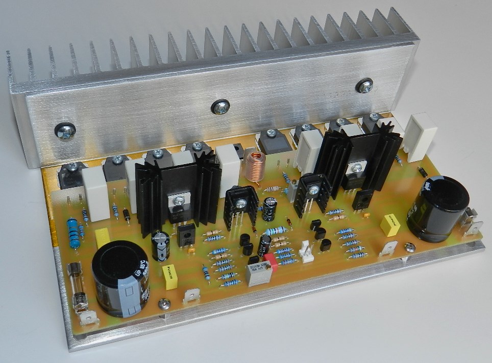
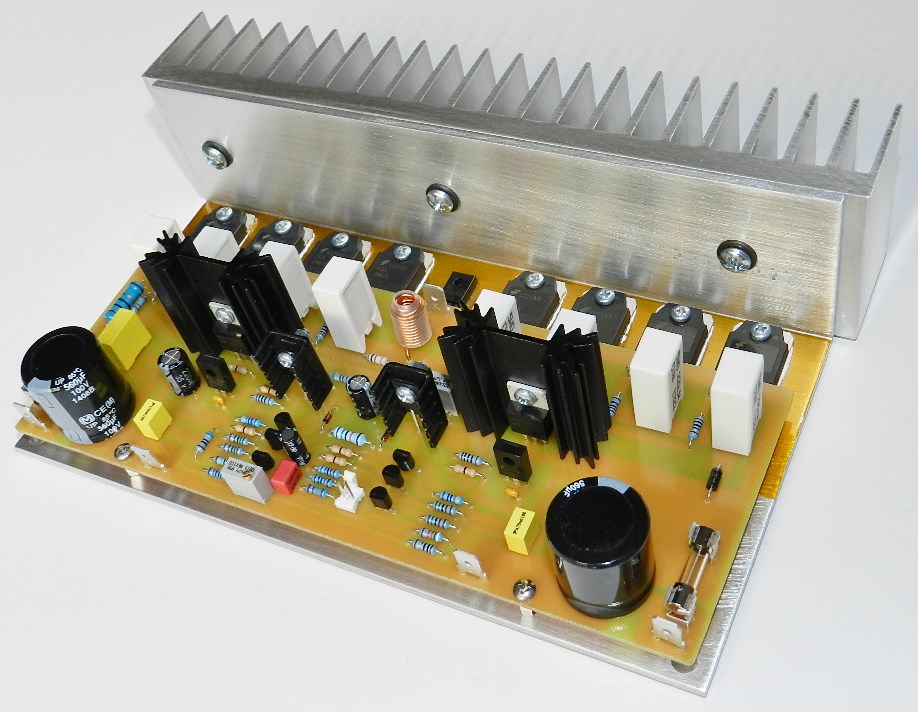
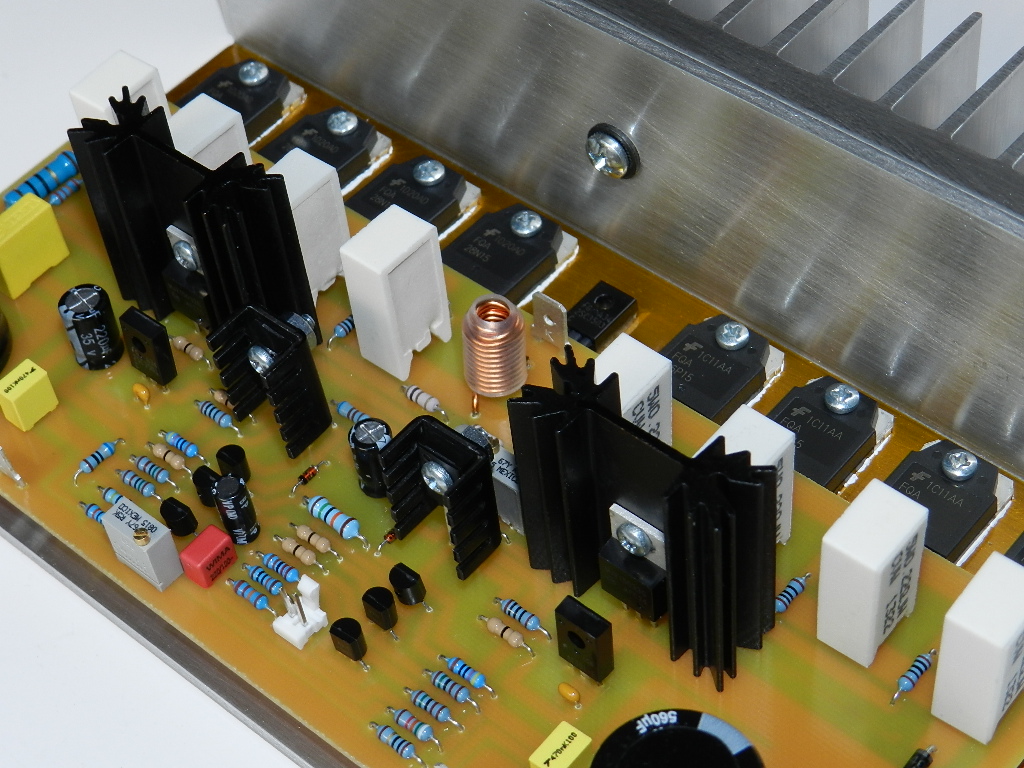
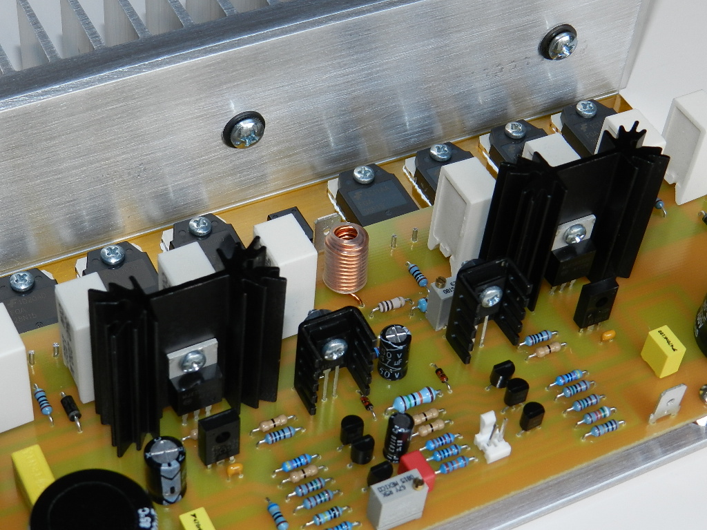
The input stage of Project 33 is the same complementary-symmetrical topology from previous projects but the power output stage this time are power MOSFETs. The source-follower output stage utilizes Fairchild Semiconductor’s QFET Power MOSFETs rated at 150V of drain-source voltage, more than 30A of drain current, identical RDS(on) of 90mohms and more than 200watts of power dissipation. These enhancement mode power MOSFETs are especially tailored by Fairchild’s advanced technology to reduce on-state resistance and high avalanche energy strength suitable for audio amplifiers and other applications. Project 33’s measured power output is about 178 watts with ±65VDC power supply rails into an 8Ω load. Higher power output is attainable with 4Ω or 2Ω load. The prototype model was tested with a 3Ω loudspeaker and produces firm, clean bass inherent to most audio amps that are using power MOSFETs.
If you are interested in building this project and have read the Information and Policies section of this website, the schematic diagram, PCB layout (available only by request) and BOM are free, as is, no warranty.
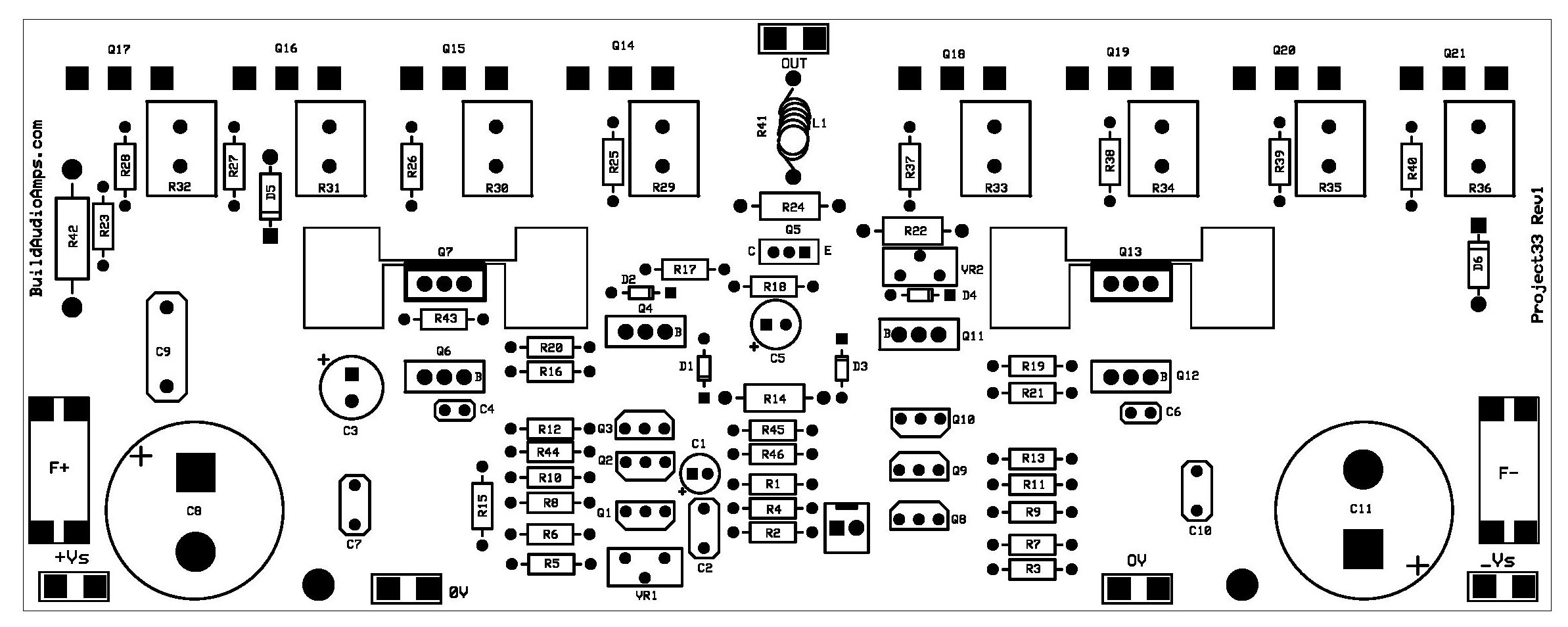
Silkscreen Parts Placement Layer of PCB for Project 33.
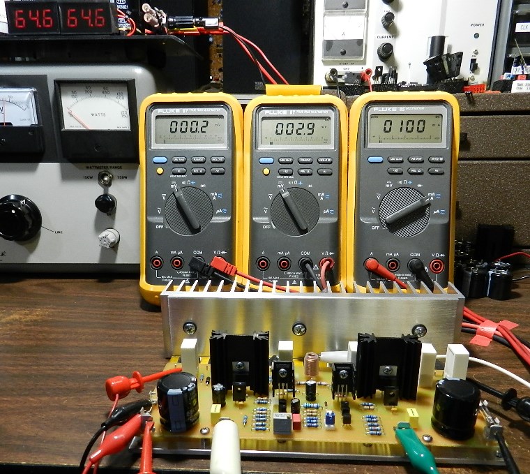
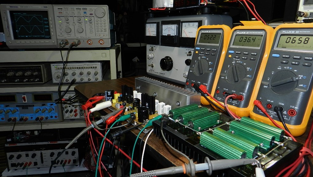
If you’ve decided to build this project, the DC offset voltage and the idle current need to be adjusted first before going into music test. Insert a jumper or shunt at the input of the amplifier. Do not connect any load or loudspeaker at the output of the amplifier. Adjust VR2 to maximum resistance of 5KΩ; please refer to schematic diagram where to access VR2 on top of PCB. Prepare 3 DMMs to measure the DC offset voltage at the output of the amplifier, the voltage between the sources of Q17 and Q21 power output transistors and the current across the F+ fuse terminals.
If a Variac transformer is available, connect the AC input of the power supply to the output of the Variac transformer. Switch the power to ON and gradually increase the Variac’s AC output from zero until the voltage output of the power supply reaches approximately ±64VDC. If you have observed a sudden increase in any of the DMM readings, switch the power to OFF immediately before any populated component vaporizes and check the PCB for assembly errors. The picture above shows a DC offset voltage at 0.2mV; adjust VR1 to get to this value. The voltage across the sources of Q17 and Q21 is measured at 2.9mV and this DMM reading could be anywhere from 2mV to 5mV. The current across the F+ fuse terminals measured about 100mA, adjust VR2 to get this value and could be anywhere from 90mA to 120mA. If you obtain similar DMM readings, you may proceed with music test.
If a Variac transformer is unavailable, make sure that the power supply has been properly built and that the output voltage rails have been measured at approximately +/-64VDC before connecting it to the project. With the power supply at OFF, adjust VR2 for maximum resistance. Switch the power supply to ON; the DMM measuring the voltage across Q17 and Q21 should read less than 1mV. If the DMM reading is more than 1mV and cannot be adjusted by VR2, power OFF immediately and check the PCB for assembly errors. If the DMM reading is less than 1mV carefully adjust the reading from 2mV to 5mV. The current across the F+ fuse terminals will also vary from 90mA to 120mA. Adjust the DC offset voltage thru VR1 for minimum or within ±10mV DMM reading at the output of the amplifier. If you obtain similar DMM readings, you may proceed with music test.
The next test procedure is optional, but if an oscilloscope, audio signal generator and 8Ω dummy load are available, the maximum power output before clipping can be measured. Be careful not to touch the heatsink or the dummy load during this test, they will get very hot!
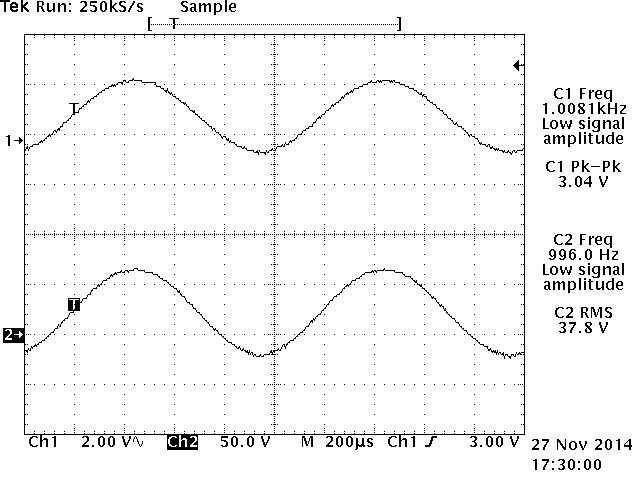
The power output was measured using an HP3312A Function Generator set at 1KHz 3.04Vp-p sine wave output and connected directly to the input of the amplifier under test as well as the CH1 test probe of the oscilloscope. An 8Ω/700Watt dummy load was connected at the output of the amplifier under test as well as the CH2 test probe of the Tektronix TDS520D 500MHz DPO. The amplifier project produces 37.8Vrms before clipping across the 8Ω/700W dummy load or a power output of about 178 watts, as shown in the TEK hardcopy picture on the right. The oscilloscope’s horizontal scale was adjusted at 200uS to verify for any visible clipping or artifacts on either peak. This project was paired with Project 9, the LM1036 tone control project.