
Project 13

The power output stage circuit of Project 13 originated from SAE’s vintage product, the MK25/2500 power amplifier. After completing Project 12, a valid question came up: was there any upgrade circuit with considerable power to the basic Ampzilla’s design? I came across a SAE power amplifier circuit, which is similar to Project 12, but had a more robust power supply at ±95VDC and 4 pairs of complementary power output devices. The designer of the Ampzilla, James Bongiorno, also worked with SAE during that era. I also found out that SAE’s parent company filed for bankruptcy in the ‘90s, but audiophile fans of their products are still active.
SAE called the added drivers and output devices as positive and negative slaves. It would be similar in concept to ST ‘s modular application of several TDA7293. If you visualize removing Q3~Q5 for positive and Q9~Q11 for negative slaves, the circuit would look like this:
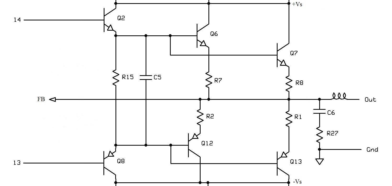
The drivers as well as the power output transistors are basically an emitter-follower circuit as compared to Ampzilla’s Darlington pair-inspired design. The voltage divider resistors connected at the base of the drivers to the +Vs and –Vs rails are still being used in both designs. Here's the schematic diagram of Project 13:

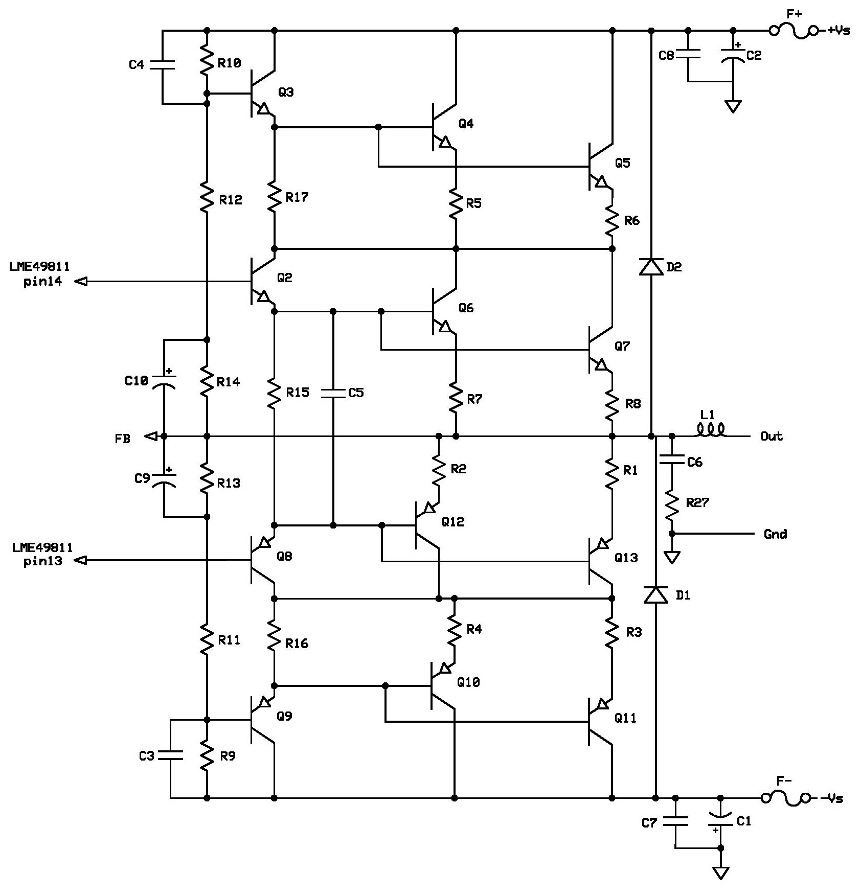
Input stage of Project 13 using LME49811 Power output stage of Project 13 using Mark25
Let’s go ahead build this amp and see how it compares to Project 12. I’ve decided to use 2 pairs of T0220 drivers and 4 pairs of T03P output transistors. The LME49811 input stage schematic is the same as in Project 12 but the Part IDs and some values were changed as shown in Project 13 BOM.
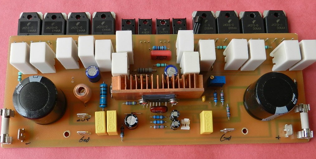
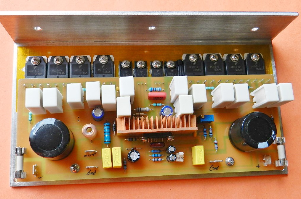
 Project 13's Silkscreen Parts Placement Layer of PCB
Make sure to connect “y>” to “<y” (2 places) together, by soldering 2 pieces of 18AWG hook-up jumper wires as indicated on top silkscreen layer of PCB. This connects the copper traces of R1/R2 and R7/R8 together, please refer to the schematic diagram.
After completion of the circuit board assembly, using an ohmmeter adjust VR1 counterclockwise to measure across its terminals the minimum resistance or 0Ω. It can be accessed on top silkscreen layer of the PCB at opposite ends of R33 and R34. Install a shunt jumper at J1 input and do not connect any load at the output. A ±54VDC power supply was used to initially power-up the project. If available, just to be safe, I would recommend using a ±24VDC power supply for initial testing. With the power OFF, remove F+ fuse and insert a milliammeter at its terminals. Connect a millivoltmeter at the output and ground terminals. Switch power supply to ON.
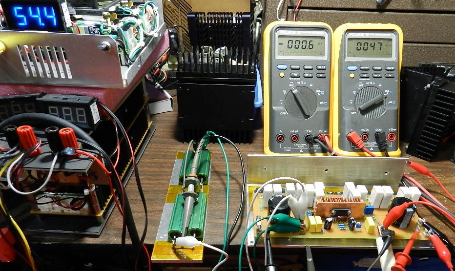
The DMM on the left side of the picture is reading the DC offset of the amplifier at 0.6mV. The DMM on the right side of the picture is reading 47mA the current drawn by the amplifier. If you obtain different readings, power OFF immediately and recheck PCB for assembly errors. If the problem was corrected proceed with the next step.
With the power supply at OFF, connect another millivoltmeter at the emitter of either Q6 or Q7 and output terminal of the amplifier. The millivoltmeter will be measuring the voltage drop across R7 or R8. The voltage drop reading multiplied by the value of the resistor is equal to the idle current of the power output transistors.
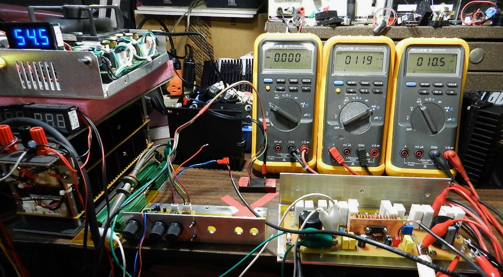
I have removed the shunt jumper and connected a test pre-amp at the input of the amplifier. Switch the power supply to ON for a warm-up period of 30 minutes. The DMM on the left side of the picture is measuring the DC offset of the amplifier at 0.000V, very impressive! The DMM in the middle of the picture is measuring the current drawn by the amplifier at about 120mA. The DMM on the right side of the picture is measuring the voltage drop of emitter resistor at about 10mV. This reading can be obtained by adjusting VR1 clockwise. If you made the same test results, then proceed with music test!
The next step is optional, but if you have an oscilloscope, audio signal generator and an 8Ω dummy load, you can check the power output of the amplifier before clipping occurs. It is recommended to add a small fan to cool down the amplifier under test and dummy load, it will get hot!
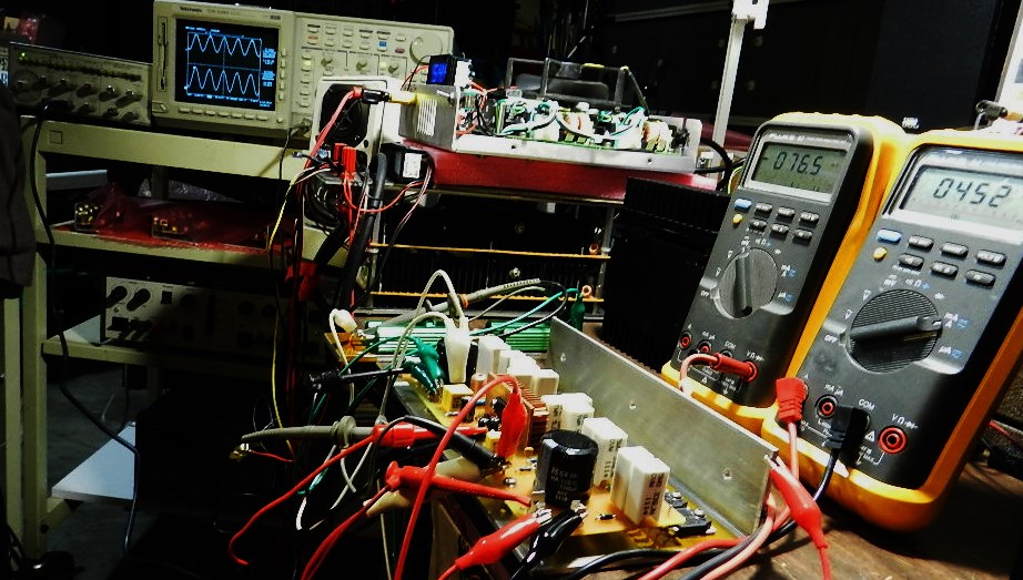
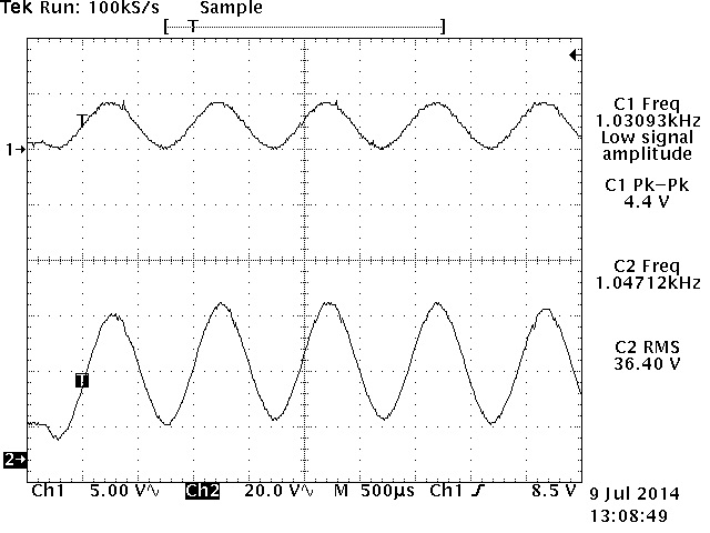
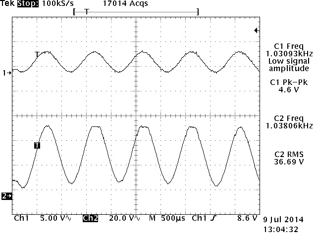
Applying a 1KHz 4.4Vp-p sine wave signal at the input produces a 36.4Vrms across the 8Ω/400W dummy load or a power output of 165.62Wrms. Increasing the same signal to 4.6Vp-p produces a power output of 168.26Wrms with a small clipping on positive peaks of the waveform. Enjoy!
![]()