Project 34
This is another build your own audio amplifier project. Erno Borbely’s excellent 60W MOSFET Power Amplifier design appeared as an audio amplifier construction project in Audio Amateur Magazine in February of 1982 and is the starting point for developing Project 34. It’s one of the 26 power amplifier projects found in the Audio Amateur Power Amp Projects book. The book is a compilation of interesting vacuum tube and solid-state power amplifier projects appearing in the obsolete Audio Amateur Magazine from 1970 to 1989. Is it worth revisiting the power amp design? We will see…
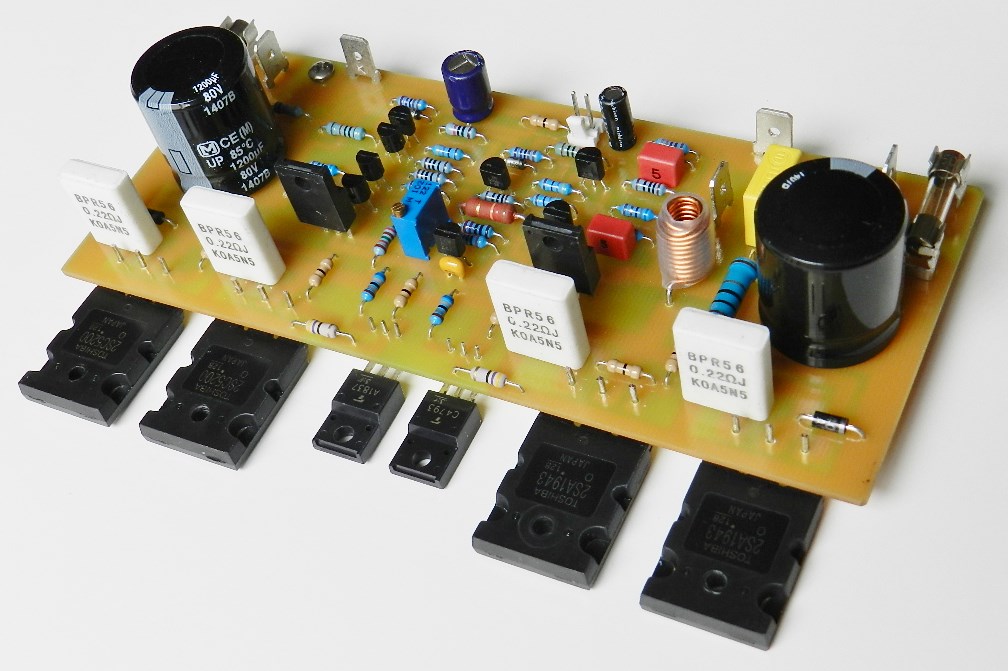
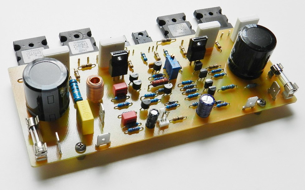
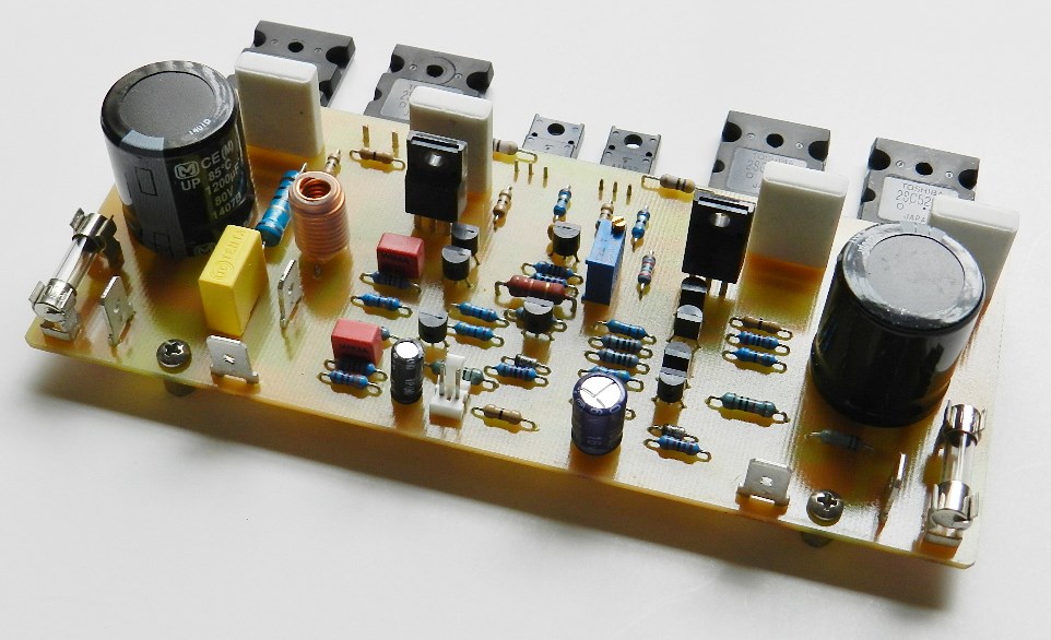
Erno called his audio power amplifier design as a double differential input amplifier whose outputs are connected to R. Lender’s voltage amplifier stage circuit. The power output stage uses MOSFETs; however this project utilizes power BJTs configured in a Complementary Feedback Pair topology. Several modifications were made to the original circuit so that it could properly match with the BJT output devices and at the same time make use of readily available components. The prototype model produces more than 100 watts of wonderful audio power into an 8Ω load with a ±50VDC power supply rails.
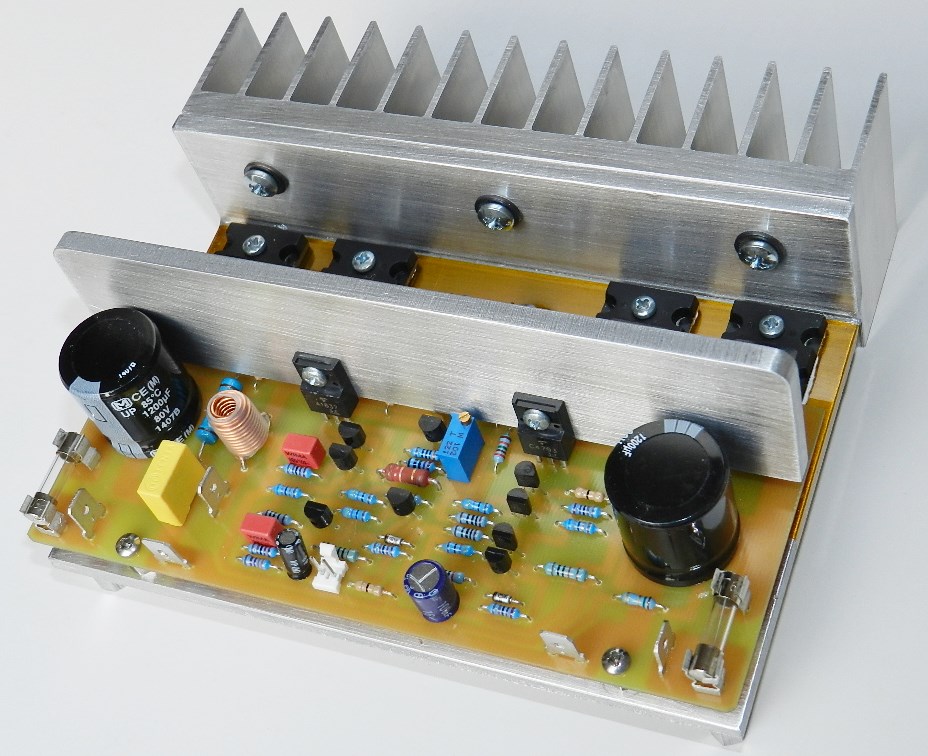
After a couple of blown fuses and parts these were the changes made to the original circuit, please refer to Project 34’s schematic diagram: Zener diodes, D1 and D2, were used in the current source circuits which was also described in the article. Biasing transistor, Q17, was replaced with an NPN transistor. Input resistor, R2, was increased to lower the DC offset voltage of the amplifier. Series-connected R20 and R35 have to be rated at 2-watts each because they tend to get very hot (you can smell it!), which was specified at 500mW in the original circuit. C5 and C7 have to be added to eliminate high frequency noise while improving the overall stability of the amplifier; this was the most significant addition to the original circuit. A piece of aluminum plate approximately 1.25” X 6” x 0.25”, as seen on the prototype model, serves as a heatsink for the voltage amplifier transistors Q5 and Q13.
The RC network in the global feedback path was removed; instead, a single feedback resistor, R21, was used and the value of R18 was increased that resulted to about 27 dB of AC-gain. This RC network, in my opinion, is the audio power amplifier designer’s tone signature. In other words, this complex arrangement of R and C strategically placed in the global feedback path determines the frequency response of the amplifier. This answers the question as to why this amplifier when compared to that amplifier sounded unique, in a good way! In the past, I’ve experimented with a phono preamp circuit around its RIAA equalization RC feedback network and altered their values and it could either extend the high frequency tone, lower bass response or improve the midrange vocal frequency range. If properly configured and tested the same feedback scheme manipulation could be done in the power amplifier stage as well. The same technique is commonly used by other audio power amplifier designs and it will be added as a feature in future projects. However, the end result is subjective in nature and will leave it up to the audio amp builder to either include this RC feedback network on their project or not.
Personally, if properly built and the bias correctly adjusted this audio power amplifier project is a worthwhile BuildAudioAmps’ experience. If you’re looking for a simple and excellent sounding 100-watt power amplifier, look no further: this is the project to consider! If you are interested in building this project and have read the Information and Policies section of this website, Project 34 schematic diagram, PCB layout (available only by request) and BOM are free, as is, no warranty.
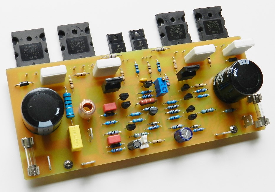
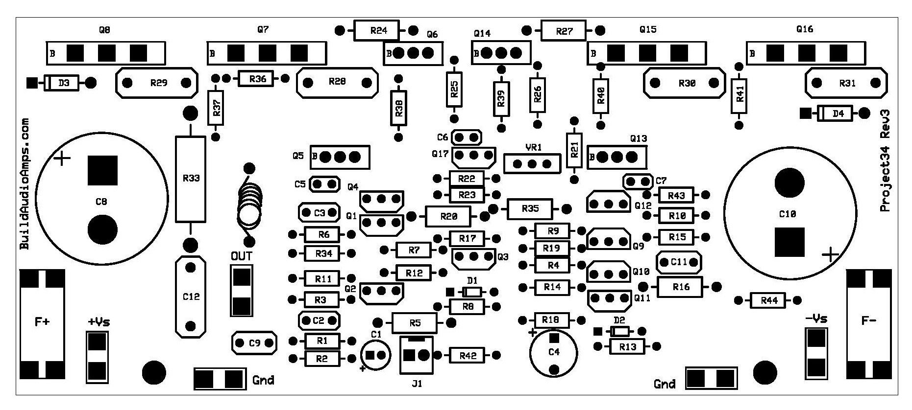 Project 34 Silkscreen Parts Placement Layer of PCB.
If you’ve decided to build this project, the idle current needs to be adjusted first before going any further. Insert a jumper or shunt at the input of the amplifier. Do not connect any load or loudspeaker at the output of the amplifier. Adjust VR1 to maximum resistance of 1KΩ; please refer to schematic diagram where to access VR1 on top of PCB. Prepare 3 DMMs; to measure the DC offset voltage at the output of the amplifier, the voltage drop of the emitter resistor in any of the power output transistors, Q7, Q8, Q15 or Q16 and the current across the F+ fuse terminals. Experienced amp builders have more than 3 DMMs.
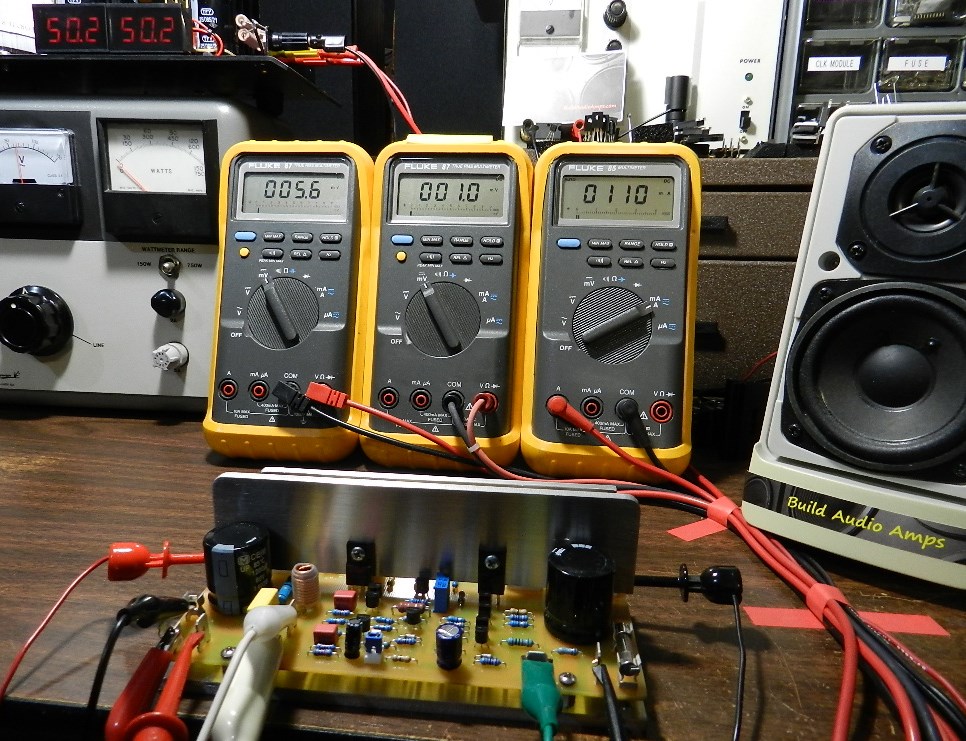
If a Variac transformer is available, connect the AC input of the power supply to the output of the Variac transformer. Switch the power to ON and gradually adjust the Variac’s AC output from zero until the voltage output of the power supply reaches approximately ±50VDC while keeping an eye on sudden increase in any DMM readings. If you have observed an abnormal increase in any of the DMM readings, switch the power to OFF immediately and check the PCB for assembly errors. The picture above shows a DC offset voltage at 5.6mV and this could be within ±10mV. The voltage drop across the emitter resistor is about 1.0mV after a warm-up period of 10 minutes; readjust VR1 to get a DMM reading from 1mV to 5mV. The current across the F+ fuse terminals is approximately 110mA, this value is dependent on the adjustment of VR1 and it is important to get to this value. If you obtain similar DMM readings, you may proceed with music test.
If a Variac transformer is unavailable, make sure that the power supply was properly built and that the output voltage rails have been measured at approximately ±50VDC before connecting it to the amplifier project under test. With the power supply at OFF, adjust VR1 for maximum resistance. Switch the power supply to ON; the DMM measuring the voltage drop across the emitter resistor should read less than 1mV. If the DMM reading is more than 1mV and cannot be adjusted by VR1, power OFF immediately and check the PCB for assembly errors. If the DMM reading is less than 1mV wait for 10 minutes for the bias to stabilize and carefully adjust the reading to 1mV, while the other DMM connected across the F+ fuse terminals, will read about 110~160mA of current. If you obtain similar DMM readings, you may proceed with music test.
To check if the bias was properly adjusted in both initial tests mentioned, switch the project’s power supply to OFF and allow the power amplifier under test to literally cool down for several minutes. With the DMMs in their original test locations, switch the power supply to ON. You will notice that the DMMs measuring the voltage drop across the emitter resistor and the current across the fuse terminals reads high but within the DMM’s range readings, please don’t panic! Allow the amplifier to warm-up and these readings will gradually go down from 1~5mV and 110~160mA.
The next test procedure is optional, but if an oscilloscope, audio signal generator and 8Ω dummy load are available, the maximum power output before clipping can be measured. Be careful not to touch the project’s heatsink, it will get very hot during this test!

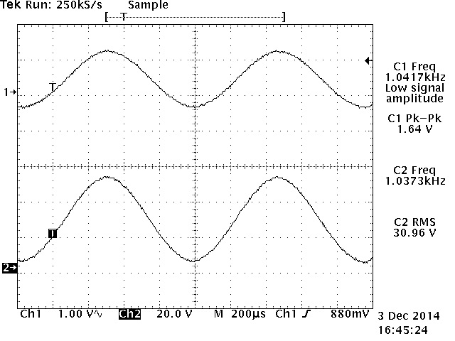
The power output was measured using an HP3312A Function Generator set at 1KHz 1.64Vp-p sine wave output and connected directly to the input of the amplifier under test as well as the CH1 test probe of the oscilloscope. An 8Ω/700Watt dummy load was connected at the output of the amplifier under test as well as the CH2 test probe of the Tektronix TDS520D 500MHz DPO. This power amplifier project produces 30.96Vrms across the 8Ω/700W dummy load or a power output of about 120W, as shown in the TEK hardcopy picture on the right. The oscilloscope’s horizontal scale was adjusted at 200uS to verify for any visible clipping or artifacts on either peak. This project was paired with a modified LME49720 tone control project; the audio quality reproduced was outstanding!