Project 39
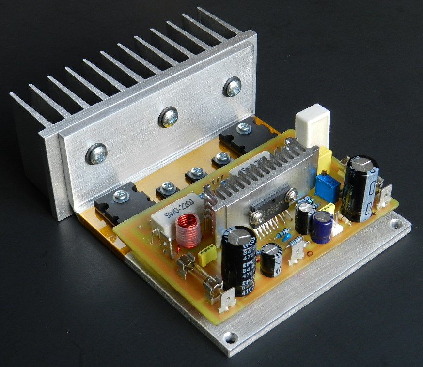
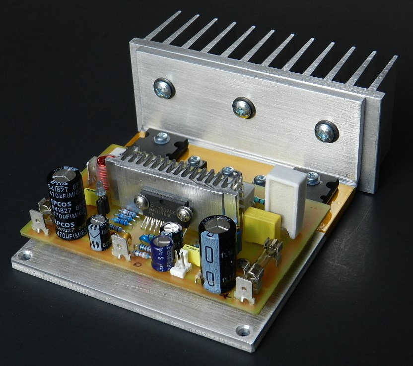
The concept of Project 39 is Texas Instruments’ LME49810 spec sheet SNAS391C, April 2013 revision. This audio amplifier input and driver stage chip have similar impressive specs like the LME49811. However, a unique feature of the LME49810 is the internal Baker Clamp and Clip Flag circuit. According to TI, the featured circuit insures that the amplifier power output devices do not saturate when over driven. The resultant “soft clipping” of high-level audio signals suppresses undesirable audio artifacts generated when the power output transistors are driven hard into clipping. When the output at pin 1 goes into clipping, a logic low level appears at the CLPFLAG pin.
The CLPFLAG pin can be used to drive an LED or other displays and on this project a 2-pin connector, J2, was added to access the circuit’s output at pin 1. If you plan to create your own PCB keep in mind that the CLPFLAG output is an open collector output; it should never be left to float under normal operation. If the CLPFLAG pin is not used, then it should be connected with a 1K resistor to the 5V reference voltage. On the prototype model a small blue LED was installed at J2, as shown in the heading pictures. During test, the clamp circuit on the prototype model was activated with an 18 to 20Vpp 1KHz sine wave input signal. This corresponds to a power output of more than 90 watts at 8Ω or 27Vrms across an 8Ω dummy load with ±49VDC power supply rails.
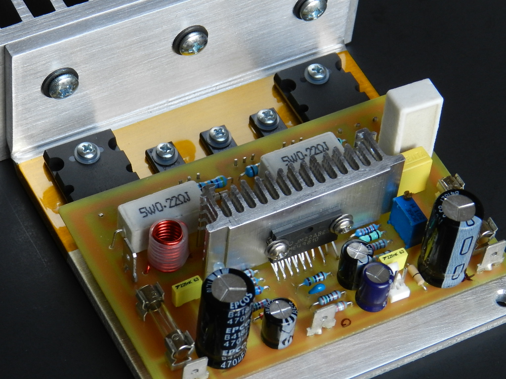
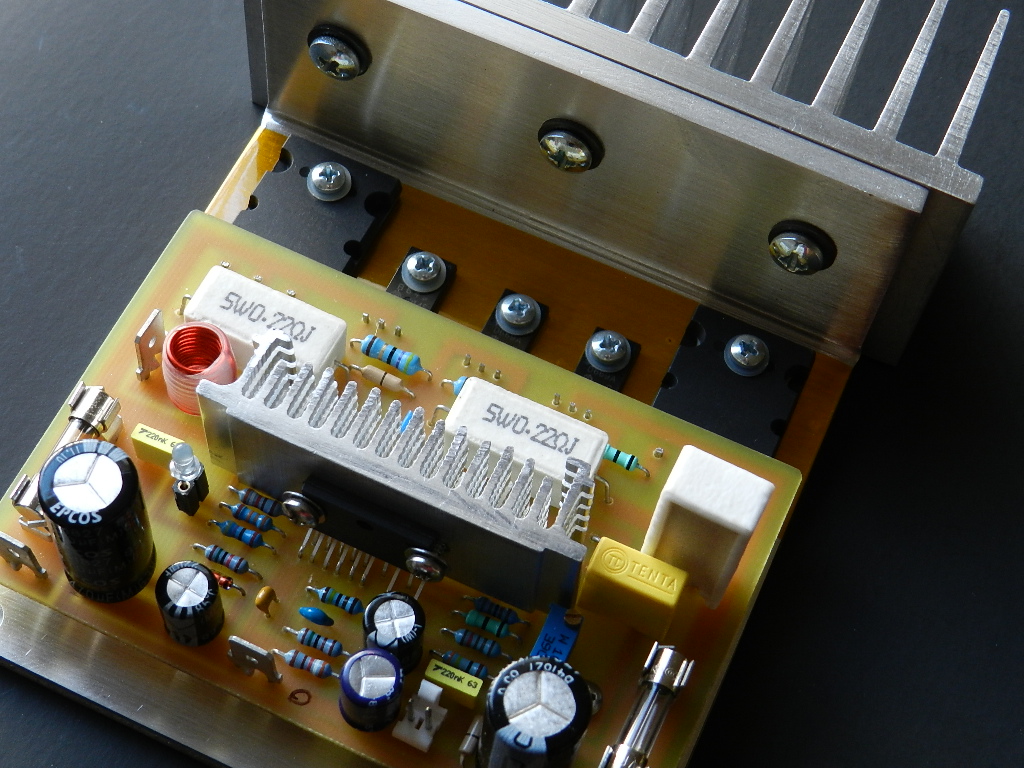
Other LME49810 features, electrical rating and characteristics are similar to the LME49811, except for two dedicated positive and negative external bias control pins. A VBE multiplier circuit consisting of Q1, VR1 and other associated components is connected at these pins. Q1 is preferably mounted on the same heatsink as the power output devices, to keep track of their temperature change. When the power transistors heat up, Q1 will reduce the bias voltage to compensate for the increase in temperature. This method prevents the power transistors from thermal runaway. Another method is to use emitter degeneration resistors, R13 and R14.
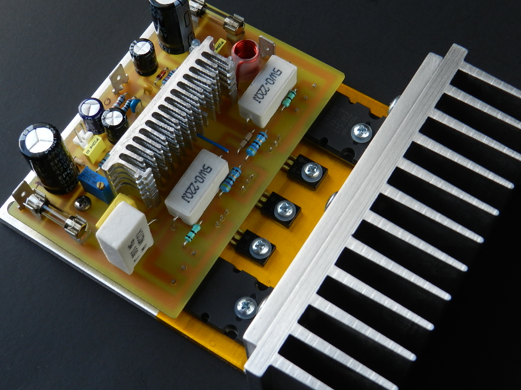
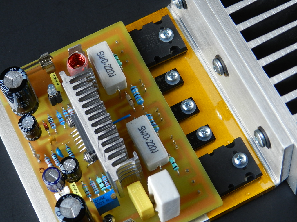
The project’s prototype model is based on the typical application schematic diagram on the SNAS391C spec sheet (Figure 1). Since this is a “how does this chip perform in real world” pilot project, it uses only a pair of T0-264 packaged complementary power output transistors driven by T0-126 packaged driver transistors. Succeeding LME49810 projects may evolve with different topologies and higher voltage rails that would correspond to increased power output. Currently, certain components were replaced in the typical application schematic for sonic improvement like the capacitor, Cf, in parallel with R3, which audibly improves the high frequency response of the amplifier. The resistor in series with a capacitor at the output (Zobel network) must be rated from 3W to 5W. Populated in the prototype is a 10Ω 5W radial resistor. The voltage gain of this project is about 29V/V (29.2dB), determined by the ratio of R5/R3; altering their values will change the voltage gain. Texas Instruments’ recommended voltage gain range is from 30dB to 40dB.
Here comes the most exciting part of this project. The project was matched with a modified LM49720 tone control preamp. While playing “Spanish Harlem” by Rebecca Pidgeon from Chesky Records’ Guide to Critical Listening album on a Toshiba HD-A2 player and Kenwood’s quad 12” 3-way speakers, there was spectacular clarity on the vocals with emphasis on the high frequency, percussion and details on bass. The entirety of Peter Gabriel’s “Scratch My Back” album was also played using the same setup to monitor its normal operating conditions. Project 39 performed very well with listening test.
If you are interested in building this project and have read the Information and Policies section of this website, the schematic diagram, PCB layout (available only by request) and BOM are free, as is, no warranty.
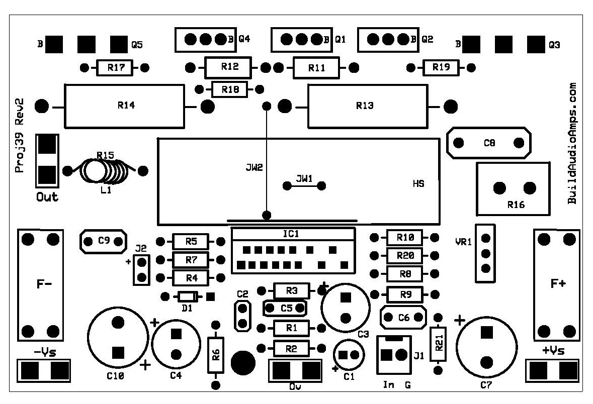
Project 39 Silkscreen Parts Placement Layer of PCB.
If you’ve decided to build this project, the idle current needs to be adjusted first before going any further. Insert a jumper or shunt at the input of the amplifier. Do not connect any load or loudspeaker at the output of the amplifier. Adjust VR1 for maximum resistance of 1KΩ; please refer to the schematic diagram where to access VR1 on top of PCB. Prepare 3 DMMs to measure the DC offset voltage at the output of the amplifier, the voltage drop of the emitter resistor in any of the power output transistors, Q3 or Q5 and the overall current across the F+ fuse terminals. It is highly recommended to use a Variac transformer when performing the initial test of the project. If something goes wrong with the project, minimal damage will occur to the components or just a blown Variac’s fuse. However both test procedures with or without the use of a Variac transformer will be explained.
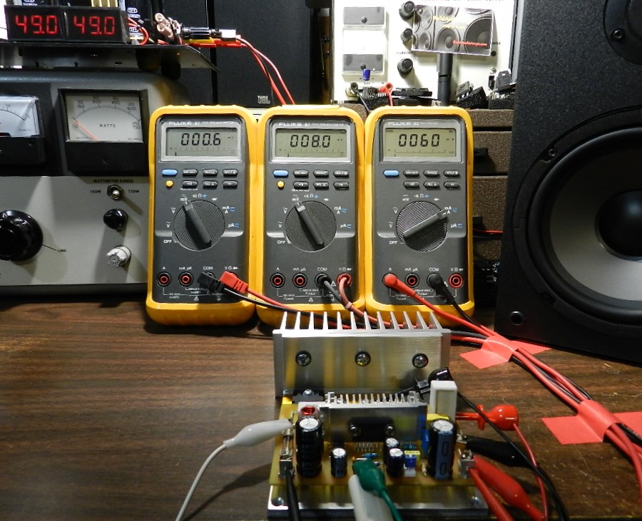
If a Variac transformer is available, connect the AC input of the power supply to the output of the Variac transformer. Switch the power to ON and gradually adjust the Variac’s AC output from zero until the voltage output of the power supply reaches approximately ±49VDC while observing for a sudden increase in any DMM readings. If you have encountered an unusual increase in any of the DMM readings, switch the power to OFF immediately and check the PCB for assembly errors. The picture above shows a DC offset voltage at an amazing 0.6mV. The voltage drop across any emitter power resistor is about 8mV; readjust VR1 to get that DMM reading after 10 minutes of warm-up time. The current across the F+ fuse terminals is 60mA; this value is dependent on the adjustment of VR1 and is adequate. If you obtain similar DMM readings, you may proceed with music test.
If a Variac transformer is unavailable, make sure that the power supply was properly built and that the output voltage rails have been measured at approximately ±49VDC before connecting it to the amplifier project under test. With the power supply switched to OFF, adjust VR1 for maximum resistance. Switch the power supply to ON; the DMM measuring the voltage drop across any emitter power resistor should read less than 1mV. If the DMM reading is more than 1mV and cannot be adjusted by VR1, power OFF immediately and check the PCB for assembly errors. If the DMM reading is less than 1mV, adjust the reading to 8mV after 10 minutes. The DMM that is connected across the F+ fuse terminals will read about 60mA of adequate total current. If you obtain similar DMM readings, you may proceed with music test.
The next test procedure is optional, but if an oscilloscope, audio signal generator and 8Ω dummy load are available, the maximum power output before clipping can be measured. Be careful not to touch the project’s heatsink, it will get very hot during this test.

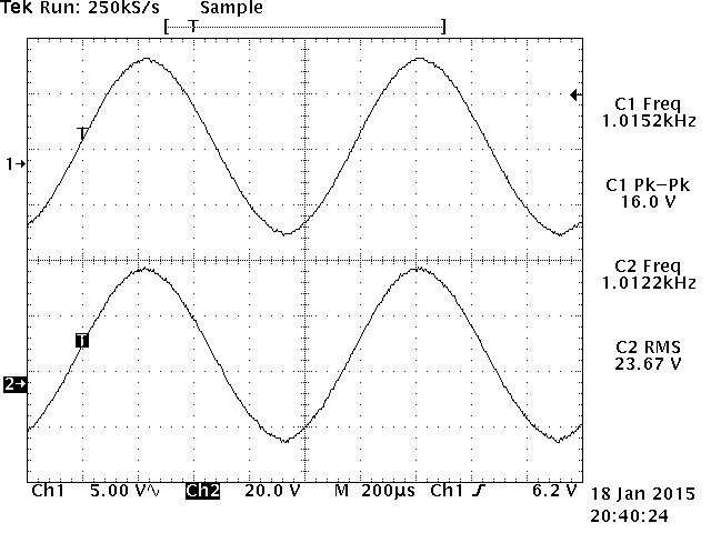
The power output was measured using an HP3312A Function Generator set at 1KHz 16Vp-p sine wave output and connected directly to the input of the amplifier under test as well as the CH1 test probe of the oscilloscope. Notice a high input signal level; obviously the Baker clamp circuit is working and trying to eliminate clipping or artifacts. An 8Ω/700Watt dummy load was connected at the output of the amplifier under test as well as the CH2 test probe of the Tektronix TDS520D 500MHz DPO. The power amplifier produces a very nice sine wave of 23.07Vrms across the 8Ω/700W dummy load or a power output of about 70 Watts, as shown in the TEK hardcopy pictures above. The oscilloscope’s horizontal scale was adjusted at 200uS to verify for any visible clipping or artifacts on either peak. This project was paired with a modified PreAmp1 tone control project; the audio quality reproduced was outstanding.