
Project 12
It was mentioned in Project 8 that future projects will feature the LME49811 as the input stage of different power output stage topologies. As promised, this is one of the many-scaled projects that uses an LME49811 as the input stage of a popular audio amplifier construction kit from the ‘70s called Ampzilla.
The first difficulty of the project is to figure out the right components to substitute the original Ampzilla Parts List. The second challenge is to size the PCB to fit all resistor wattages of the voltage divider that were specified for the circuit design. The third problem is to determine where to connect the source and sink outputs of the LME49811 to the input of Ampzilla’s power output stage.
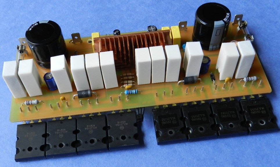
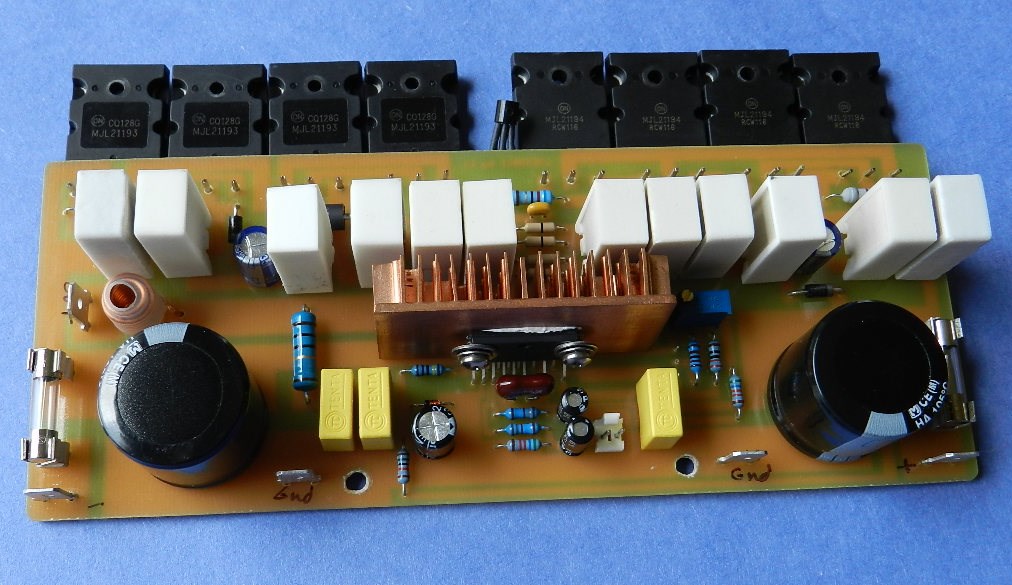
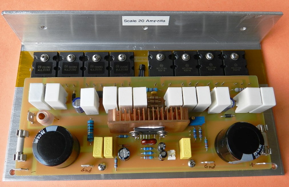
This is what I came up with, populate 4 pairs of T0247 packaged power transistors and use an all 5Watt radial power resistors for the signal voltage dividers on a 2.75” X 7” PCB. The protection circuit was not included in this project. The required power supply at idle is about ±75VDC, but I've decided to power my model unit at ±54VDC, although it was initially tested and auditioned with Project 9 at ±24VDC for hours with splendid musicality.
The power supply requirement, in my opinion, will depend on where you will use the audio amplifier project. If you intend to use it as a sound reinforcement, as in an outdoor sound system, it is preferable to use ±75VDC or even higher. You should also consider adding more power transistors and forced air-cooling into your project. If you intend to use it at home, a ±24VDC to ±54VDC power supply is acceptably good with just enough headroom, but it's entirely up to you!
The PCB layout as well as the Project 12 BOM are provided for free, as is, no warranty.
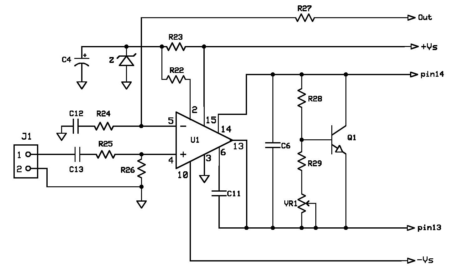
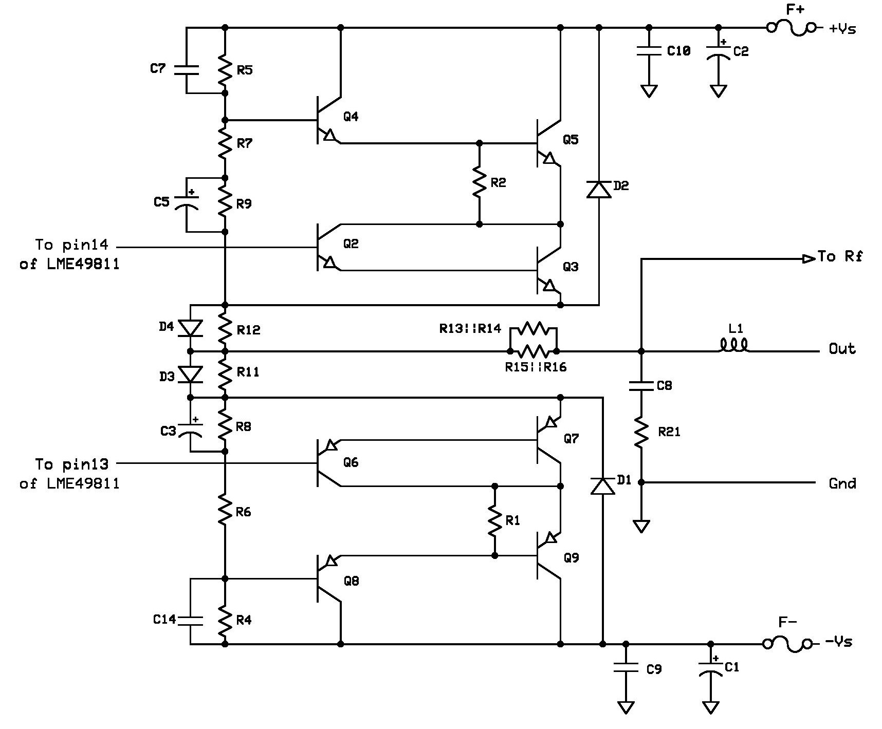
Schematic diagram of the input stage using an LME49811. Schematic diagram of the Ampzilla power output stage.
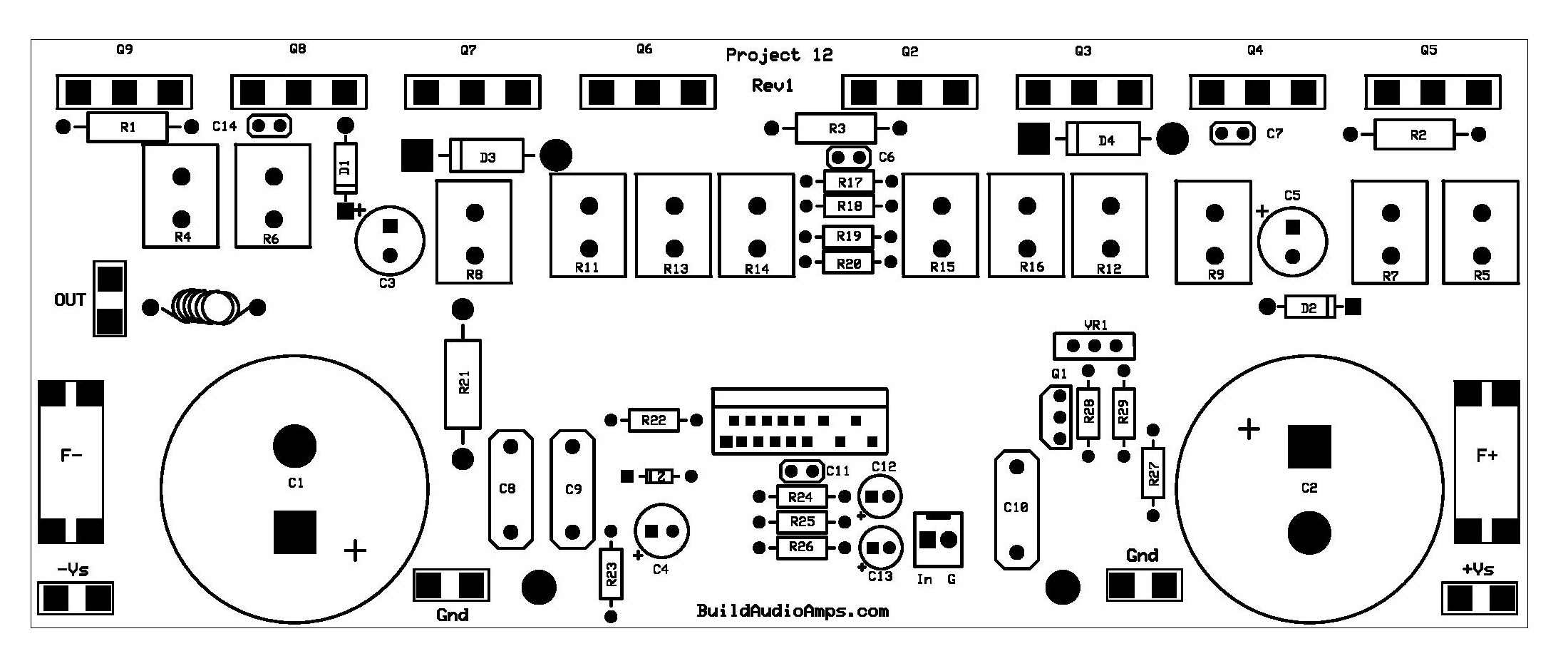 Silkscreen Parts Placement Layer of PCB
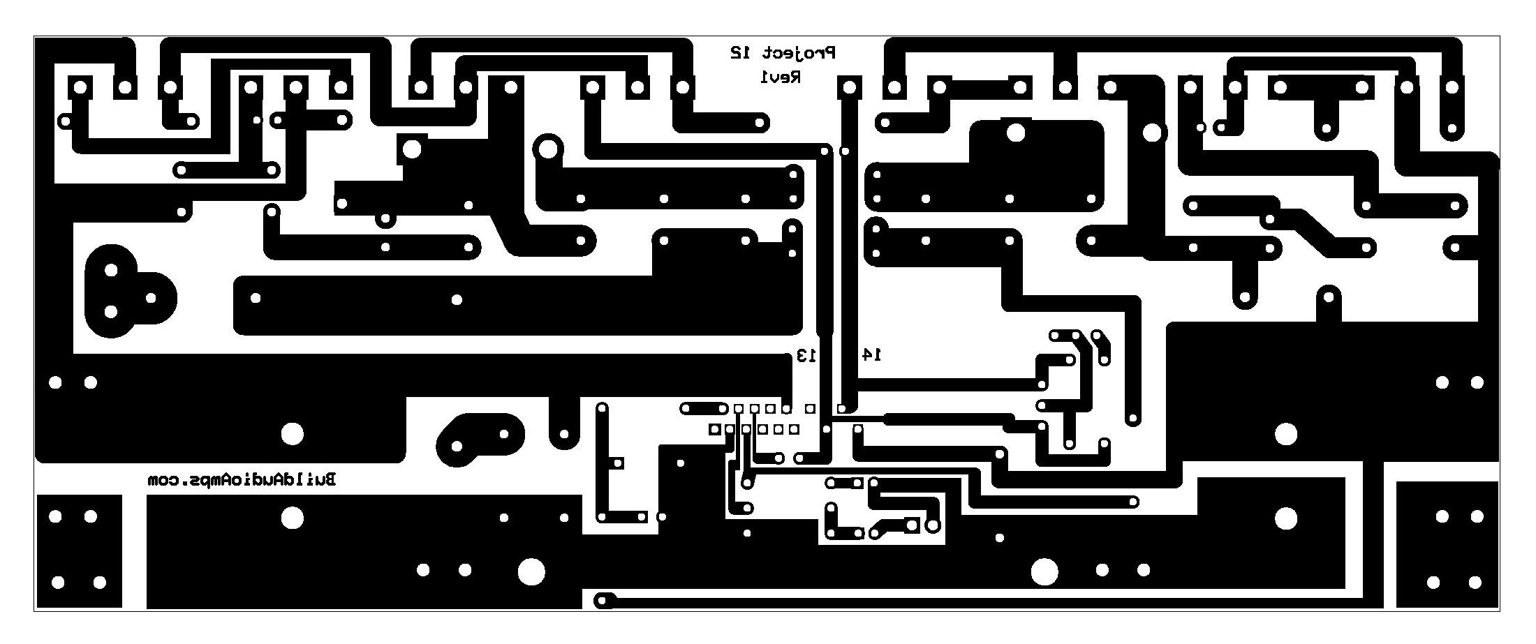
Before listening to any music from your project, let's adjust VR1 first and take some voltage and current measurements.
With the power supply switched to OFF, use an ohmmeter* to read the minimum resistance of VR1 by turning it to fully counterclockwise or until you hear it click. This can be accessed on the top layer of the PCB at the base of Q1 and one end of R29 (please refer to the schematic diagram). Install a jumper or shunt at the input J1. Remove the F+ fuse and insert a milliammeter* at the fuse terminals. Connect a millivoltmeter* at the output and ground pcb terminals.
If you have a ±24VDC power supply use that for initial testing, instead of using a much higher, more unforgiving power supply for the first time.
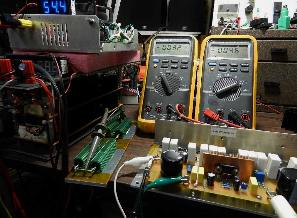
Switch the power supply to ON. With a ±54.4VDC power supply, the millivoltmeter should read about 3mV, the DC offset voltage. The milliammeter connected at the fuse terminals should read about 46mA, as shown in the picture on the left. Other than those readings, power OFF immediately and check for assembly errors.
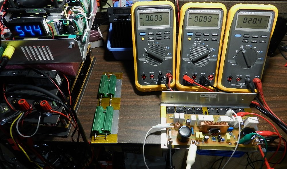
If your project achieved the same DMM readings, that's very good, but before you proceed switch OFF the power supply for now. Connect another millivoltmeter* across D4 to measure the voltage drop at the parallel connected emitter resistor R12. You now have 3 DMMs connected to the amplifier unit under test as shown in the picture on the right. Switch the power supply to ON for a warm-up period of about 30 minutes. Adjust VR1 clockwise to read about 20mV on the millivoltmeter* at D4 . This reading divided by the value of R12 is the idle current of the power output stage according to Ohm's Law. The milliammeter* inserted at the F+ fuse terminals should read about 89mA the total current drawn by the entire circuit. The DC offset voltage, as well as the power supply voltage should stay the same readings as with the previous procedure. Proceed with music test if you successfully completed the above test procedures.
The next procedure is optional. If you have access to a function generator, oscilloscope and 8Ω dummy load, the power output of the amplifier before clipping can be verified. If not, the following pictures will show you just that!

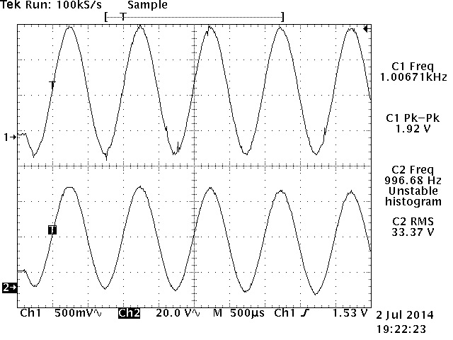
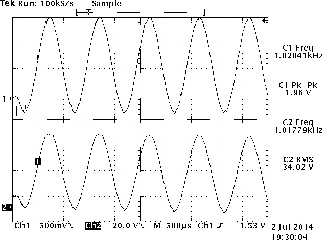
For this procedure a power supply of ±54.4VDC was used by the amplifier under test. A 1KHz 1.92Vpp sine wave input signal was applied into the amplifier, producing an output of 33.37Vrms across the 8Ω load or a power output of about 139Wrms with no sign of clipping. The same 1KHz sine wave signal adjusted to 1.96Vpp produces an output of 34.02Vrms across the 8Ω load or a power output of about 145Wrms with a slight clipping on positive peaks of the waveform as shown in the picture on the right. Enjoy!
*indicates one of the basic functions of DMM.