Project 41
Project 41 showcases Texas Instruments’ LME49830 fully complementary, bipolar, ultra-high fidelity power amplifier input stage driver chip optimized for driving just about any available power MOSFETs. The LME49830 is a high performance driver that features low-noise, very low distortion, thermal shutdown and user adjustable compensation to minimize high-frequency distortion and an optimized slew rate. According to TI, the LME49830 IC can provide possible power output levels in excess of 1kW, if combined with a properly designed high current output stage topology and an adequate thermal management scheme.
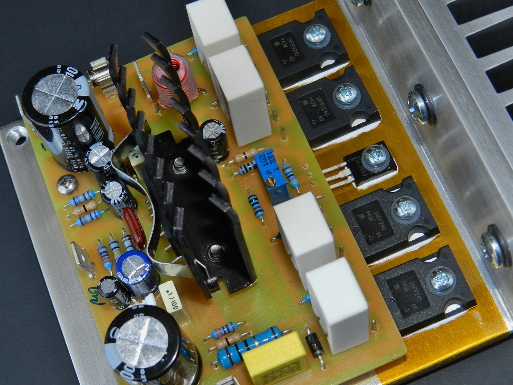
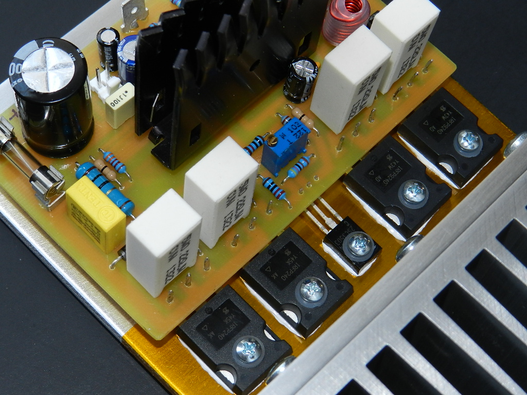
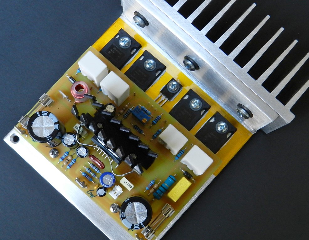
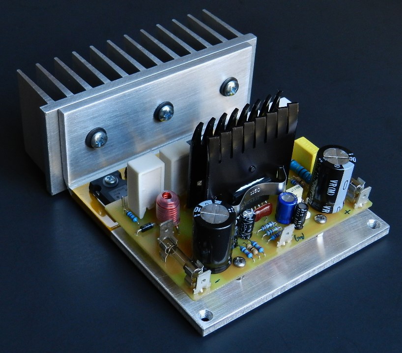
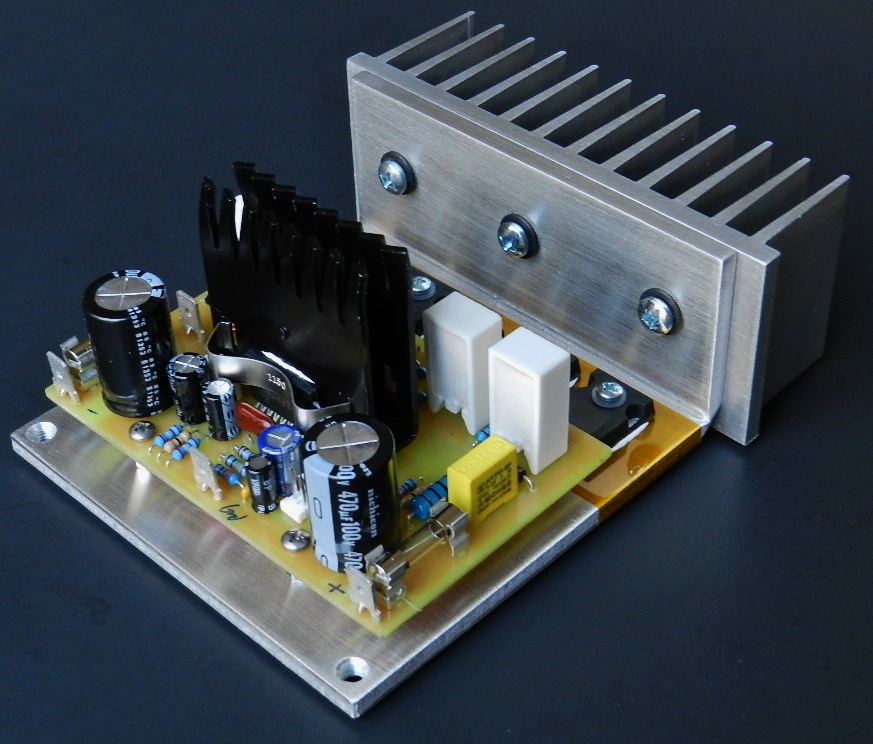
The pilot prototype model has two paralleled MOSFET devices per side in the output stage. There is no power output protection included with this project. However, with the recommended power supply rails and voltage ratings of the power output transistors and the LME49830, there is enough margin of safety. The input sensitivity of the project is about 1.68Vpp resulting in a power output of more than 150 watts with an 8Ω load and ±60VDC to ±72VDC power supply rails with only convection cooling.
Project 41 is configured as a non-inverting amplifier. The gain is set by the value of R4 and R3 at 29.14V/V or 29.3dB. As a builder option, their values can be changed to achieve the desired voltage gain. In actual music listening setup the value of R3, as listed in this project’s BOM, was chosen because of a good high frequency sonic improvement when paralleled with capacitor, Ci. This method of choosing the right values of R3 and Ci is subjective and is something you might want to experiment with, using your favorite speakers.
The LME49830 have two external bias control pins at pins 11 for the negative and 12 for the positive. A thermally compensated VBE multiplier circuit consisting of Q5, VR1, and other associated components is connected into these pins to adjust the bias of the power output devices. With this type of circuit arrangement the bias will remain relatively stable over its temperature operating range. The bias current of about 100mA per transistor was chosen so that crossover distortion is minimized, as shown in the Tek hardcopy picture below, at the same time keeping low quiescent power dissipation level. In an actual power measurement test, VR1 was adjusted so that both peak of the waveform at maximum power output are well rounded just before clipping occurs and then verifying that test results with actual sound quality from a listening perspective. The optimized bias setting was determined at about 22mV across any of the source resistors, R15 thru R18. This is time consuming, subjective and you may experience different results but it’s worth performing.
John L. Linsley Hood published an article entitled “Simple Class A Amplifier” that appeared on the issue of Wireless World in April of 1969, and here’s a portion of the transcript of what he had to say about listening test:
“It would be convenient if the performance of an audio amplifier could be completely specified by frequency response and harmonic distortion characteristics. Unfortunately, it is not possible to simulate under laboratory conditions the complex loads or intricate waveform structures presented to the amplifier when a loudspeaker system is employed to reproduce the everyday sounds of speech and music; so that although the square wave and low-distortion sine wave oscillators, the oscilloscope, and the harmonic distortion analyser are valuable tools in the design of audio circuits, the ultimate test of the final design must be the critical judgment of the listener under the most carefully chosen conditions his facilities and environment allow.”
With that statement, here’s what is considered to be the best part of building this project, the listening test. The prototype unit was connected to a passively modified LM49720 tone control preamp. While playing “Spanish Harlem” by Rebecca Pidgeon from Chesky Records’ Guide to Critical Listening album on a Toshiba HD-A2 player and Kenwood’s quad 12” 3-way speakers, spectacular clarity on the vocals with emphasis on the high frequency, percussion and details on bass was experienced. Playing loudly during Norah Jones’ intro in “One Flight Down” track, from her “Come Away With Me” album reproduced the same musical fidelity experience. The entirety of Massive Attack’s “Collected” album was also auditioned with the same setup for endurance music testing.
If you are interested in building this project and have read the Information and Policies section of this website, the schematic diagram, PCB layout (available only by request) and BOM are free, as is, no warranty.
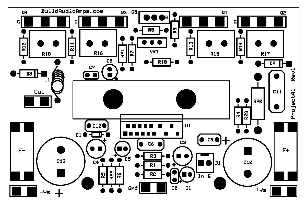
Project 41 Silkscreen Parts Placement Layer of PCB.
If you’ve decided to build this project, the idle current needs to be adjusted first before going any further. Insert a jumper or shunt at the input of the amplifier. Do not connect any load or loudspeaker at the output of the amplifier. Adjust VR1 for maximum resistance of 1KΩ; please refer to the schematic diagram where to access VR1 on top of PCB. Prepare 3 DMMs to measure the DC offset voltage at the output of the amplifier, the voltage drop of the source resistor in any of the power output transistors, Q1 through Q4 and the overall current across the F+ fuse terminals. It is highly recommended to use a Variac transformer when performing the initial test of the project. If something goes wrong with the project, minimal damage will occur to the components or just a blown fuse. However both test procedures with or without the use of a Variac transformer will be explained.
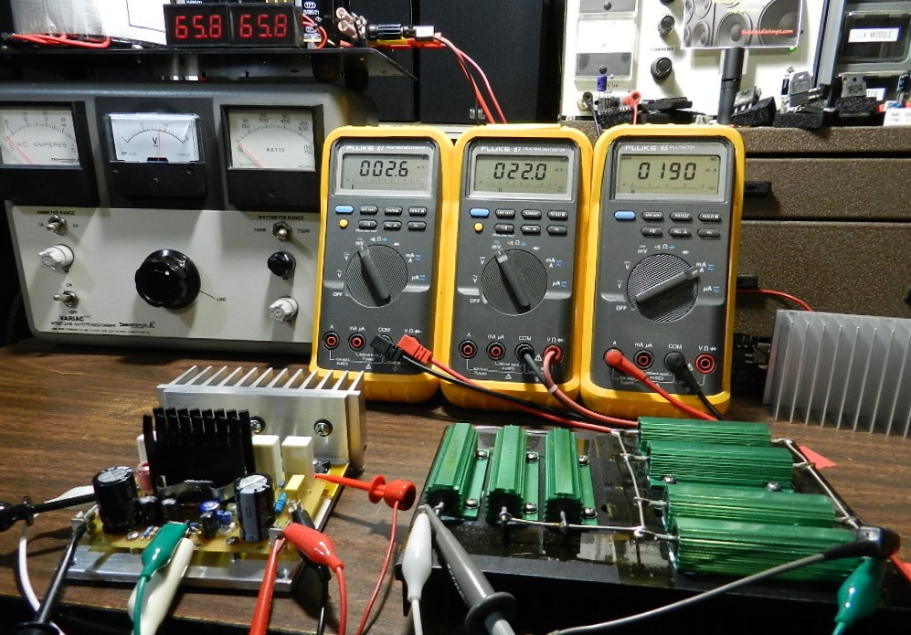
If a Variac transformer is available, connect the AC input of the power supply to the output of the Variac transformer. Switch the power to ON and gradually adjust the Variac’s AC output from zero until the voltage output of the power supply reaches approximately ±65VDC while observing for sudden increase in any DMM readings. If you have encountered an unusual increase in any of the DMM readings, switch the power to OFF immediately and check the PCB for assembly errors. The picture above shows a DC offset voltage at 2.6mV. The voltage drop across any emitter power resistor is about 22mV; readjust VR1 to get that DMM reading after 10 minutes of warm-up time. The current across the F+ fuse terminals is 190mA; this value is dependent on the adjustment of VR1. If you obtain similar DMM readings, you may proceed with music test.
If a Variac transformer is unavailable, make sure that the power supply was properly built and that the output voltage rails have been measured at approximately ±65VDC before connecting it to the amplifier project under test. With the power supply switched to OFF, adjust VR1 for maximum resistance. Switch the power supply to ON; the DMM measuring the voltage drop across any source resistor should read less than 1mV. If the DMM reading is more than 1mV and cannot be adjusted by VR1, power OFF immediately and check the PCB for assembly errors. If the DMM reading is less than 1mV, adjust the reading to approximately 22mV after 10 minutes or more. The DMM that is connected across the F+ fuse terminals will read about 190mA of total current. If you obtain similar DMM readings, you may proceed with music test.
After adjusting the bias for either test procedures, let the prototype unit completely cool down at ambient temperature. Then reapply power to the unit under test; the voltage drop across any source resistor should be more than 40mV while the total current should be more than 300mA. This will eventually go down and stabilize to their original adjusted set values.
The next test procedure is optional, but if an oscilloscope, audio signal generator and 8Ω dummy load are available, the maximum power output before clipping can be measured. Be careful not to touch the project’s heatsink and dummy load, both will get very hot during this test.

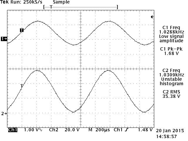
The power output was measured using an HP3312A Function Generator set at 1KHz 1.68Vp-p sine wave output and connected directly to the input of the amplifier under test as well as the CH1 test probe of the oscilloscope. An 8Ω/700Watt dummy load was connected at the output of the amplifier under test as well as the CH2 test probe of the Tektronix TDS520D 500MHz DPO. The power amplifier produces a very nice sine wave of 35.38Vrms across the 8Ω/700W dummy load or a power output of more than 150 watts, as shown in the TEK hardcopy pictures above. The oscilloscope’s horizontal scale was adjusted at 200uS to verify for any visible clipping or artifacts on either peak. Enjoy!