
Project 3
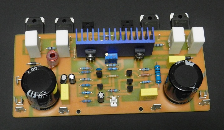
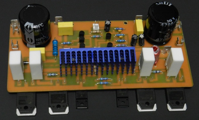
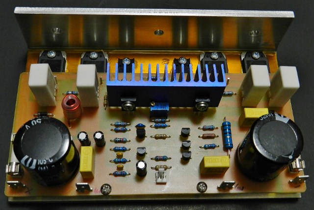
You may call Project 3 as another simple audio amplifier circuit but the audio quality is surprisingly good. The model unit was built with what's available in The Parts Bin: 2 pairs of 2SC5242 and 2SA1962. 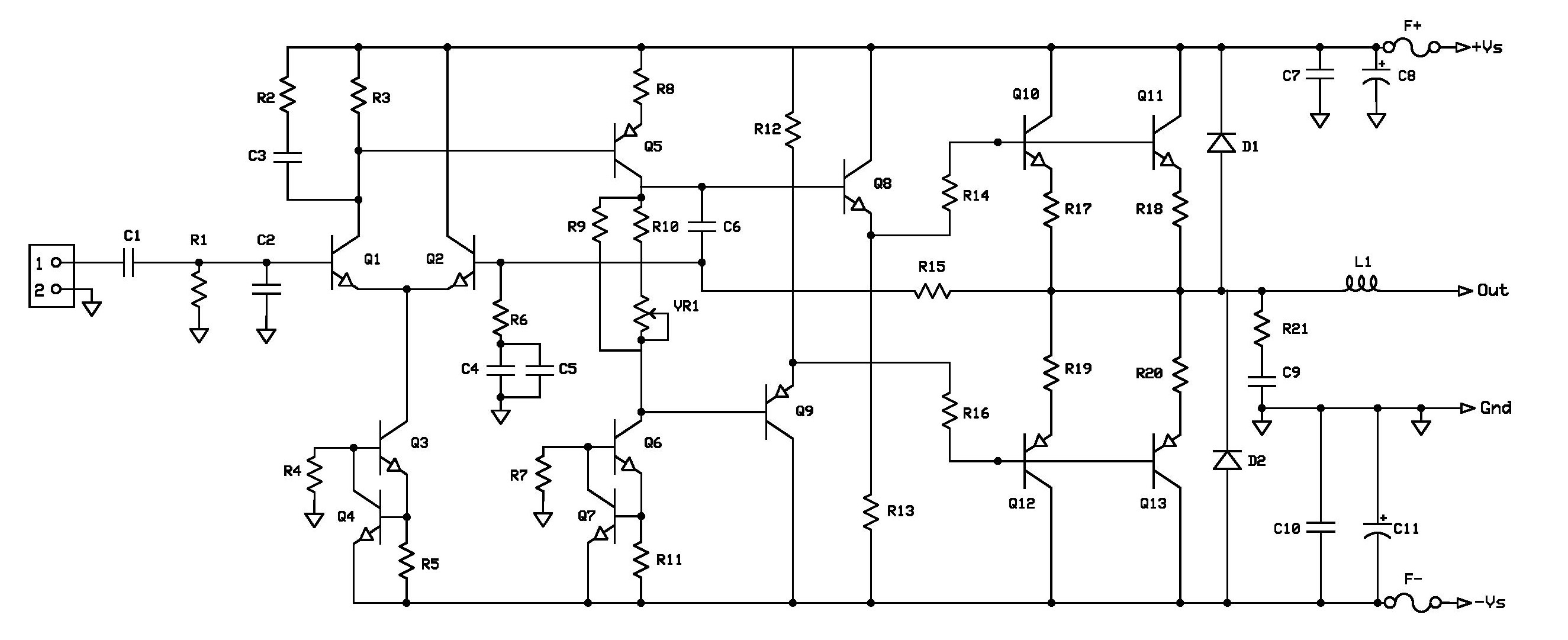
Schematic Diagram of Project 3
Here's a brief descripion of the circuit:
The amplifier uses 2 identical constant current-source circuits, Q3/Q4 and Q6/Q7. The input differential amplifier Q1/Q2 uses the first current-source circuit while Q5 uses the second current-source circuit. Q5 is a Class A voltage amplifier stage, frequency compensated by C6. Q5’s output drives the emitter-follower Q8 and Q9, whose emitter resistors are connected to the supply rails instead at the output. Q8 and Q9 accordingly drives the complementary push pull parallel power output transistors Q10 thru Q13 and are protected by clamping diodes D1 and D2. R21, C9 and L1 at the output are necessary for stability of the amplifier at any loads. There should be a resistor in parallel with L1, you can populate a 4.7Ω 2W resistor SMT type at the bottom copper layer of the PCB. The idle current adjustment is passively done by VR1. The overall gain of the amplifier is detemined by the ratio of feedback resistor, R15 and R6 in series with C4 and C5. Transistors Q8 thru Q13 does not require a large heatsink, the thick aluminum-mounting bracket was sufficient enough.
Now if you decide to build Project3, then put together the printed circuit assembly (PCA), i.e. create and populate the PCB. A PCB layout and Bill Of Materials (Project3 BOM) are provided for free, as is, no warranty.
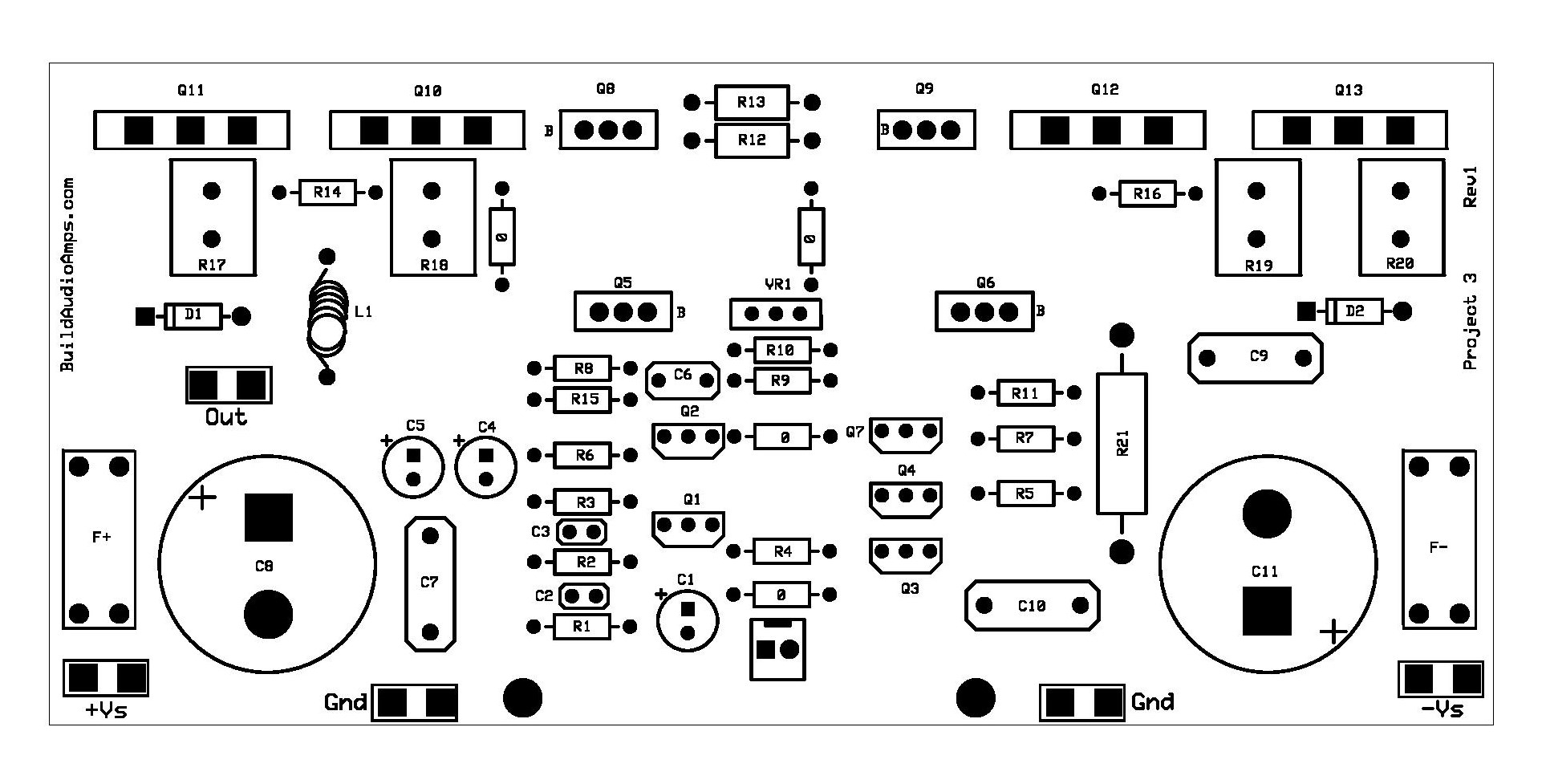
Silkscreen Parts Placement Layer of PCB
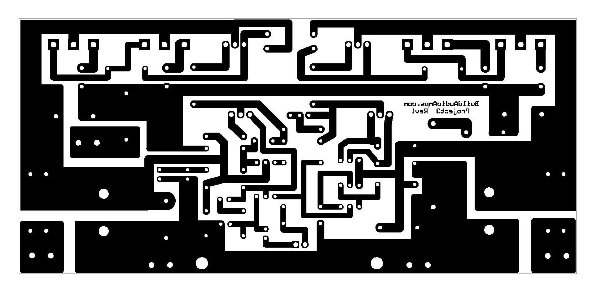
Bottom Copper Layer of PCB
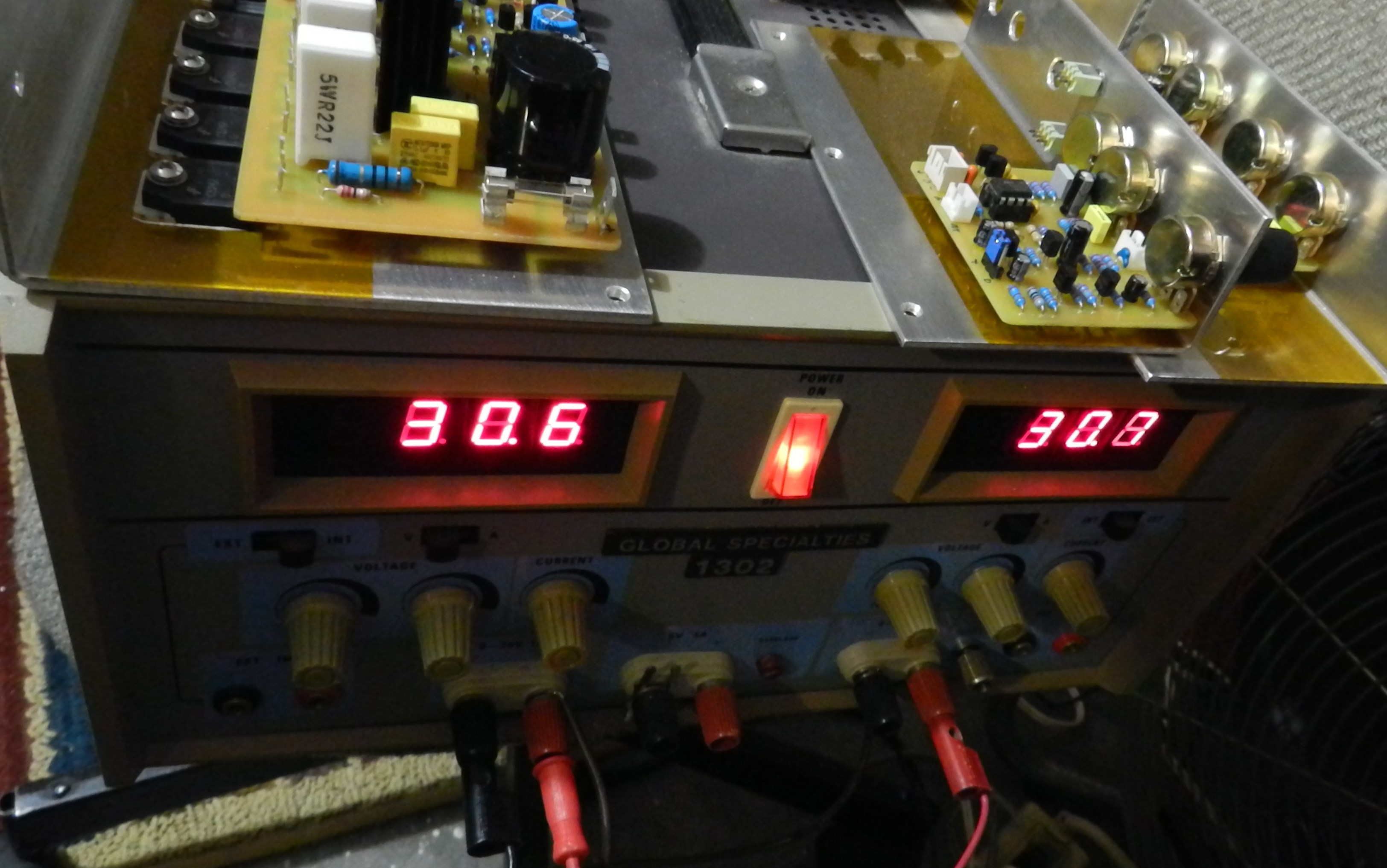
Here comes the fun part of the project once assembly is complete. Visually inspect the PCB for component orientation or polarity, trace shorts, cold solder and so forth. Connect an ohmmeter* at the collector of Q6 and one end of R10. Adjust VR1 to read about 0Ω across its terminals. I will be using a ±30VDC power supply to test this project, but the main power supply rails of the amplifier can go up to ±35VDC with no problems.
With the power OFF, remove F+ fuse and insert a milliammeter* at the fuse terminals. Do not connect a load or speaker at the output, instead connect a millivoltmeter* to measure the DC offset voltage. Switch the power supply to ON. If you think you did a good job, the millivoltmeter* connected at amplifier’s output will read about 32mV, and the milliammeter* at the F+ fuse terminals will read some current in the mA range. The voltmeters* connected at the power supply should read whatever voltage you apply to the amplifier under test and should not change. Switch the power supply to OFF.
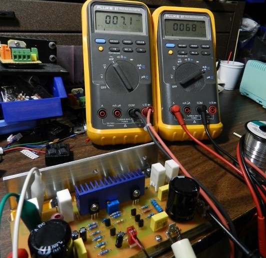
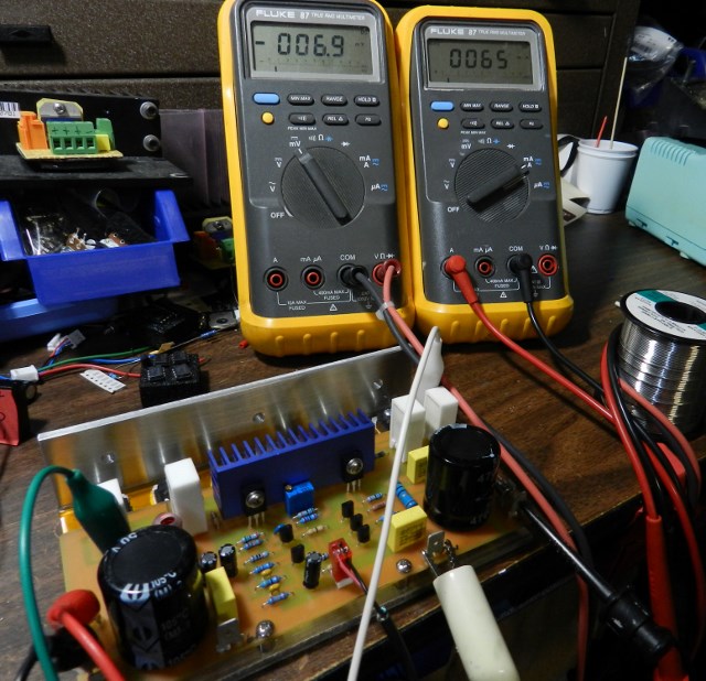
Disconnect the millivoltmeter* from the output of the amplifier and connect that to the emitter of Q11 and output pcb terminal. Switch power supply to ON. Adjust VR1 counterclockwise to get about 7mV. The picture on the left shows a 7.1mV reading, the white test clip is connected to the emitter of Q11 and the green test clip is connected to the output pcb terminal. The picture on the right shows a -6.9mV reading, notice the white test clip has been moved to the emitter of Q13. The DMM on the right side of both pictures is reading the current at the F+ fuse terminals at about 65 to 68mA.
If your project behaved differently from what have been described, power OFF immediately. Check for cold or bridge solder, component orientation and etc. After you’ve discovered your mistake, repeat the same test procedures. Readjust VR1 after a warm-up period of about 30 minutes. Finally it is time for music test, connect your test speaker and favorite music source and enjoy!
* refers to one of the basic functions of a DMM.