Project 49


Project 49 is another fully symmetrical complementary Current Feedback Amplifier project. The prototype model of this project achieved a power output of 216 watts at 8Ω with ±64VDC power supply rails. However, higher power output is possible with 4Ω loads. The wide bandwidth characteristic of a CFA-based audio power amplifier resulted in a slew rate of 153V/uS. The actual measured waveform will be shown later. The sonic performance during music test also reveals the spectacular attribute of a CFA-based audio power amplifier.
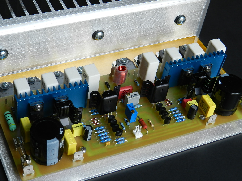
Please refer to the project’s schematic diagram for a brief description of the circuit. The input signal at J1 is directly coupled and passes through a low pass filter consisting of R1 and C1 that suppresses unwanted RF noise from entering the complementary emitter-follower buffer stage transistors, Q1 and Q2. R2 supplies the necessary base bias for Q1 and Q2 and its chosen value also reduces the overall DC offset voltage of the amplifier to minimum. The output of the buffers drives the summing stage transistors, Q4 and Q5. A feedback node consisting of R12 and R13 in parallel with VR1 sets the overall DC offset voltage of the amplifier by ±100mV. If optimum DC offset voltage is desired, an integrator op-amp similar to the one used in Project 4 can be implemented. However, there’s an improvement to the DC offset settling time in this project compared to previous CFA-based projects because of the additional cascode transistors to the error amplifier transistors. Negative feedback resistors, R15, and R26, are also connected in that same feedback node. These resistors determine the overall gain of the amplifier at about 26dB. If you’re interested in altering the gain of this project, here’s an "Application Report SLOA105A from Texas Instruments" on calculating the gain of an audio amplifier.
The outputs of Q3 and Q6 are connected to another cascode arrangement of Q7/Q8 and Q11/Q10. These allow better isolation of the outputs of the input stages from the pre-driver stages, improves actual measured slew rate and differentiate this project from earlier CFA-based projects. A VBE circuit consisting of Q9, VR2 and other associated components sets the bias requirement of the output stage transistors. A frequency compensation capacitor, C4, is connected at the emitter of Q9 to signal ground.
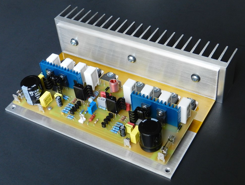
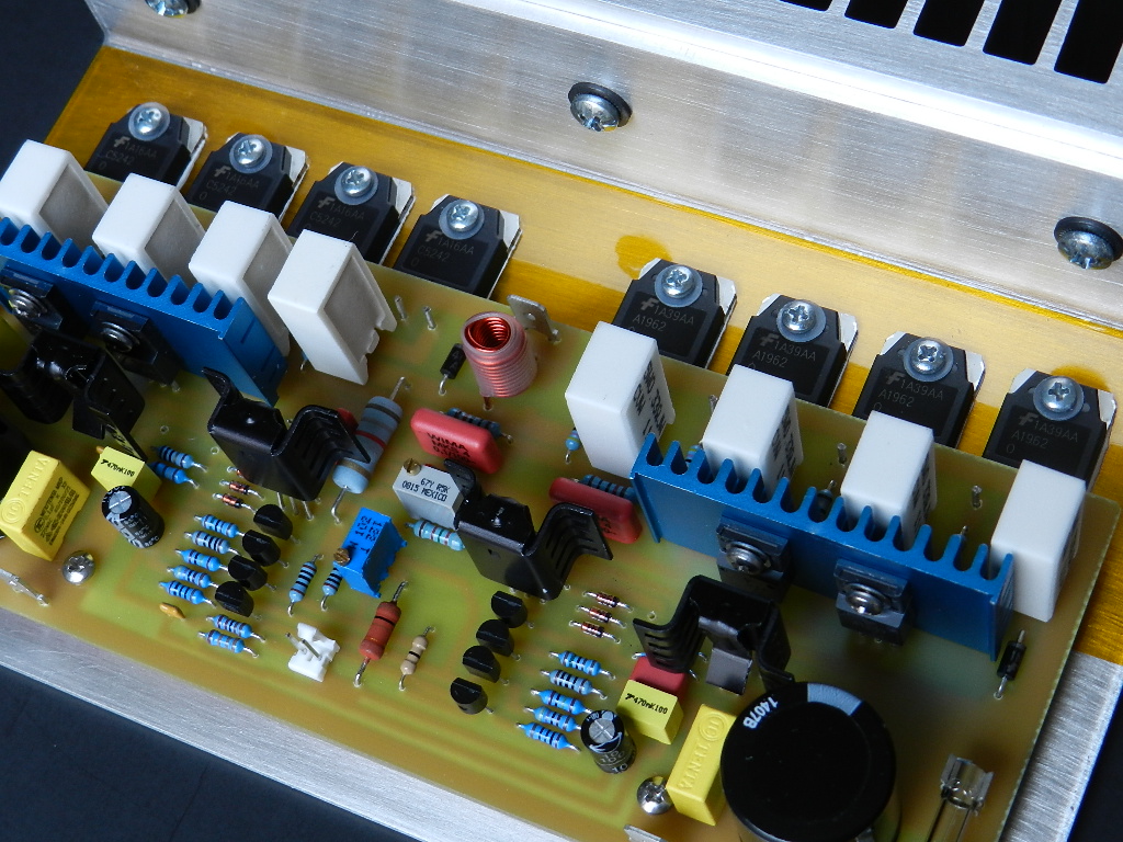
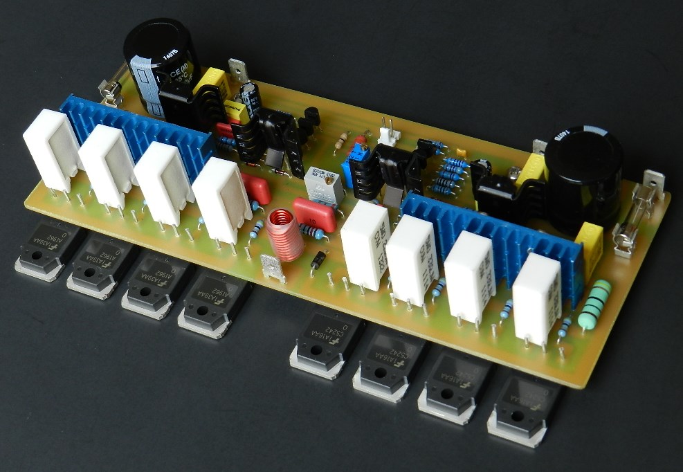
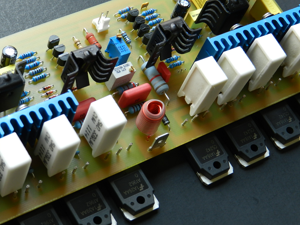
The output stage consists of a modified triple emitter-follower configuration that improves isolation between paralleled power output transistors. A complementary pair of T0-126 packaged pre-driver transistors, Q12 and Q13, isolates the output of Q8 and Q10 from the paralleled complementary T0-220 packaged driver transistors, Q14//Q15 and Q16//Q17. Q12 and Q13 are frequency compensated by C6 and C7. Here’s the kicker: the output of Q14 drives two paralleled TO3P-packaged NPN power output transistors, while Q15 drives another paralleled TO3P-packaged NPN power output transistors. The output of Q15 drives two paralleled TO3P-packaged PNP power output transistors, while Q17 drives another paralleled pair of TO3P-packaged PNP power output transistors.
This type of power output stage configuration may be implemented for high performance high-powered audio amplifier applications. Instead of two paralleled power output transistors per T0-220 driver transistor, as utilized in this project, four or more power output transistors may be paralleled per T0-220 driver transistor. As a result of adding more power output devices, the power supply rails can now safely be increased thus increasing also the power output of the amplifier.
There’s no protection circuit that’s included in the prototype, however, the “uPC1237 Speaker Protection and Power ON Delay Project”, may be implemented to this project for peace of mind. A simpler alternative is to use a 10-amp fuse in series with the main amplifier output and speaker. Hopefully, this will protect the power output transistors from damage in case of accidental speaker cable shorts.
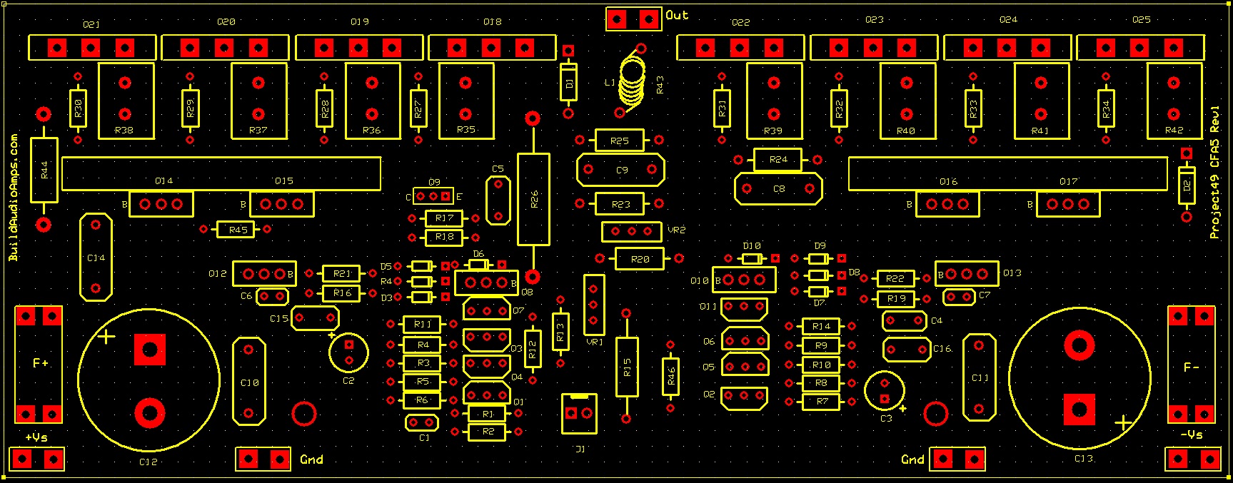
Project 49 Silkscreen Parts Placement Layer of PCB.
The prototype model was built on a 7.75” X 3.0” single-sided PCB. All components used in the prototype model are readily available standard parts. If you are interested in building this project and have read the Information and Policies section of this website, the schematic diagram, PCB layout (available only by request) and BOM are free, as is, no warranty.
Be sure to measure the very high resistance ohmmeter reading (greater than 1MΩ to ∞) between collectors of all power output transistors and the aluminum mounting bracket/heatsink. A small leakage resistance would affect the overall sonic performance of the amplifier. Also apply a generous amount of heatsink compound to these power transistors.
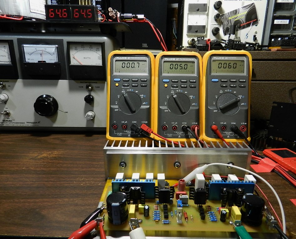
The amplifier requires approximately ±64VDC power supply rails. These rails are produced from a rectified and filtered 90VCT at approximately 300VA toroidal power transformer. The picture above shows a panel voltmeter reading at about ±64VDC, obtained by connecting the AC input of the power supply to the AC output of a Variac transformer. Gradually adjust the Variac transformer so that the panel voltmeter reads from 0V to about ±65VDC while observing the DMMs: connected at the output of the amplifier, across the emitter resistors, R38 and R42 and the overall current at F+ fuse terminals. Power off immediately if you have noticed a higher DMM reading other than what’s shown in the picture above. Check the PCB for any assembly errors.
Allow the amplifier to warm-up for at least 15 minutes or more, before making any adjustments to VR1 and VR2. The DMM on the left side of the picture is measuring the DC offset voltage at 0.7mV, which can be set as close to 0mV as possible by VR1. The DMM in the middle measures 5mV across the power output transistor’s emitter resistors, R38 and R42, or between the emitters of Q21 and Q25. This measurement can be acquired by adjusting VR2 and could be anywhere from 5mV to 25mV depending on the builder. The DMM on the right side of the picture is measuring the overall current across the F+ fuse terminals at 60mA and is dependent on the adjustment of VR2.
Surprisingly, adjusting the bias at 5mV or 15mA, there’s no perceivable audio distortion experienced during listening test, even at very low input signal level, like in a classical Adagio music. As a result the heatsink in the prototype is sufficient enough to cool the amplifier for extended period of normal listening conditions.
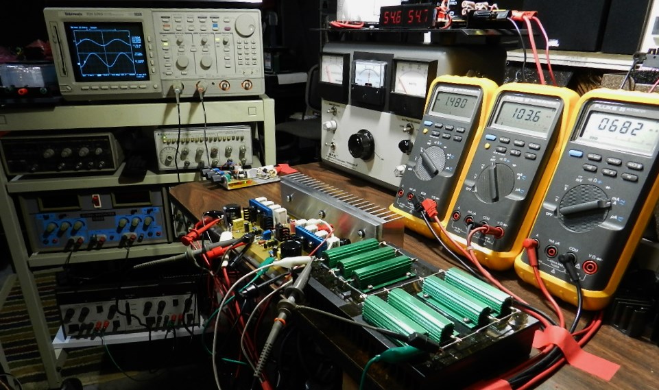
The picture above shows the test setup for power output and slew rate measurements. An HP3312A function generator and a Tektronix TDS520D 500MHz oscilloscope was used for these particular tests. However, similar equipment can be used if you’re planning to perform the same optional tests. Be careful not to touch the amplifier under test, heatsink and dummy load; they will get hot.
The dummy load is only connected to the amplifier during power output measurement. It should be disconnected from the output of the amplifier during slew rate measurement. The Zobel network resistor R44, a 10Ω 3W wire wound power resistor, should be disconnected as well. Running a continuous 100KHz square wave signal to the amplifier will destroy this resistor.
The measured power output of the amplifier before clipping is 216watts at 8Ω or about 433 watts at 4Ω load with ±64VDC power supply rails. This power output was achieved by applying a 5.8Vpp 1KHz sine wave signal to the input of the amplifier that resulted to an output signal of 41.5Vrms across an 8Ω dummy load, as shown on the left below. The slew rate measurement output waveform is shown on the right below. This was obtained by applying the input of the amplifier with a 100KHz square wave signal and the amplitude was adjusted so that the output waveform does not show any overshoots on its peaks, which is about 49.6Vpp. This corresponds to a slew rate of about 153V/uS.
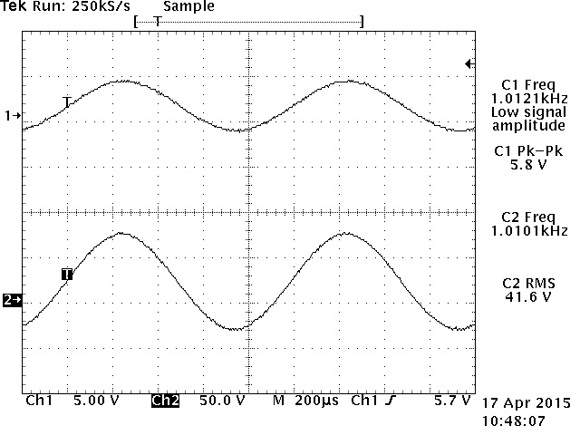
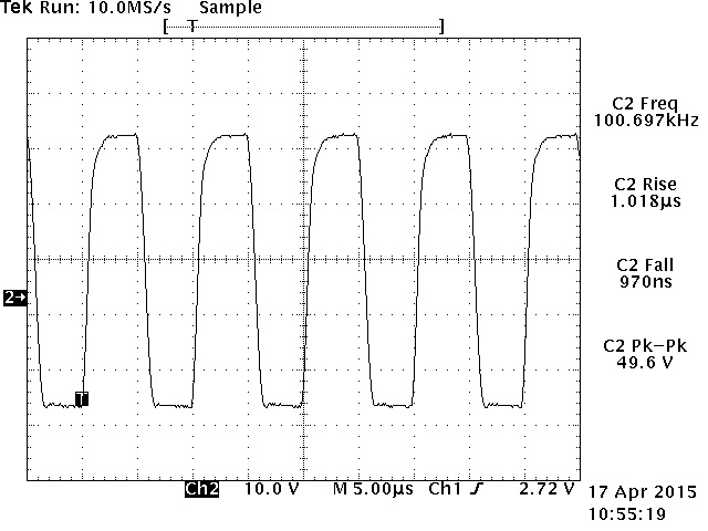
Power output measurement waveform. Slew rate measurement waveform.
“Perhaps more than any other discipline, audio engineering involves not only purely objective characterization but also subjective interpretations. It is the listening experience, that personal and most private sensation, which is the intended result of our labors in audio engineering. No technical measurement, however glorified with mathematics, can escape that fact” – Richard C. Heyser
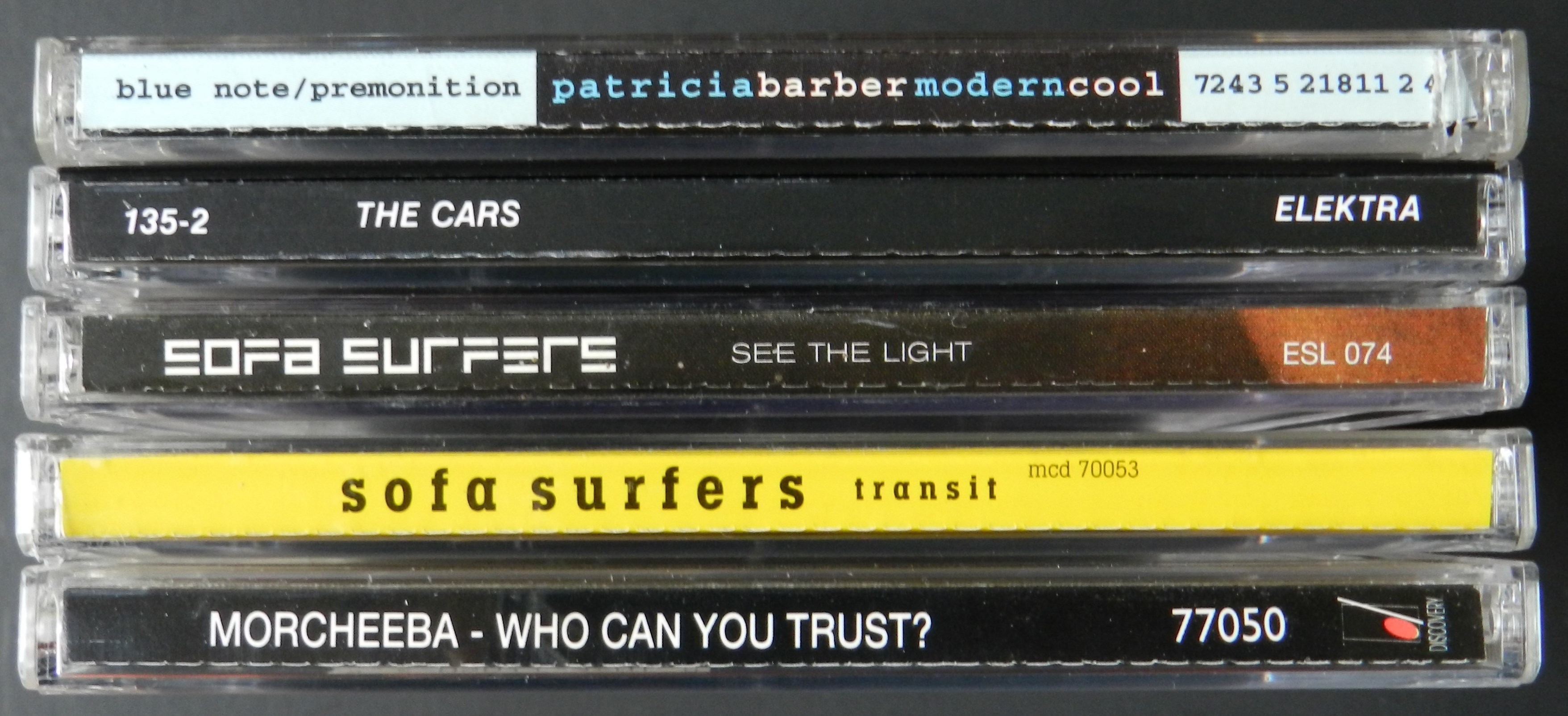
In real world listening with various music materials, the experience was extraordinary. The prototype unit was connected to a modified LM49720 tone control preamp. Listening to Patricia Barber’s version of “Light My Fire” from her “Modern Cool” album, played on a Toshiba HD-A2 player and a Kenwood MV-9D monitor speaker, you hear impressive clarity of the audio frequency spectrum. An HDCD version of The Cars debut album was also played with very good musical fidelity. The entirety of Sofa Surfer’s “See the Light” CD album was also played for endurance testing. Other CD albums shown above were also auditioned as well during listening test.