Project 26
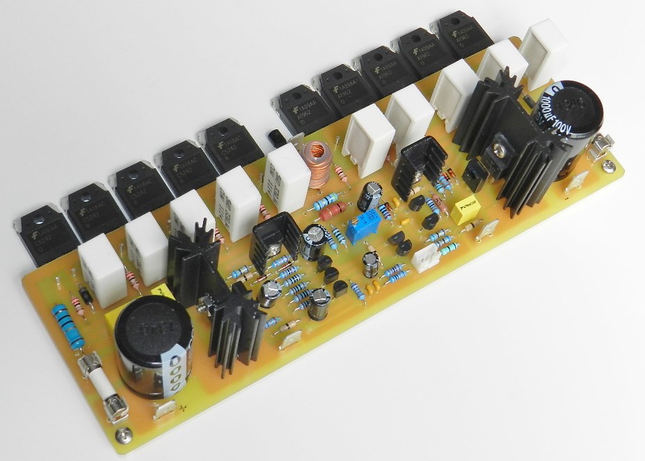
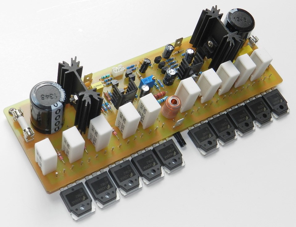
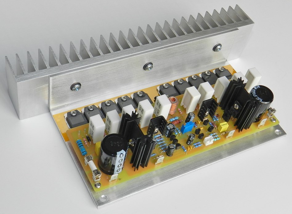
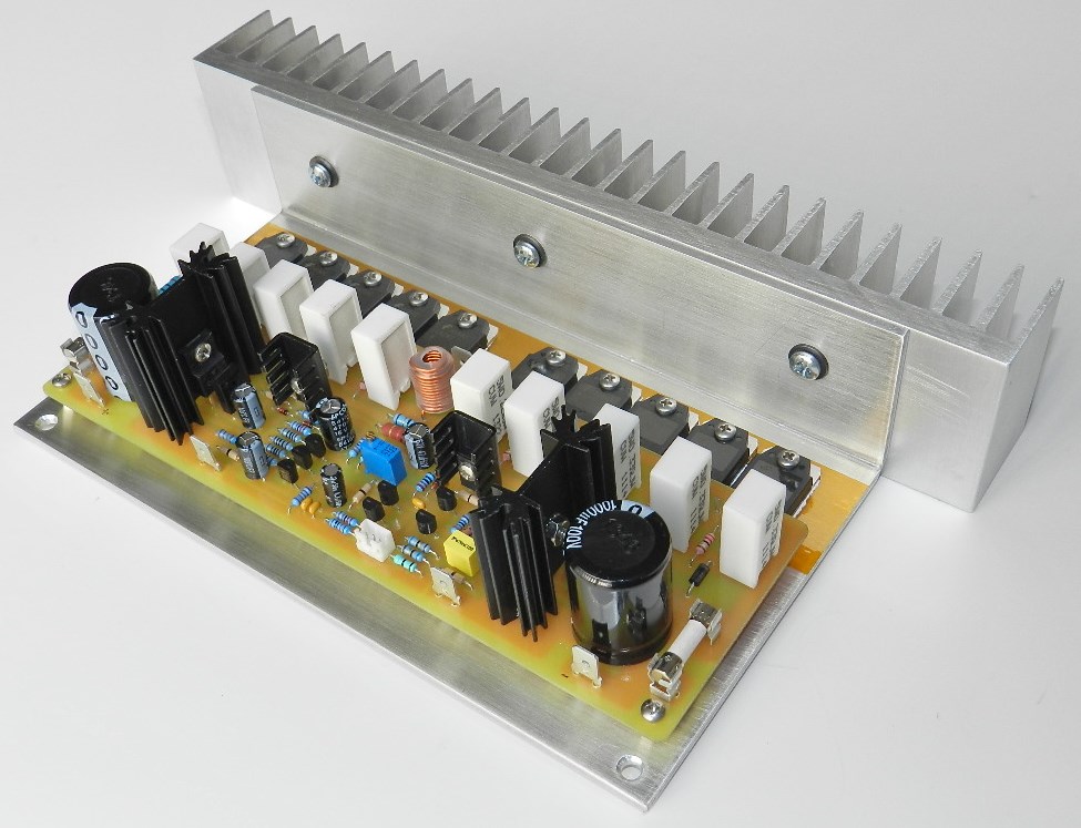
Project 26 is a conventional power amplifier that uses a triple emitter-follower output stage. The measured power output of Project 26 is 238Wrms into an 8Ω load with a ±64VDC to ±70VDC power supply rails. Here’s a brief description of the project’s circuit:
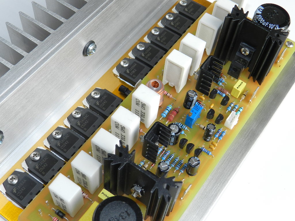
The input signal at J1 passes through a low pass filter circuit, which removes unwanted radio frequency signals from entering the base of Q1. Notice the low resistance value of Rb for Q1 and the negative feedback resistor R10. Q1 and Q2 form an input differential amplifier stage, current-sourced by Q3 and their collectors loaded by current-mirror transistors, Q4 and Q5.
The output of Q1 is connected to an emitter follower, Q7, which buffers the signal from the voltage amplifier stage, Q10. Q10 is loaded with a current-source D1, D2 and Q8. The voltage amplifier stage is high frequency compensated by C7 and C8 in parallel with D3. The Vbe multiplier transistor, Q9, is populated off the PCB and mounted close to the power transistors, along with VR1, which set the bias adjustment for the power output transistors. The power output stage is a triple emitter-follower topology. The first emitter-follower stage consists of Q11 and Q12 in TO-126 packaged transistors with shared emitter resistor, R21. This stage buffers the output of Q10 to the next stage and provides some current gain. The second emitter-follower stage consists of Q13 and Q14 comes in TO220 package, again uses a common shared emitter resistor, R22. The third emitter-follower stage consists of five pairs of paralleled complementary 17A/250V/130W TO3P packaged power output transistors that provides large amount of current to drive an 8Ω or a 4Ω load.
The combination of L1 in parallel with R44 and R43 in series with C12 connected at the output, assures the amplifier’s stability when connected to any loads. The gain of the amplifier is determined by the ratio R10 and R11 in series with C6. All front-end TO-92 packaged complementary transistors used for this project are rated at 300V/0.5A/625mW from Fairchild Semiconductors.
If you’re interested to build this project and have read the Information and Policies section of this website, the schematic diagram, PCB layout (by request) and BOM are available for free, as is, no warranty.
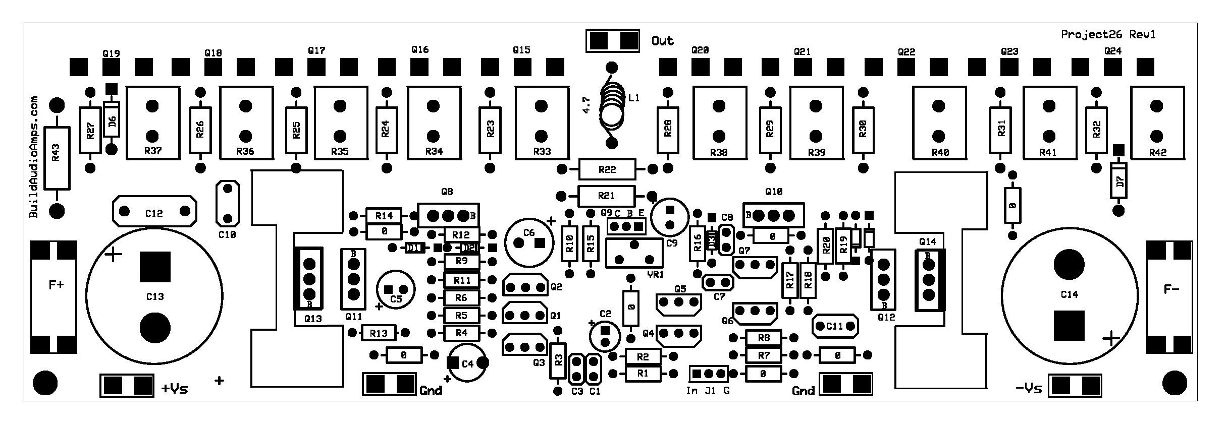 Project 26 Silkscreen parts placement layer of PCB.
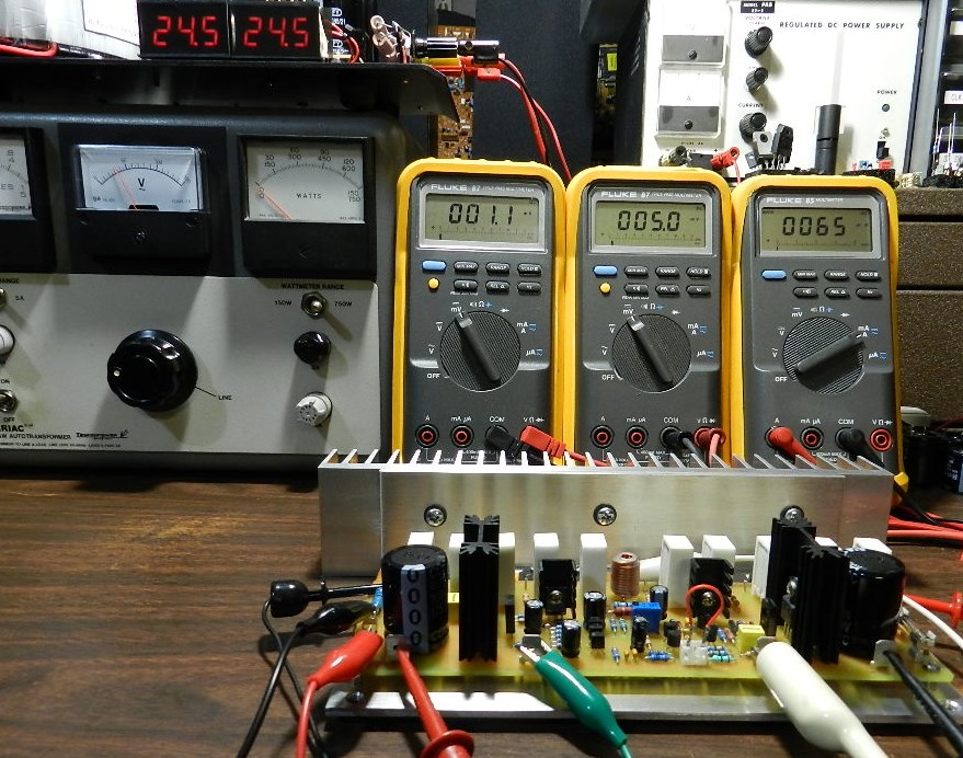
A safe way of powering up your newly built project the very first time is to use a ±24VDC power supply or whatever low-voltage dual-polarity power supply that you may have. Doing so will eliminate most of the disappointment involved when the unexpected happens to the project powered with high power supply voltage rails. Like in most previous projects, I’ve always used a ±24VDC power supply to initially power the amplifier for testing.
Insert a piece of jumper wire at the input of the amplifier. Do not connect any load or loudspeaker at the output of the amplifier. Prepare 3 DMMs to measure the DC offset voltage, the voltage between the emitters of Q19 and Q24 power output transistors and the current across the F+ fuse terminals. Seasoned amp builders have more than three DMMs.
The picture on the left with a ±24VDC power supply shows the DC offset voltage at 1.1mV measured at the output of the amplifier, 5mV across the emitters of Q19 and Q24 and the current measured across the F+ fuse terminals at 65mA. Carefully adjust VR1 to obtain the 5mV reading after a warm-up period of about 10 minutes. If you get different DMM readings, switch the power supply to OFF immediately and check the PCB for assembly errors. If you intend to power the project at this voltage level you may do so, the music fidelity it reproduced, in my opinion, is still very pleasing and does not disappoint! If not, you may proceed with the next test.
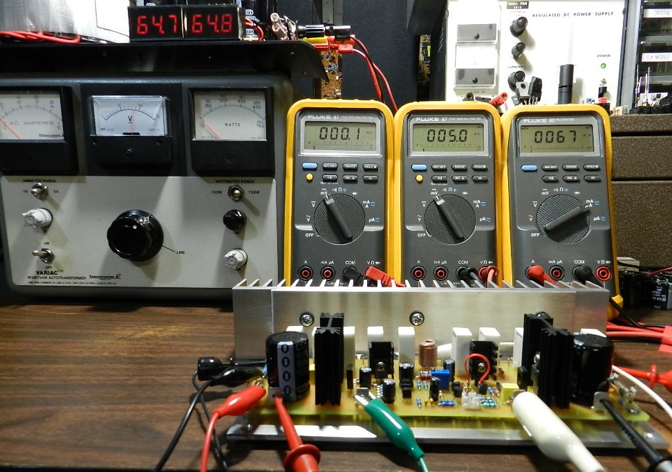
If a Variac transformer is available, connect the AC input of the power supply to the output of the Variac transformer. Switch the power to ON and gradually adjust the Variac’s AC output voltage from zero until the voltage output of the power supply reaches ±64VDC while keeping an eye on sudden increase in any DMM readings. If you have observed an increase in any of the DMM readings, try adjusting VR1 if it decreases that specific DMM reading, if not switch the power to OFF immediately and check the PCB for assembly errors. The picture on the right with a ±64VDC power supply shows a DC offset voltage at 0.1mV, the voltage across Q19 and Q24 at 5mV and the current across the F+ fuse terminals at 67mA. Readjust VR1 to get the 5mV reading after 10 minutes, after that, you may proceed with music test, the test that you’ve been waiting for!
If a Variac transformer is unavailable, make sure that the power supply has been properly built and that the output voltage rails have been measured at ±64VDC before connecting it to the project. With the power supply at OFF, adjust VR1 for minimum resistance. Switch the power supply to ON; the DMM measuring the voltage across Q19 and Q24 should read less than 1mV. If the DMM reading is more than 1mV and cannot be adjusted, power OFF immediately and check the PCB for assembly errors. If the DMM reading is less than 1mV wait for 10 minutes for the bias to stabilize and then carefully adjust the reading to 5mV, after that, you may proceed with music test!
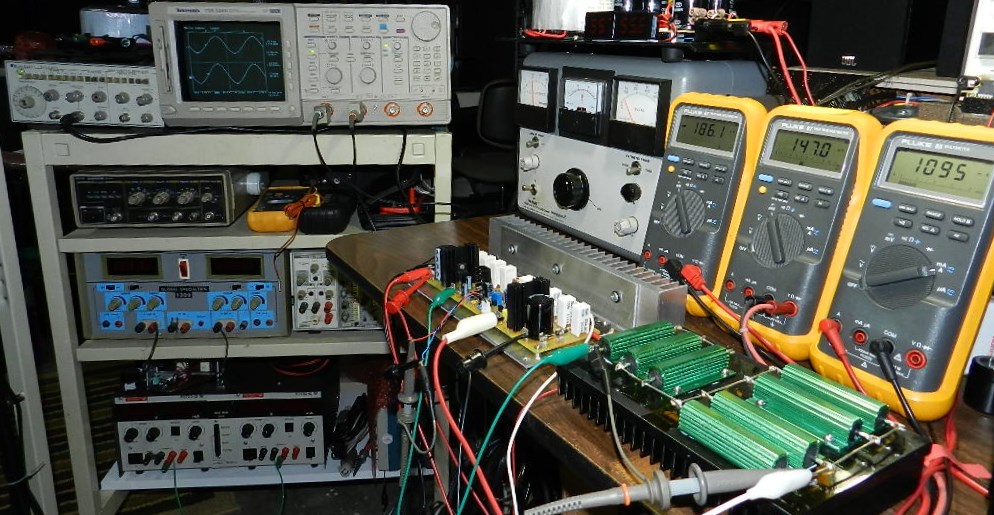
The next test procedure is optional, but if an oscilloscope, audio signal generator and 8Ω dummy load are available, the maximum power output before clipping occurs can be measured. Be careful not to touch the heat sink or the dummy load during this test, they will get very hot. After building Project 21, I’ve improved the dummy load’s heat sink and added more series-parallel connected power resistors for a total resistance of 8Ω and a combined power rating of 700watts, as shown in the picture on the left.
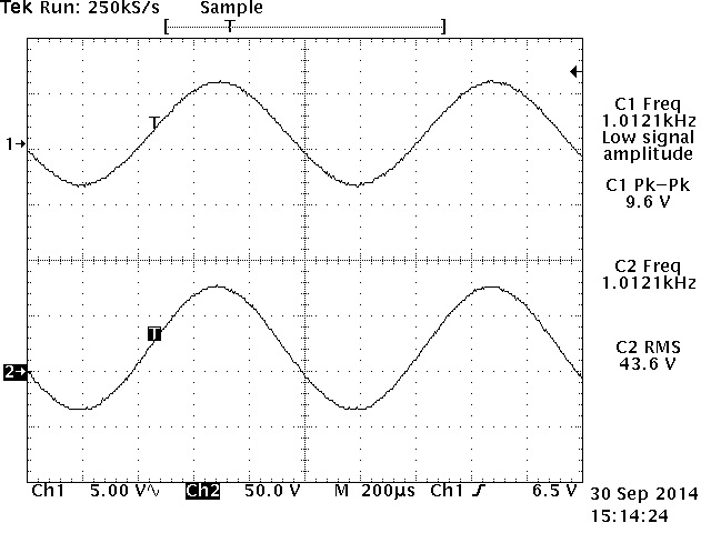
The power output was measured using an HP3312A Function Generator set at 1KHz 9.6Vp-p sine wave output and connected directly to the input of the amplifier under test as well as the CH1 test probe of the oscilloscope. An 8Ω/700Watt dummy load was connected at the output of the amplifier under test as well as the CH2 test probe of the Tektronix TDS520D 500MHz Digital Phosphor Oscilloscope. The amplifier under test produces 43.6Vrms across the 8Ω/700W dummy load or a power output of about 238Wrms, as shown in the TEK hardcopy picture on the right. The oscilloscope’s horizontal scale was adjusted at 200uS to verify for any visible clipping or artifacts on either peak. This project was paired with Project 9, the LM1036 tone control project.
What do I listen for music test? Download from Amazon: Guaji-Rita by Hector Martignon from Allegro 2011 Winter Sampler album, Bossa de Mank by Claudio Roditi from Allegro Fall 2011 Sampler album, Renewal by Monty Alexander and Bluesy Basie by Rossano Sportiello from Allegro Spring 2011 album and a techno album from Iboga Records Amazon Sampler (I’ve recently checked on 10-16-2014 and this is the only album that’s free since my last recommendation, play the Sao Paulo cut). Assuming you have a good sounding speaker and preamp, it should give you an idea, by comparison, of what I’m listening for music test or play your own favorite music!