
Project 2
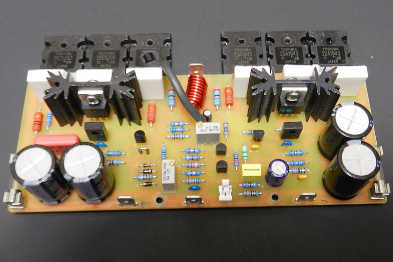
The circuit of Project 2 is similar to Project 1, except for the adjustment of the DC offset voltage which can be done manually. Another interesting change to the circuit is the very high value of the feedback resistor R17, twice that of Project1. The model unit uses 3 pairs of complementary 2SC5200/2SA1943 or 2SC5242/2SA1962 power output transistors.
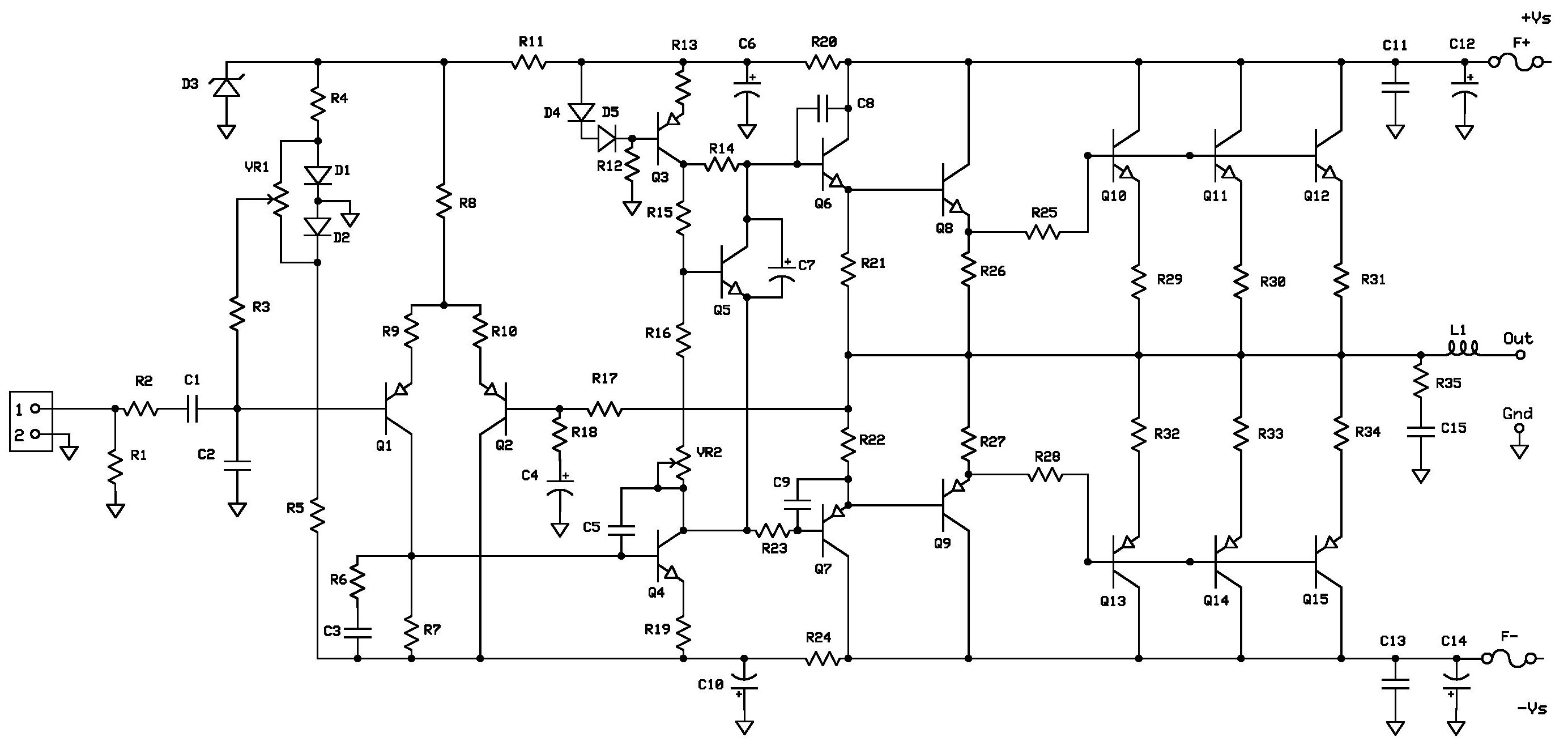 Schematic Diagram of Project2
Here's a brief description of the circuit:
The input stage is a differential amplifier circuit consisting of Q1/Q2. VR1, D1 and D2 connected at the base of Q1 controls the DC offset voltage. Notice the addition of R9 and R10 at the emitters of Q1 and Q2 were not present in Project1. R17 and R18 in series with C4 determines the overall gain of the amplifier. Q4 is the voltage amplifier stage, loaded by a current-source circuit Q3/D4/D5. The Miller cap, C5 compensates for high frequency. For D1, D2, D4 and D5 I use BAV21 with Vf of 1.25V at 200mA or you may use BAW27 with a Vf of about 1.12V at 400mA. VR2 controls the idle current of the power output transistors. Vbe multiplier, Q5, is populated off the PCB and attached to one of the power transistors for thermal feedback. The power output stage transistor drivers Q6, 7, 8 and 9 are configured as emitter followers, they isolate Q4 from the power output transistors.
The power output transistors Q10, 11, 12, 13, 14 and 15 are configured as full complementary push pull parallel output stage. I decided to add another pair of power transistors for this project so that higher power output can be achieved especially at lower impedance loads. No harm done if you prefer to use only 1 base resistor R25 and R27 respectively for each parallel-connected NPN and PNP power transistors, like I did. The emitter resistors R29 thru R34 connected at the output power transistors are necessary for thermal stability. L1, R35 and C15 improves stability of the amplifier at any loads. The main power supply rails are ±54VDC.
Now if you decide to build Project 2, then put together the printed circuit assembly (PCA), i.e. create and populate the PCB. A PCB layout and Bill Of Materials (Project2 BOM) are provided for free, as is, no warranty.
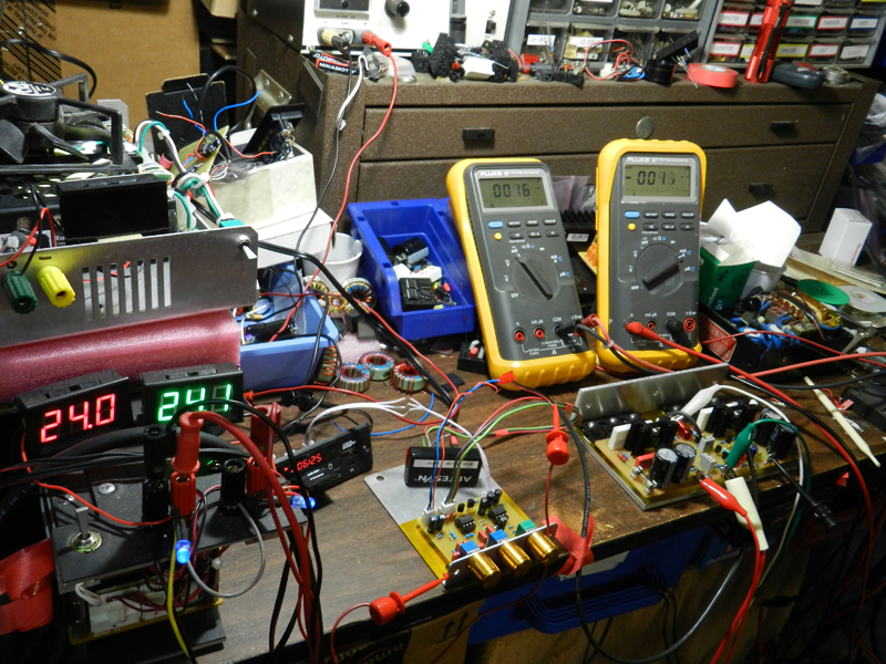
This is the fun part of the project once assembly is complete. Visually inspect the PCB for component orientation and polarity, trace shorts, cold solder and so forth. Flip the PCB to view the bottom copper side and using an ohmmeter* adjust VR2 to read almost 0Ω across its terminals. If you have a ±24VDC power supply use that for testing the amplifier. Connect 2 DMMs to monitor the ±24VDC power supply, 1 DMM to measure the DC offset voltage and 1 DMM to measure the idle current of the amplifier.
Why all the DMMs? The very first time you apply power to a newly built audio amplifier project the DMM is your best friend. The DMM tells you if there is something wrong with your circuit board assembly. A very high ammeter reading indicates that a component in the circuit is drawing too much current. The same goes with a very high voltage reading at the output of the amplifier where you should expect a very low voltage reading in the millivolts range. The DMM tells you the bad news and when that happens you immediately switch OFF the power supply and recheck the assembly. If you don't have a DMM when that happens, you have only your senses to tell you something is burning and that smoke signals are coming from the PCB.
With the power source switched to OFF, remove the F+ fuse and insert a milliammeter* at the fuse terminals. Connect a millivoltmeter* at the output pcb terminal to ground. Switch power supply to ON. If you did a good job, the millivoltmeter* connected at amplifier’s output will read some DC voltage value. Adjust VR1 to get as close to 0.0V, the model unit was adjusted at 1mV, this is the DC offset voltage. The voltmeters* connected at the power supply should read whatever voltage you apply to the amplifier under test and should not change. Initially adjust VR2 to read 20 mA on the milliammeter* connected at the F+ fuse terminals. After a warm-up period of 30 minutes readjust to 40mA, this is the idle current of the amplifier. After you've made all the adjustments, proceed to music test.
Connect a test speaker and plug in your favorite signal source. The good thing about this project is that it works at ±24VDC with amazing results. I paired this project with the LME49720-inspired tone control circuit and featured as PreAmp 1 in the PreAmp section of this website.
Other than mentioned, power OFF immediately and recheck assembly.

Project 2 installed on a thick 0.180” aluminum-mounting bracket, which can be attached to an extruded heatsink.
Project 2 is shown under initial test. VR1 is adjusted to about 1.6mV and VR2 is adjusted at about 10 to 20mA.

Project2 Bottom Copper Layer

Project2 Silkscreen Parts Placement Layer
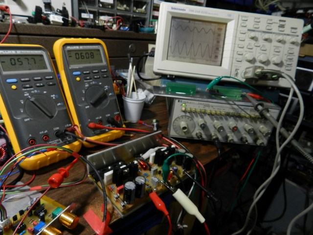
Project2 Under another test. A 1Vpp 1KHz sine wave input signal resulted to about 30Vpp across an 8Ω 100Watt load . The projects’ aluminum bracket warms up during this test, but stays normal cool during music test.
*this refers to one of the basic functions of a DMM.