Project 27
The idea for modeling Project 27 was inspired by the book “Designing Audio Power Amplifiers” written by Bob Cordell. Is it worthwhile to actually build a prototype of the 200-watt rated version of the amplifier mentioned in the Power Amplifier Design Evolution chapter? After a quick email to Bob, I’ve then decided to build the circuit design from his book and presented on this website as Project 27. But before going any further, on behalf of BuildAudioAmps’ registered members, I would like to express our sincere thanks to Bob and other authors like him, for giving us better understanding and insights relating to audio power amplifier design.
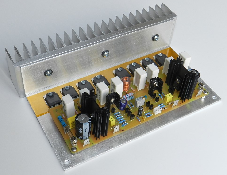
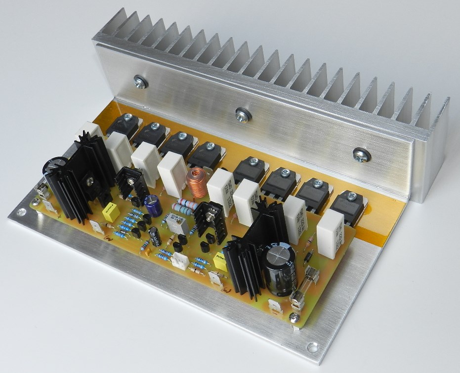
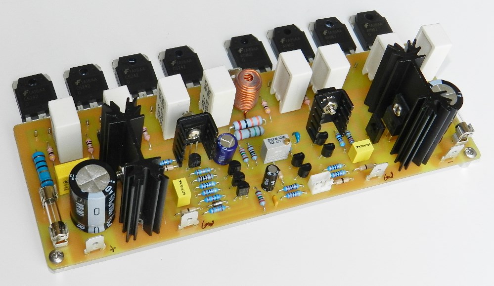
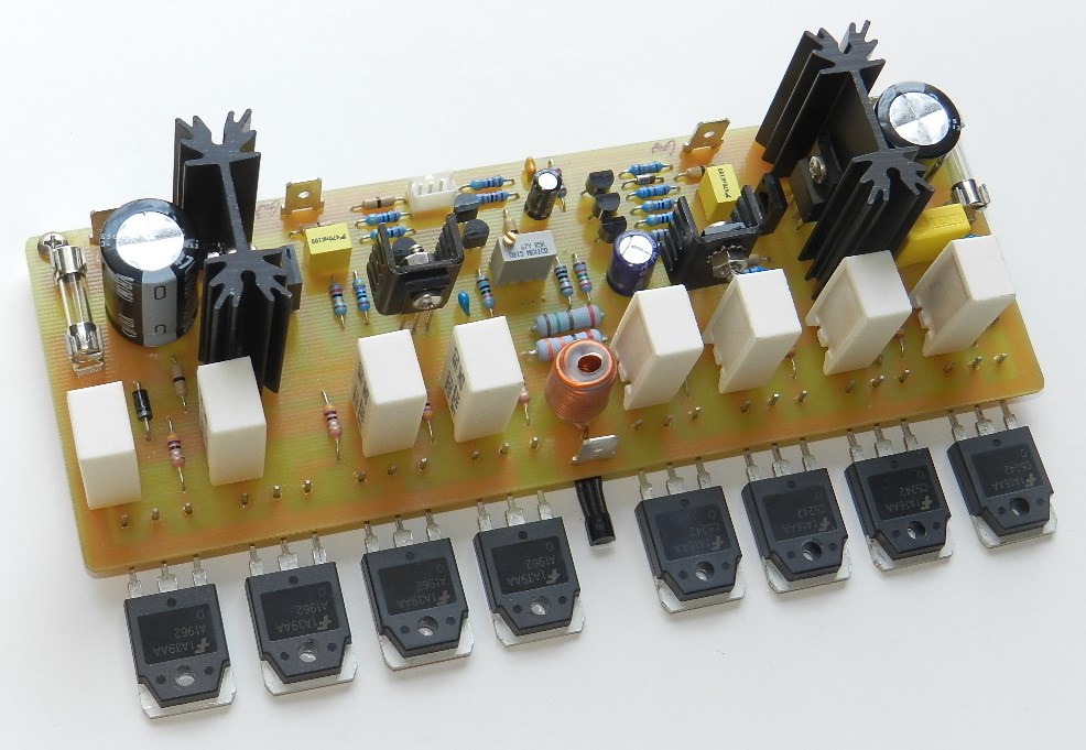
The theory of operation of the evolving high-powered amplifier design was well explained in the book and there’s no need to mention it again on this website. However, I have to point out that several passive components were added at the input, output and the feedback path of the simplified schematic diagram (well described in the last part of the chapter) to make Project 27 a complete working audio power amplifier. Furthermore, minor modifications were made to the suggested design as shown in the schematic diagram. The Vbe multiplier circuit was also modified so that the bias of the power output devices can be made adjustable. You have two options for this project depending on the power supply that you may already have somewhere. The first option is powered by ±35VDC that produces a power output of 60Wrms into 8Ω and the second option is powered by ±64VDC that produces a power output of 225Wrms into an 8Ω load.
If you’re interested in building this project and have read the Information and Policies section of this website, the schematic diagram, PCB layout (available only by request) and BOM are free, as is, no warranty.
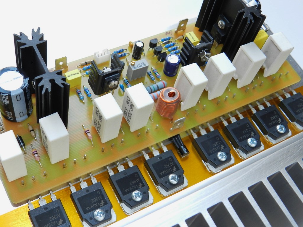
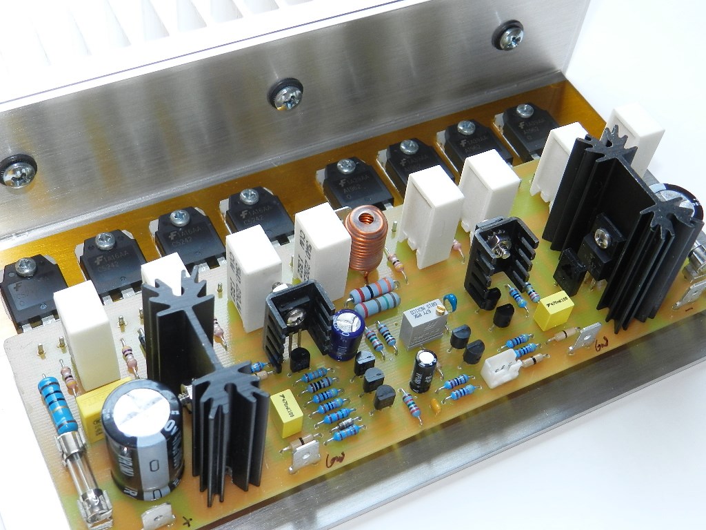
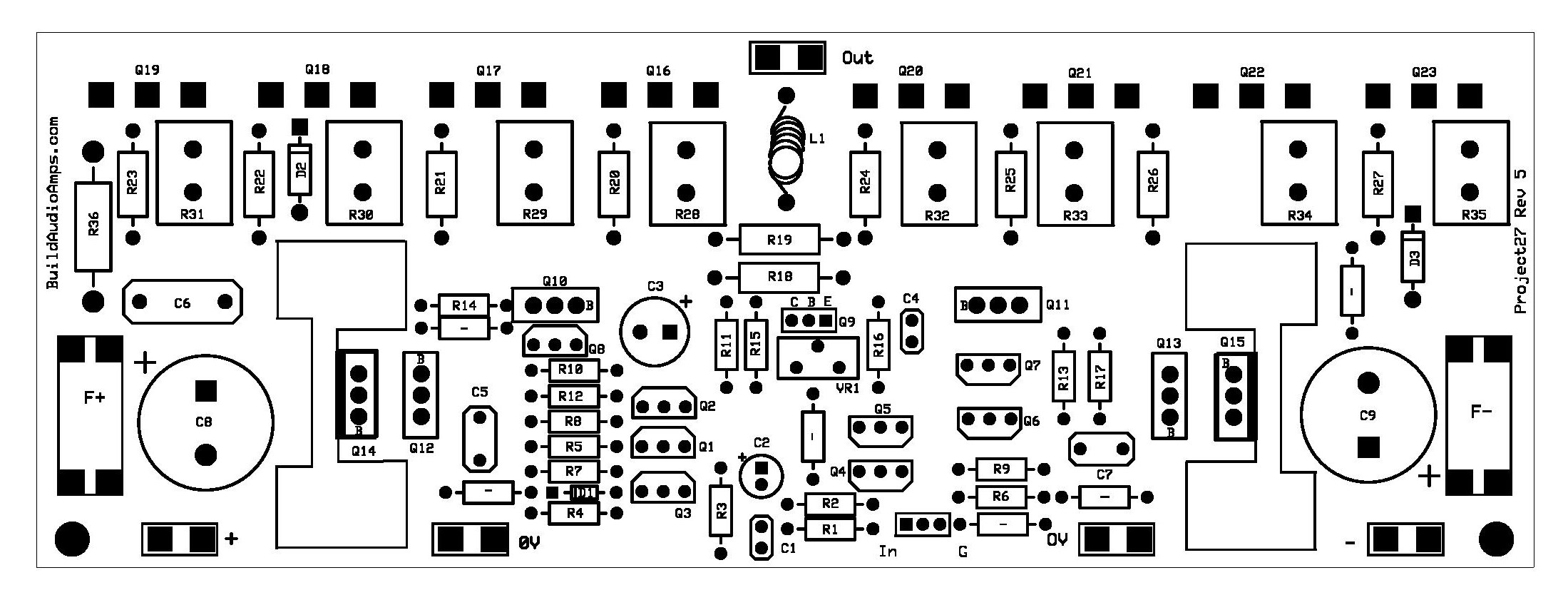 Silkscreen Parts Placement Layer of PCB for Project 27.
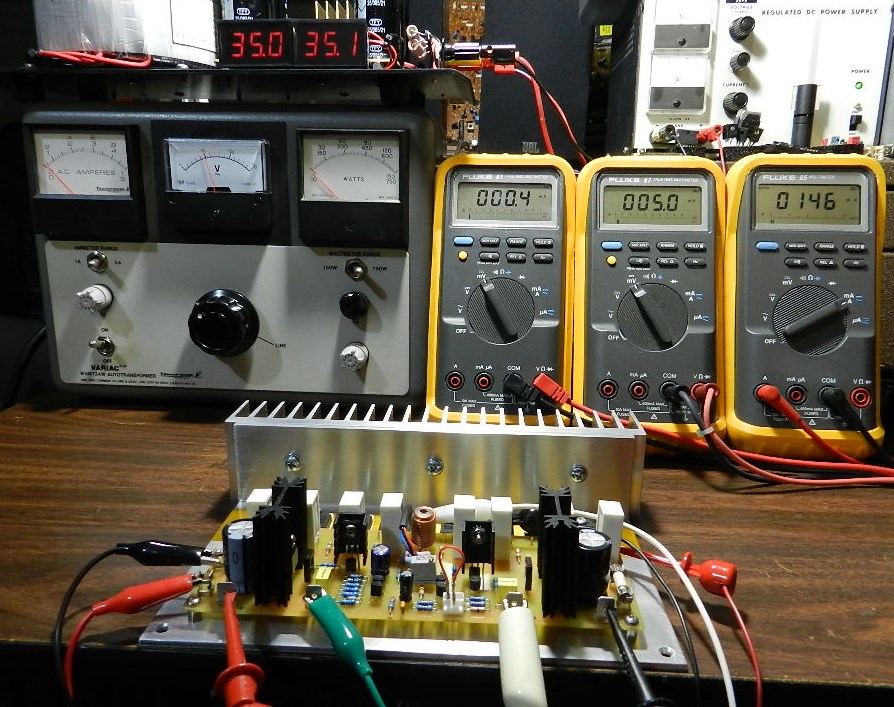
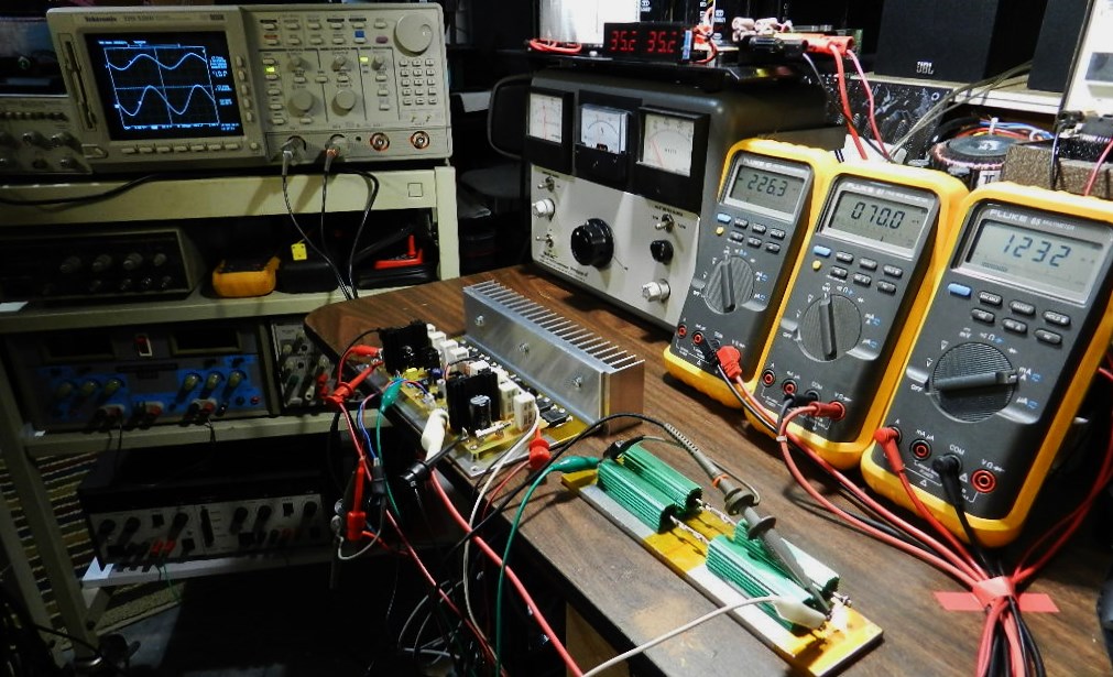
The low-voltage option of Project 27 will utilize a ±35VDC power supply. Short the input of the amplifier to ground by connecting a jumper wire or shunt at J1 and do not connect any load or loudspeaker at the output. If your PCB’s project will be mounted similar to those shown in the pictures, be sure to measure the insulation resistance between the collectors of all power output transistors and the metal mounting bracket or heatsink. Q9 was wired and mounted off the PCB to the metal mounting bracket by a small piece of double-sided thermal tape (Sekisui #5760) similar to the ones used for attaching a heatsink to a CPU, GPU or RAM in PCs.
The following DMM readings are for normal conditions, assuming that you’ve built the project’s PCB without assembly errors. The DMM on the left side of the picture is measuring the DC offset voltage of the amplifier at 0.4mV. The DMM in the middle is measuring the voltage drop across the emitter resistor of Q19 at about 5mV after a warm-up period of 10 minutes; adjust VR1 to obtain this value. The DMM on the right side of the picture is measuring the current across the F+ fuse terminals at approximately 146mA. If you chose this option to power the project with ±35VDC and had obtained same test results you may continue with music test, listen and enjoy!
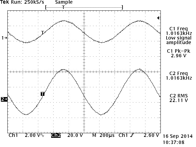
The next test is optional, but if an oscilloscope, signal generator and an 8Ω dummy load are available, you can check the maximum power output of the project before clipping occurs. Be careful not touch the heatsink or the dummy load during this test; they will get hot! An HP3312A function generator was set for a sine wave 1KHz 2.96Vp-p output and connected directly to the input of the amplifier as well as the CH1 probe of the Tektronix TDS520D oscilloscope. The CH2 probe of the oscilloscope and the 8Ω dummy load was connected at the output of the amplifier under test and measured 22.11Vrms or a power output of approximately 60Wrms with no visible clipping, as shown in the Tek hardcopy picture below.
The high-voltage option of Project 27 uses a ±64VDC power supply rails. The power supply was built with a toroidal power transformer rated at 300VA 90VCT, KBU3510 bridge rectifier and 10,000uFd/80V filter capacitors. If better regulation is desired without objection to cost, then add more reservoir filter capacitors.
If a Variac transformer is unavailable, make sure that the power supply has been properly built and that the output voltage rails have been measured at approximately ±64VDC. With the power supply switched to OFF, connect a jumper or shunt at the input of the amplifier and do not connect any load or loudspeaker at the output. Adjust VR1 for minimum resistance. VR1’s resistance can be measured at the south end of R15 and R16, please refer to the schematic diagram and silkscreen layer of PCB. Switch the power supply to ON; the DMM measuring the voltage drop across the emitter resistor of Q19 should read less than 1mV. If the DMM reading is more than 1mV and cannot be adjusted, power OFF immediately and check the PCB for assembly errors. If the DMM reading is less than 1mV, wait for 10 minutes for the bias to stabilize and then slowly adjust the reading to 5mV.
If a Variac transformer is available, connect the AC input of the power supply to the output of the Variac transformer. The Variac transformer shown in the picture has AC ammeter, voltmeter and power meter, which are very useful for this type of test setup. Switch the power to ON and carefully adjust the Variac’s AC output voltage from zero until the power supply reaches the required ±64VDC rails. Keep an eye on unexpected increase in any of the DMM or the Variac’s meter readings, if you did, power OFF immediately and check the PCB for assembly errors, if not, you may proceed with the test.
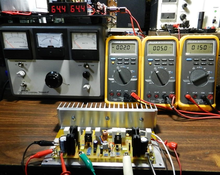
The following DMM readings are for normal conditions and is assuming that you did a good job on the PCB assembly. The DMM on the left side of the picture is measuring the DC offset voltage of the amplifier at 2mV. The DMM in the middle is measuring the voltage drop across the emitter resistor of Q19 at 5mV after a warm-up period of 10 minutes; adjust VR1 to obtain this value. The DMM on the right side of the picture is measuring the current across the F+ fuse terminals at 150mA. If you chose this option and had obtained same test results you may proceed with music test. Out of the tinkerer’s curiosity, the Variac was adjusted so that the output of the power supply goes down from +/-64VDC to +/-5VDC, then run a music test. The music quality it reproduced was surprisingly very good at such a very low voltage level!
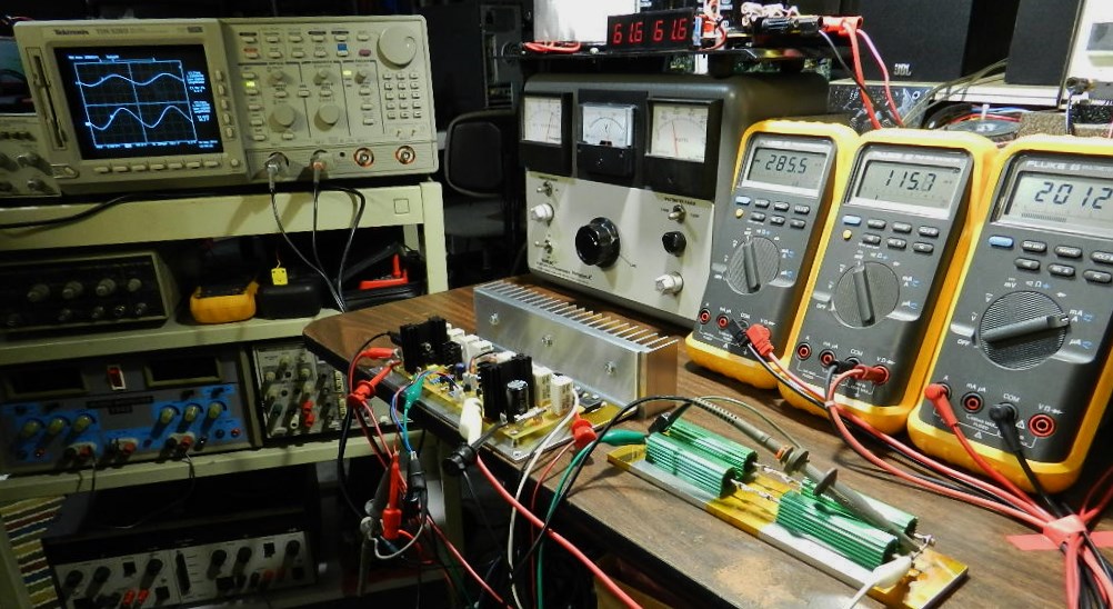
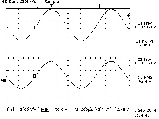
The next power output measurement test is optional and uses the same ±64VDC power supply rails. Be careful not to touch the heatsink or the dummy load during this test; they will get extremely hot! An HP3312A function generator was set at 1KHz sine wave output signal with the amplitude at this time adjusted to 5.36Vp-p and connected directly to the input of the amplifier. The Tektronix TDS520D oscilloscope measured 42.4Vrms across the 8Ω/400W dummy load or a power output of about 225Wrms with no visible clipping on either peaks, as shown in the Tek hardcopy picture above. The power amplifier is capable of producing more power output when driving a 4Ω load. Overall, in my opinion, Project 27 was worth building and reproduces music fidelity that will not disappoint!
Updated 10/27/2014:
The prototype model’s idle current was adjusted conservatively at 5mV across the emitter resistors. If you plan to build this project, you might consider Bob’s suggestion to adjust the idle to 26mV according to his design criteria:
“I think 5mV across each emitter resistor is too low. However, I understand your concern about heat at idle. The total bias current at idle will depend on your choice of the value for RE. For example, if RE = 0.33 ohms, then total current in the design will be 4 * 26mV/0.33, or 4 * 79mA = 315mA. If you have +/- 50V rails, idle dissipation will be 31.5 watts.” -Bob