Project 32
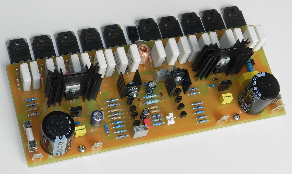
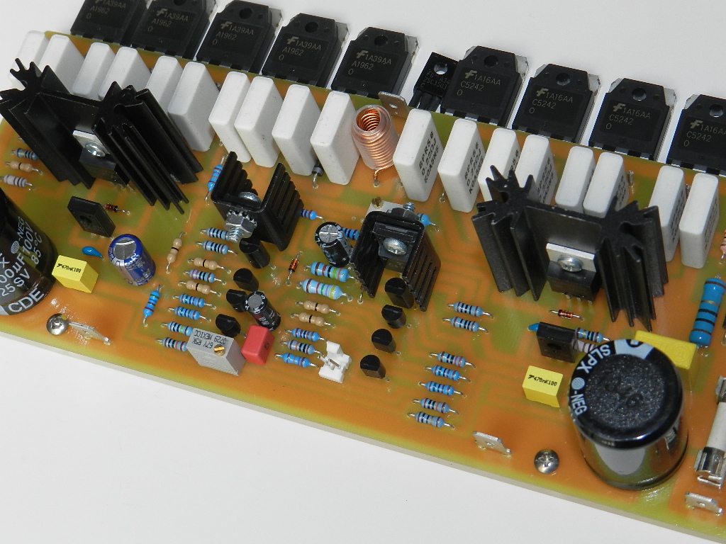
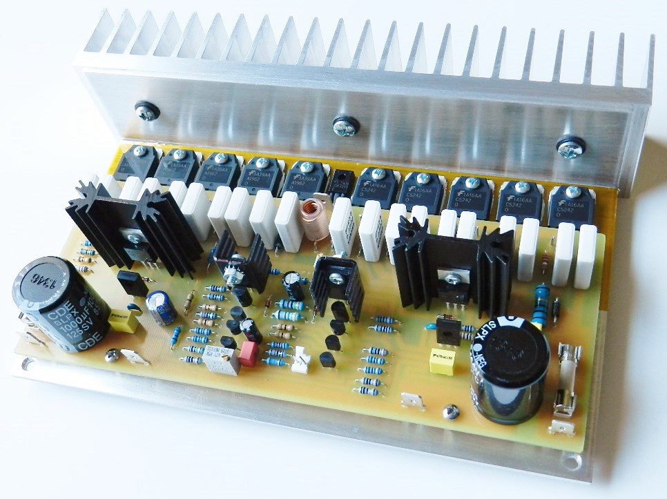
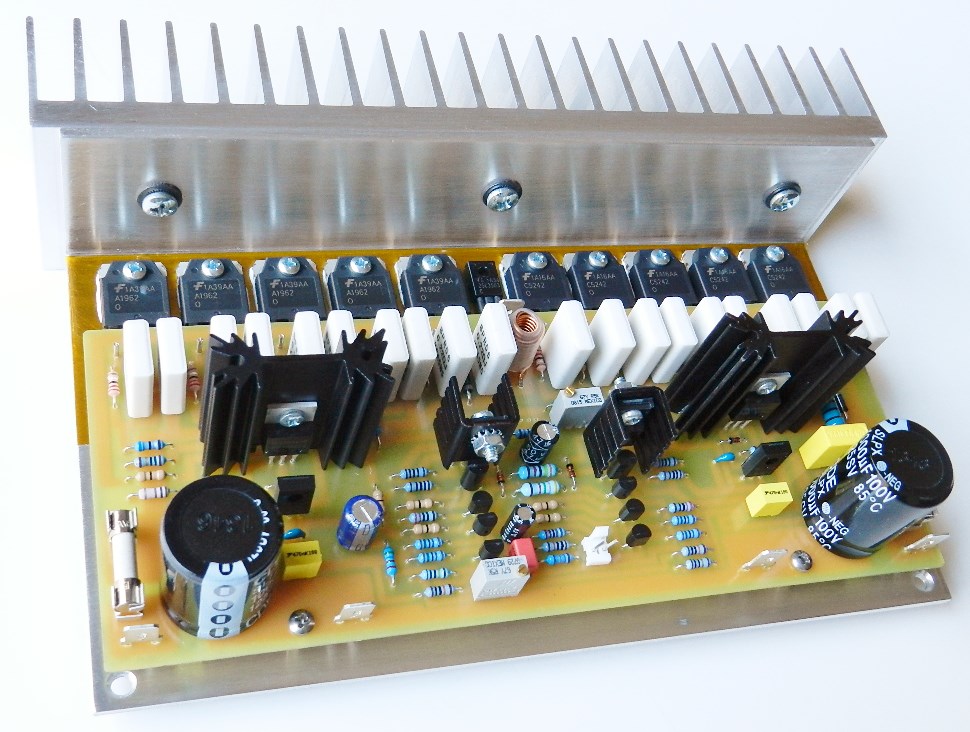
The circuit of Project 32 is a full complementary-symmetrical input stage topology similar to the previous project and a CFP (Complementary Feedback Pair), also known as the Sziklai pair power output stage. This project takes advantage of the superior audio quality of the input stage combined with the wider bandwidth performance of a CFP-based power output stage. The combination, in my opinion, resulted in a surprisingly excellent audio quality. The amplifier’s overall output is taken from the collectors of all power output transistors by way of R46 through R55. If that’s not enough R41 ~ R48 and R49 ~ R60 were added at the emitters of all power output transistors for stability. There’s a total of 20 pieces of KOA Speer resistors, which have a smaller PCB component footprint to save PCB space, as shown in the heading pictures. The measured power output of this project is about 206Wrms for an 8Ω load or more for a 4Ω load with a power supply of ±64VDC rails.
If you plan to create your own PCB layout, make sure that the ground trace of input J1 must be laid out farther away from the main power ground. A 10Ω resistor was added to lift the ground that reduces noise to a negligible level. A voltage divider along with VR1 was added at the input stage to conveniently trim the DC offset voltage to minimum.
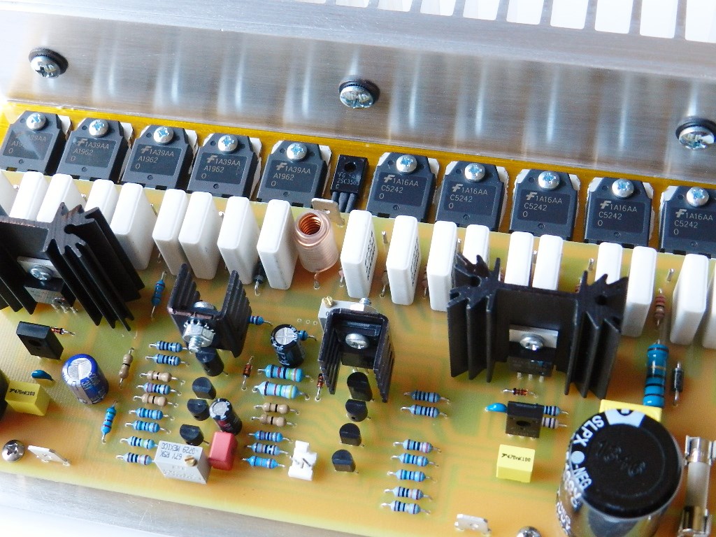
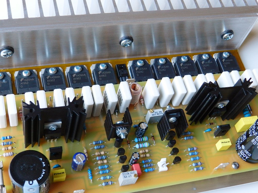
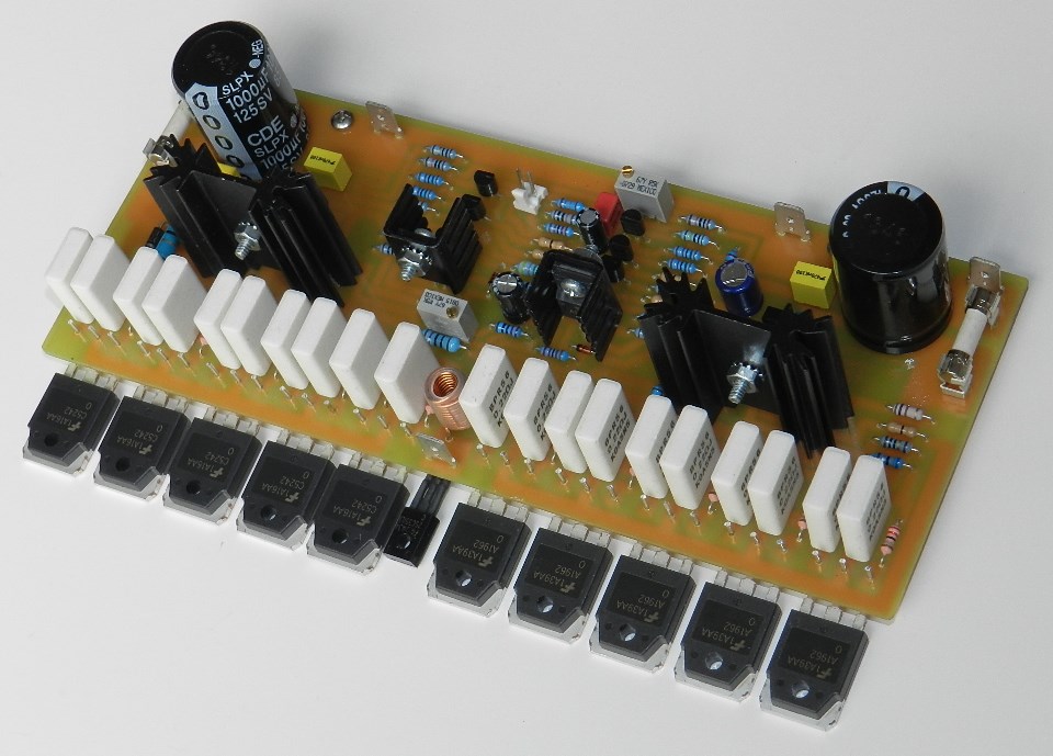
Keen-eyed readers will notice the heading pictures of the prototype model shown above are at Rev1 while the PCB silkscreen parts placement layer is at Rev2, shown below. Changes were made to the voltage amplifier stages to match with the harsh requirements of a stable CFP-based power output stage. If you are interested in building this project and have read the Information and Policies section of this website, the schematic diagram, PCB layout (available by request) and BOM are free, as is, no warranty.
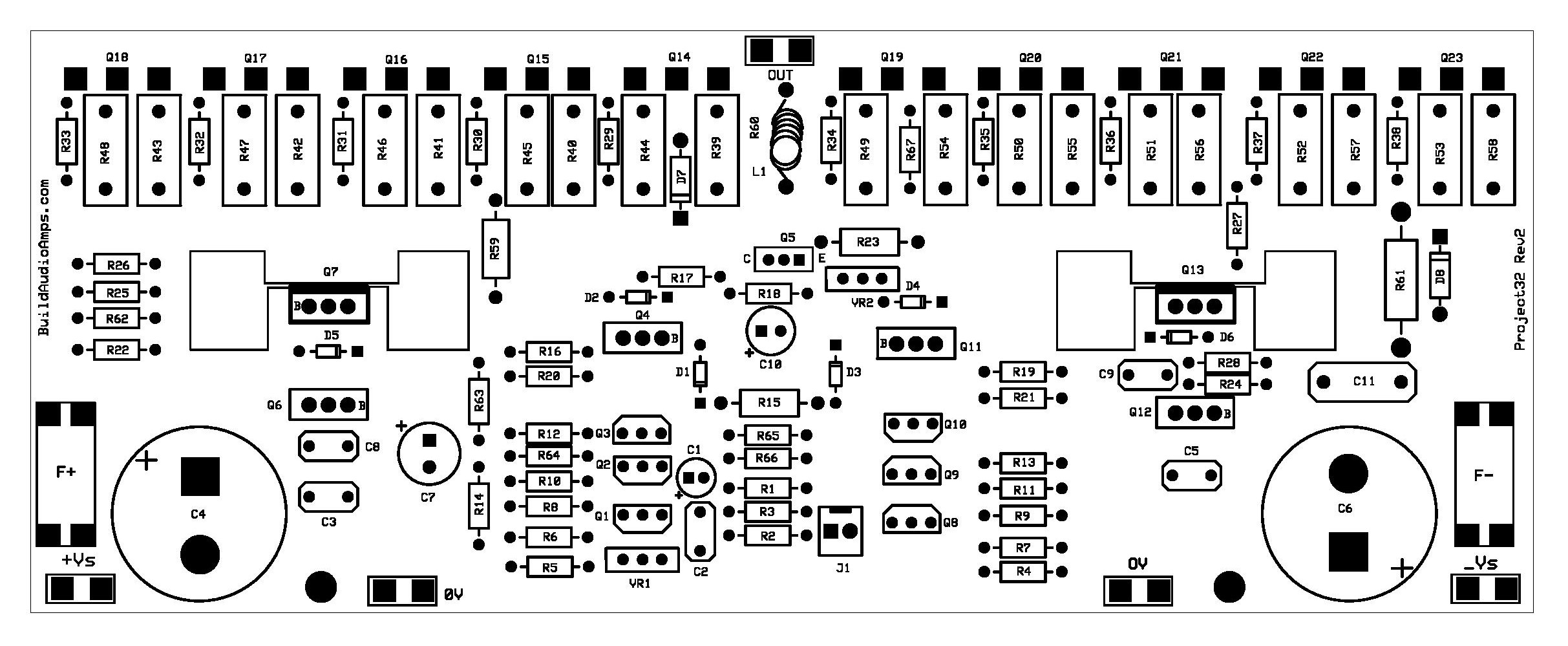 Project 32 Silkscreen Parts Placement Layer of PCB.
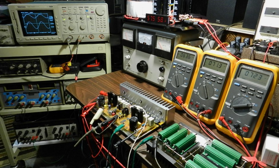
If you’ve decided to build this project, the DC offset voltage and the idle current needs to be adjusted first before going any further. Insert a jumper or shunt at the input of the amplifier. Do not connect any load or loudspeaker at the output of the amplifier. Adjust VR2 to a maximum resistance of 5KΩ; please refer to the schematic diagram where to access VR2 on top of PCB. Prepare 3 DMMs to measure the DC offset voltage at the output of the amplifier, the voltage between all the collectors of the PNP and NPN power output transistors and the current across the F+ fuse terminals. Experienced amp builders have more than 3 DMMs.

If a Variac transformer is available, connect the AC input of the project’s power supply to the output of the Variac transformer. Switch the power to ON and gradually adjust the Variac’s AC output from zero until the voltage output of the power supply reaches ±64VDC while keeping an eye on sudden increase in any DMM readings. If you have observed a sudden increase in any of the DMM readings, switch the power to OFF immediately before any populated component vaporizes and check the PCB for assembly errors. The picture above shows a DC offset voltage at 0.4mV; adjust VR1 to get to this value or less. The voltage across all the collectors of PNP and NPN power output transistors was measured at 10.9mV; adjust VR2 to read from 5mV to 10mV. Readjust VR2 to get the 5mV to 10mV reading after a warm-up period of approximately 10 minutes. The current across the F+ fuse terminals was measured at 141mA, this value is dependent on the adjustment of VR2. If you obtain similar DMM readings, you may proceed with music test!
If a Variac transformer is unavailable, make sure that the power supply has been properly built and that the output voltage rails have been measured approximately ±64VDC before connecting it to the project. With the power supply at OFF, adjust VR2 for maximum resistance. Switch the power supply to ON; the DMM measuring the voltage across all the collectors of PNP and NPN power output transistors should read less than 1mV. If the DMM reading is more than 1mV and cannot be adjusted by VR2, power OFF immediately and check the PCB for assembly errors. If the DMM reading is less than 1mV wait for about 10 minutes until the bias have stabilized and then carefully adjust the reading from 5mV to 10mV. Adjust VR1 to set the DC offset voltage for minimum or within ±10mV DMM reading at the output of the amplifier, after that, you may proceed with music test!
The next test procedure is optional, but if an oscilloscope, audio signal generator and 8Ω dummy load are available, the maximum power output before clipping can be measured. Be careful not to touch the heatsink or the dummy load during this test, they will get very hot!

The power output was measured using an HP3312A Function Generator set at 1KHz 1.92Vp-p (just before clipping occurs) sine wave output and connected directly to the input of the amplifier under test as well as the CH1 test probe of the oscilloscope. An 8Ω/700Watt dummy load was connected at the output of the amplifier under test as well as the CH2 test probe of the Tektronix TDS520D 500MHz DPO. The project’s prototype model produced 40.6Vrms across the 8Ω/700W dummy load or a power output of about 206W or more than 400W for a 4Ω load, as shown in the TEK hardcopy picture on the right. The oscilloscope’s horizontal scale was adjusted at 200uS to verify for any visible clipping or artifacts on either peak. This project was auditioned with Project 9, the LM1036 tone control project, with very impressive results!