
TDA8950J
The TDA8950 is a high-efficiency Class D 2-channel audio power amplifier chip. The typical power output is 150Watts per channel with a speaker load impedance of 4 Ω. The TDA8950 chip operates over a wide supply voltage range from ±12.5 V to ±40 V and features low quiescent current consumption.
Features of TDA8950:
- Symmetrical operating supply voltage range from ±12.5 V to ±40 V
- Stereo full differential inputs, can be used as stereo Single-Ended (SE) or mono Bridge-Tied Load (BTL) amplifier
- High output power in typical applications:
SE 2 × 150 W, R L = 4 Ω (V P = ±37 V)
SE 2 × 170 W, R L = 4 Ω (V P = ±39 V)
SE 2 × 100 W, R L = 6 Ω (V P = ±37 V)
BTL 1 × 300 W, R L = 8 Ω (V P = ±37 V) - Low noise
- Smooth pop noise-free start-up and switch off
- Zero dead time switching
- High efficiency
- Low quiescent current
- Advanced protection strategy: voltage protection and output current limiting
- Thermal FoldBack (TFB)Fixed gain of 30 dB in SE and 36 dB in BTL applications
- Fully short-circuit proof across load
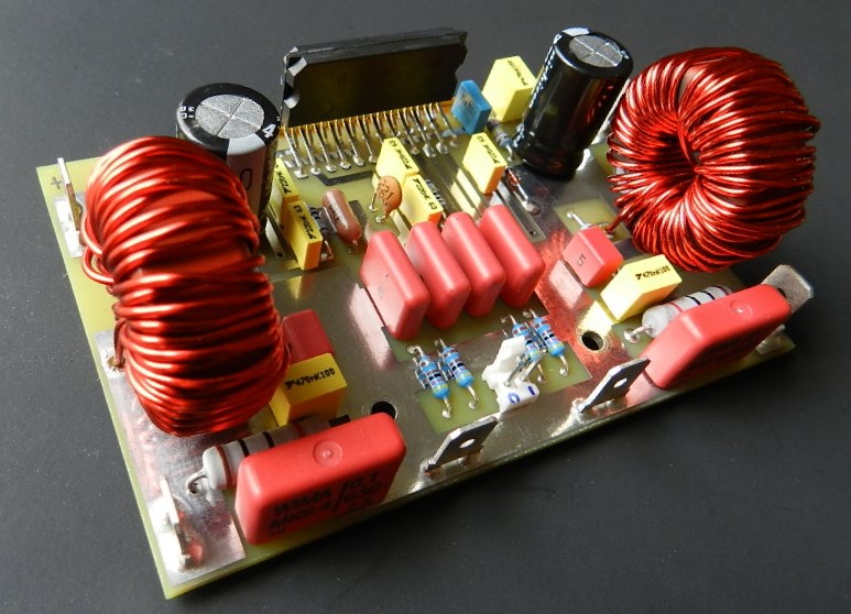
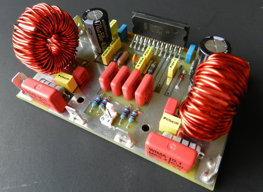
For this project the TDA8950 is configured as a mono Full Bridge Class D power amplifier. This configuration was chosen to effectively avoid a strange phenomenon of a typical Class D power amplifiers called "pumping effect".
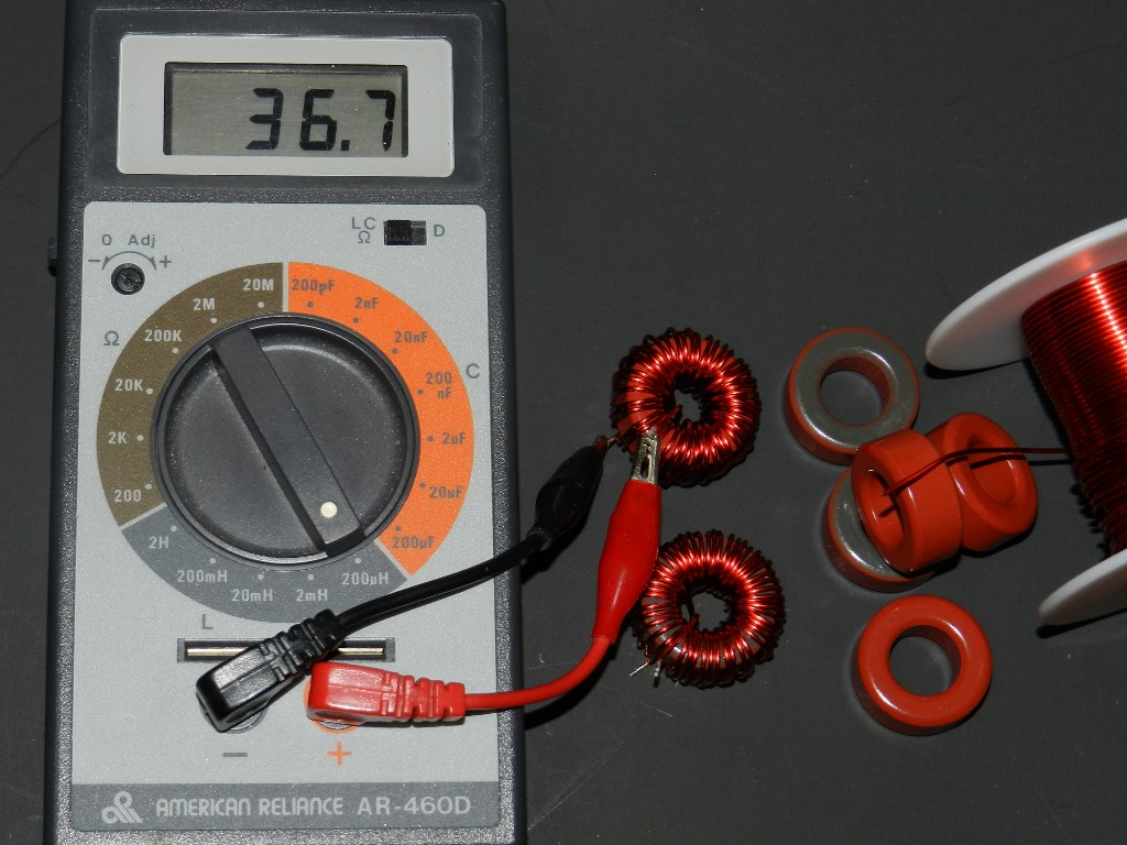
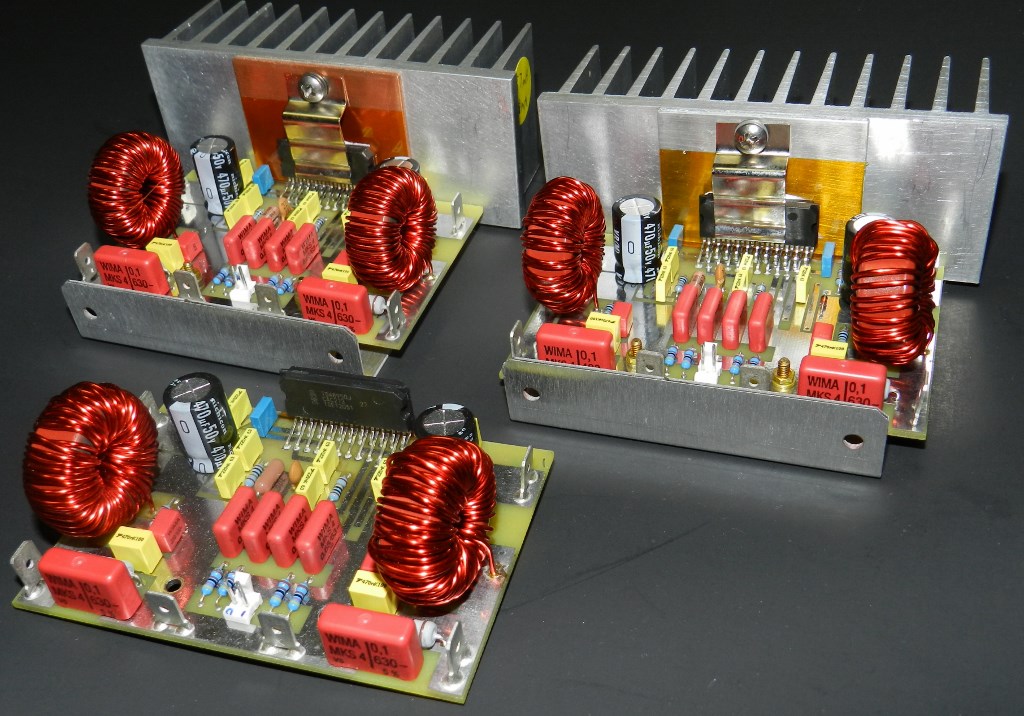
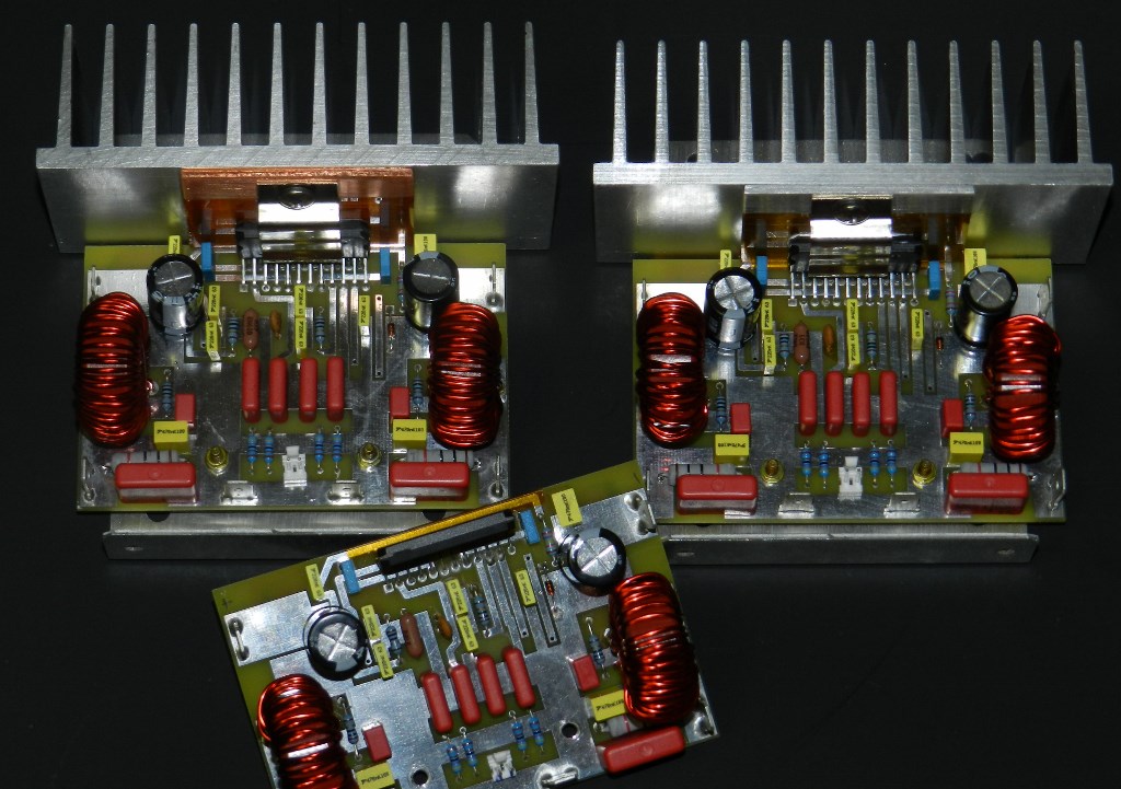
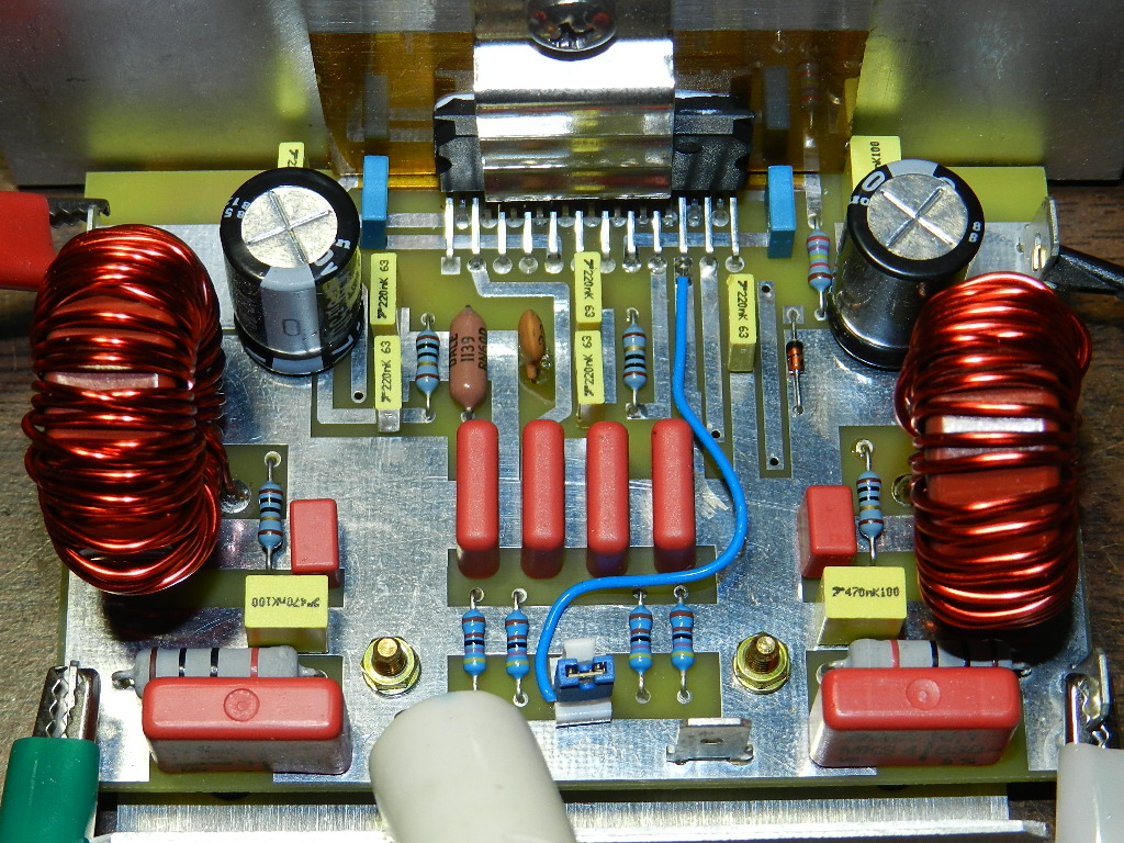
The tricky part of building this project is the toroidal-cored low pass filter inductors, L1 and L2. The inductor is made up of 75” of 18AWG enameled copper wire wound on a T106-2 core. After winding the coil, verify the inductance with an LCR meter, it should read about 37uH. With this value the idle current of the amplifier is about 48 to 50mA. The original NXP Semiconductors' schematic diagram of this project as well as other information about TDA8950 are found here: TDA8950 datasheet. However, if you're interested in building this project and have read the Information and Policies section of this website, the schematic diagram, PCB layout (available only by request) and BOM are free, as is, no warranty. Enjoy!
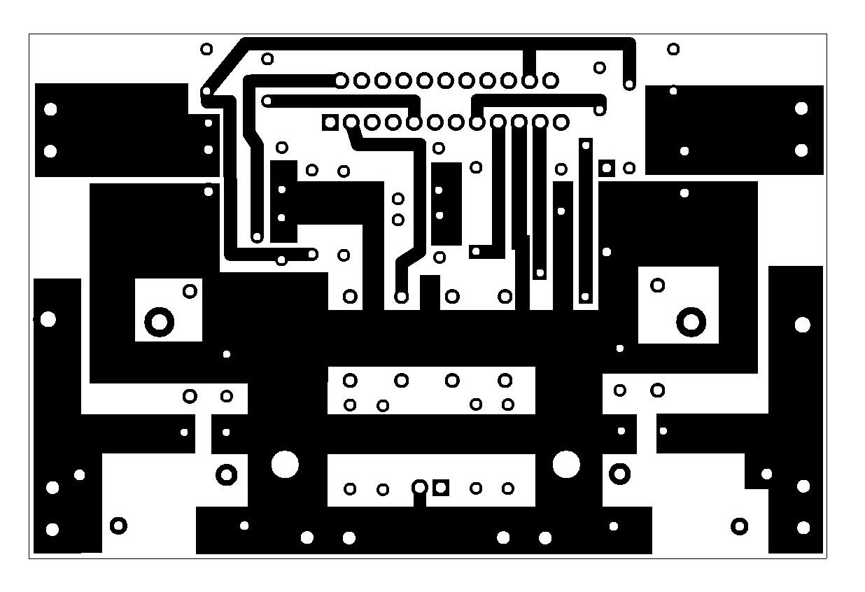
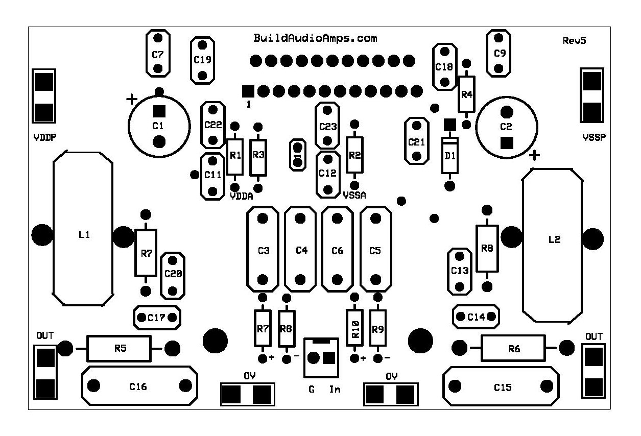
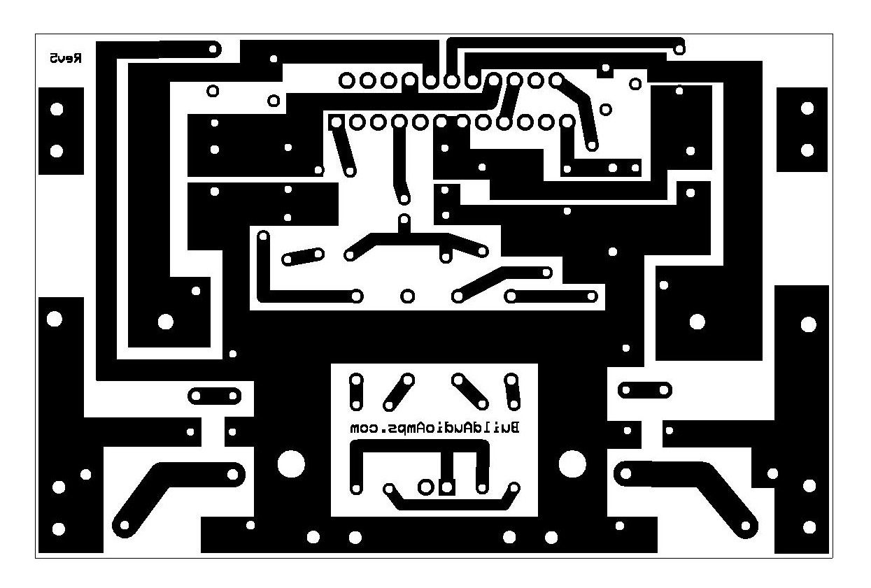
TDA8950J Top Layer TDA8950J Silkscreen Parts Placement Layer TDA8950J Bottom Copper Layer
Updated 12-22-2014
Cut the copper trace that runs from pin2 of J1 to the main ground (see top layer of PCB). Solder a piece of hook-up wire from pin2 of J1 to pin19 of TDA8950 (see picture below). This will eliminate the high-pitched noise caused by signal/power grounding problem and improves overall sound quality. When testing the project without a pre-amp it is necessary to install a shunt or jumper at J1, also shown in picture below. The update is not needed when the project is powered at ±25VDC rails.
![]()