Project 60
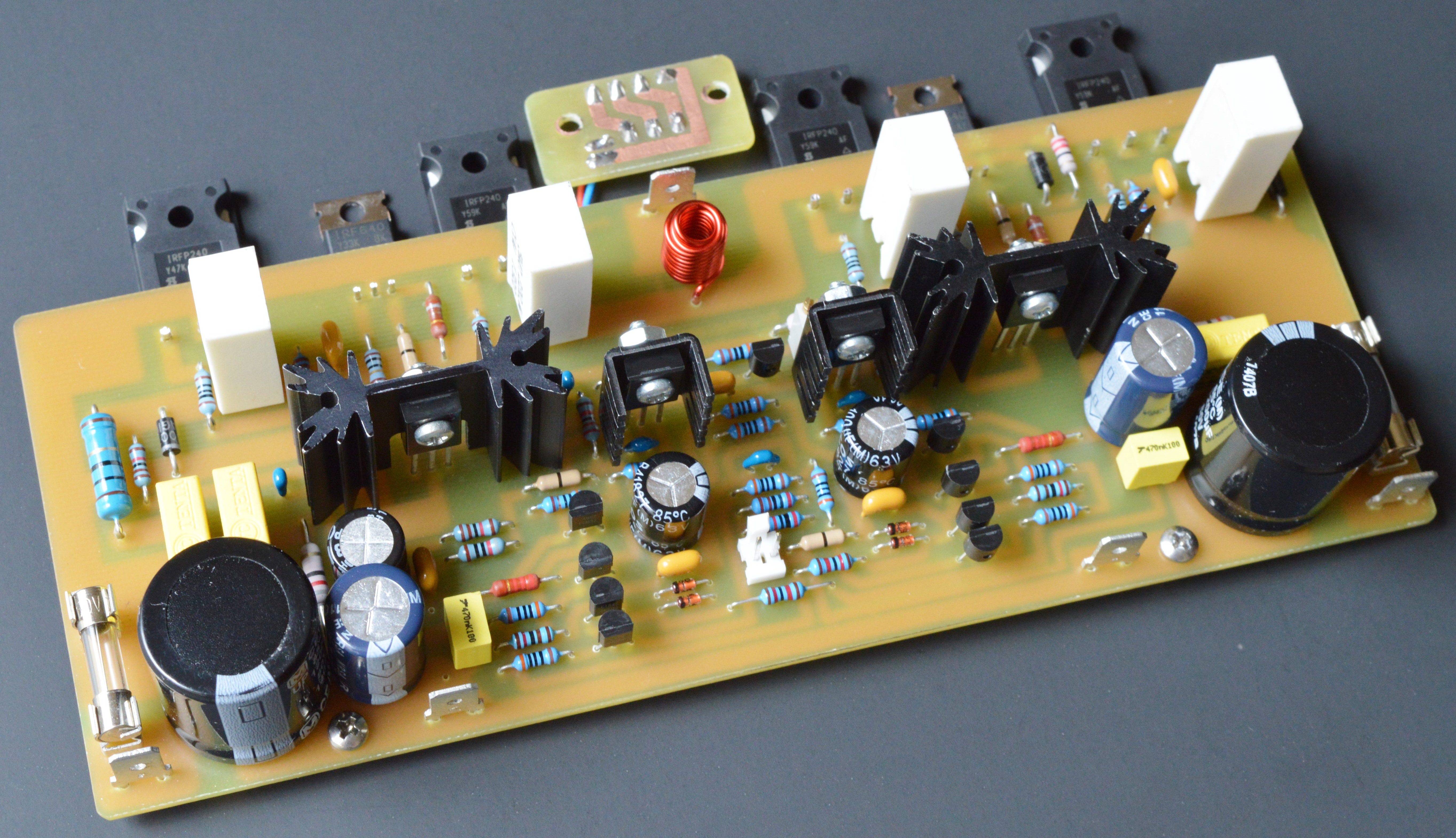
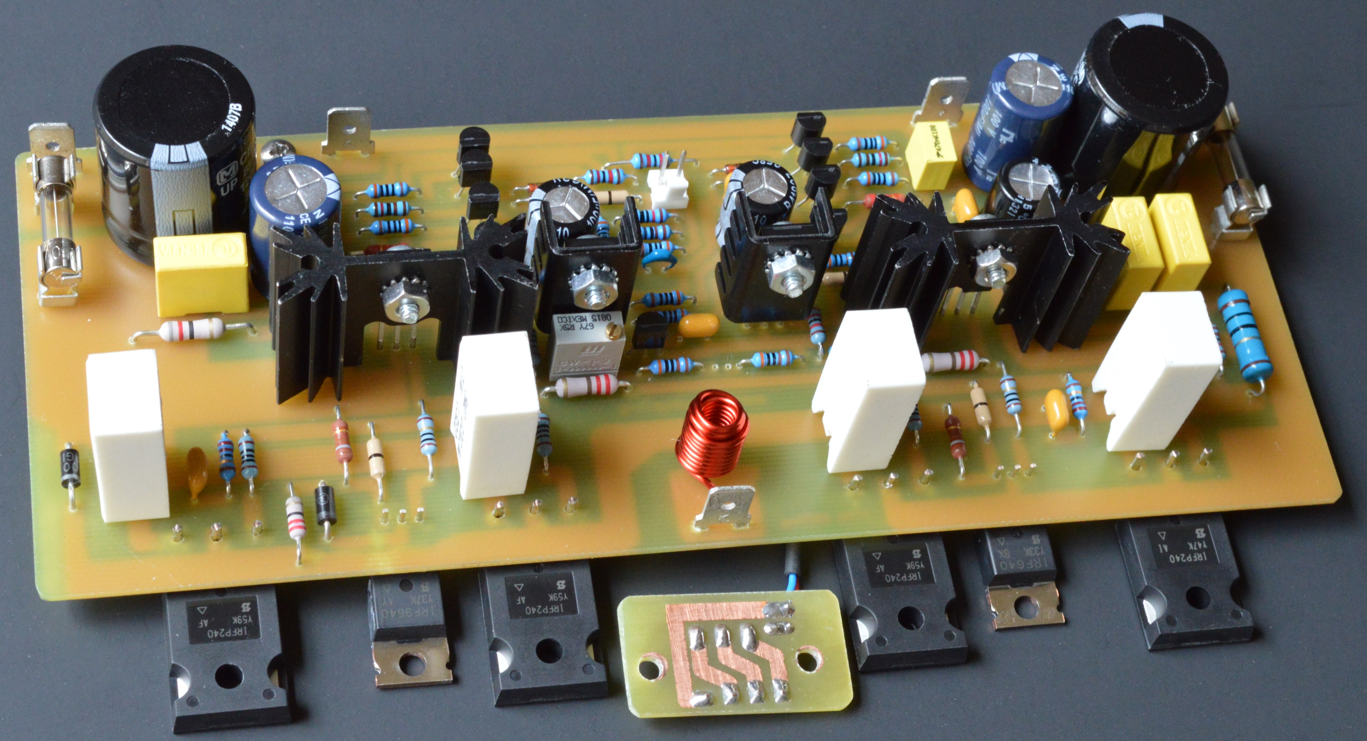
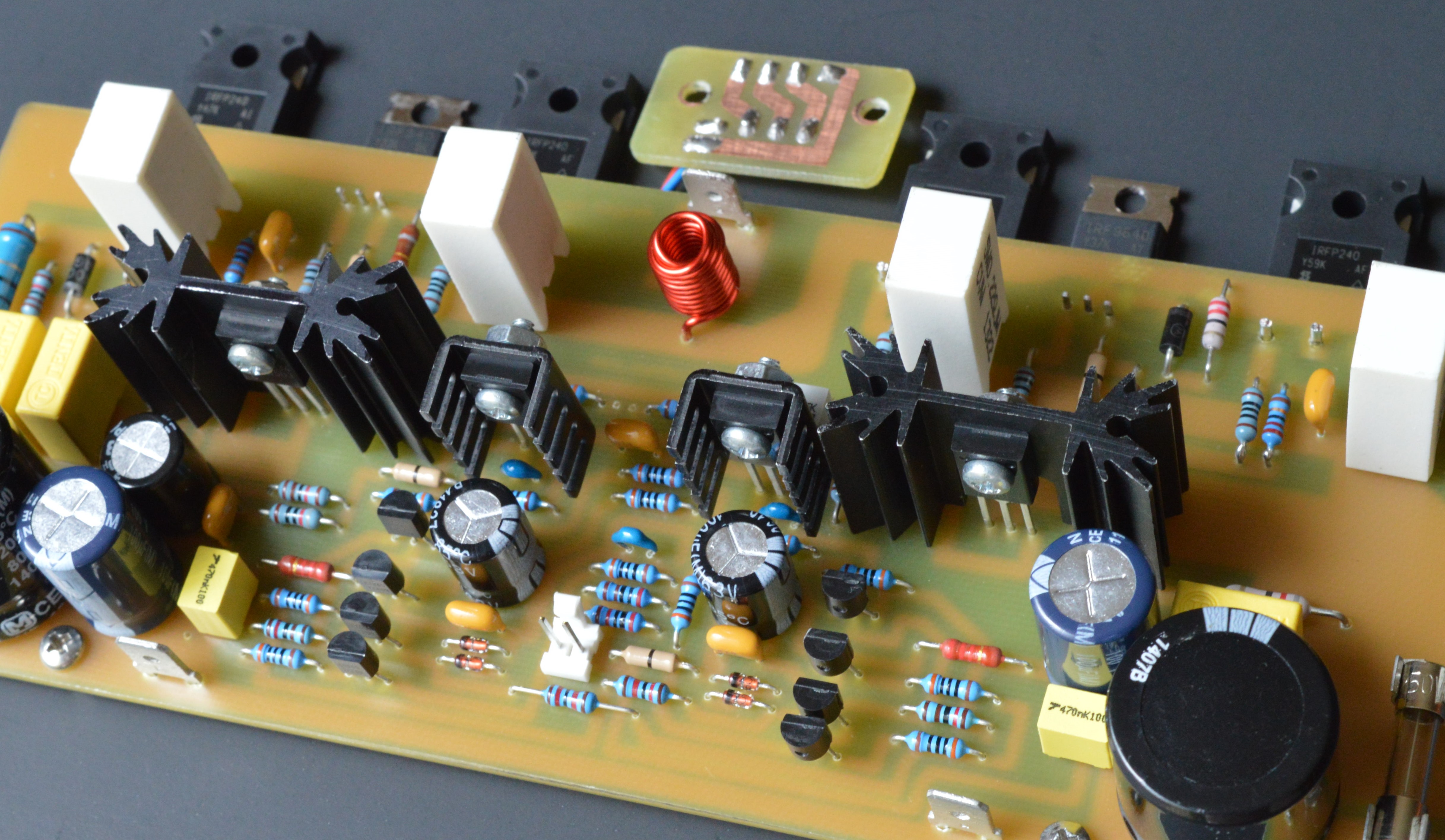

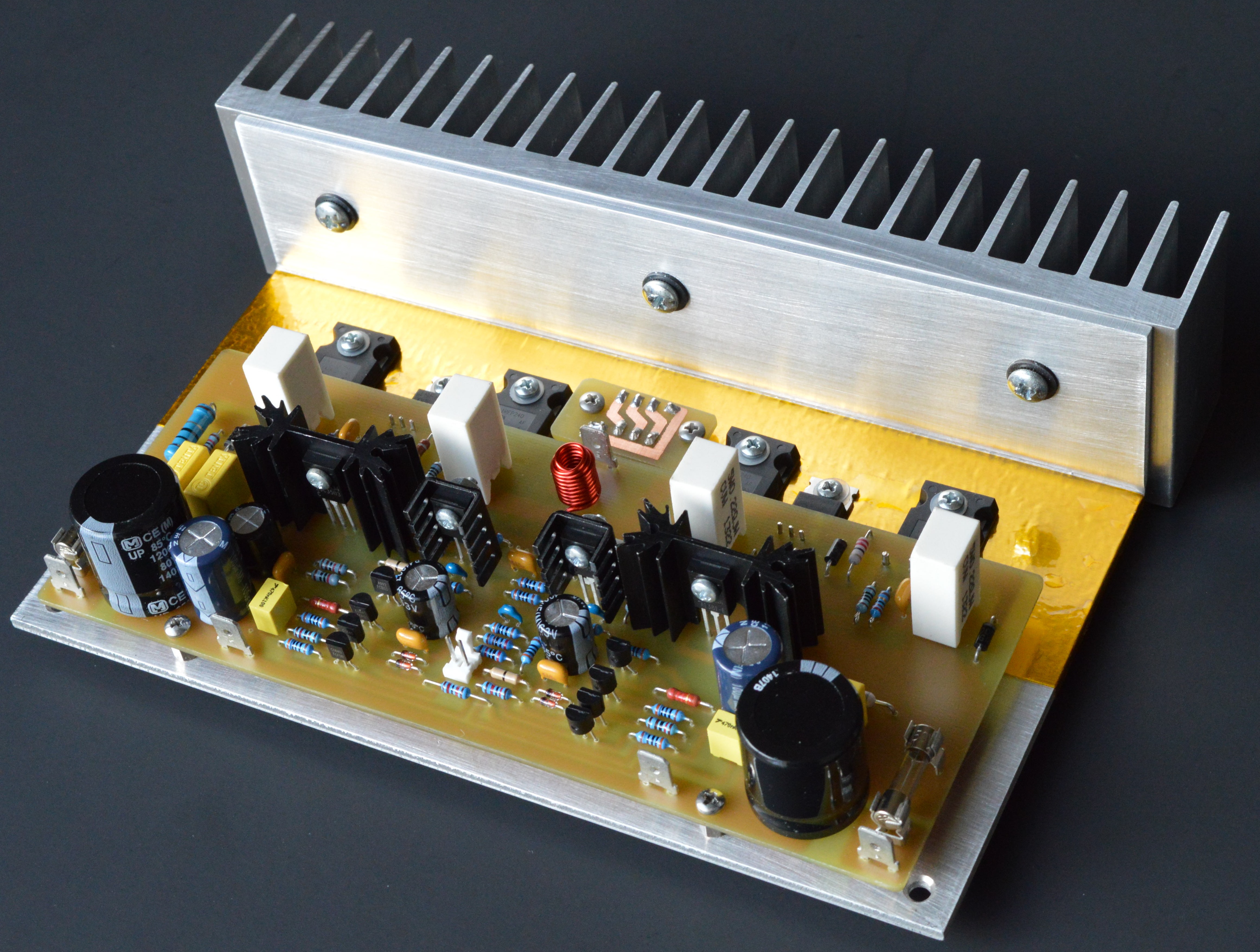
Project 60 is another version of The LeachAmp design utilizing power MOSFETs in the output stage. The quasi-complementary power output stage consists of TO247AC-packaged N-channel HEXFETs. The prototype was also tested with a TO3PN-packaged N-channel QFET from Fairchild Semiconductors. Although these vertical MOSFETs were designed primarily for high-speed switching applications and not for linear applications, both types performed satisfactorily in measured tests and during listening tests. The driver stage is also fitted with TO220-packaged N-channel and P-channel power MOSFETs.
The advantage of choosing vertical MOSFETs in a quasi-complementary output stage topology is cost and availability in comparison to lateral MOSFETs. At the time of this writing, an authentic IRFP240 will cost you less than a buck if purchased in quantities and is in stock at nearly all reputable online electronic parts vendors. However, the high performance audio lateral MOSFET from Exicon, SemeLAB or Renesas is perfect for this project as well, if not for its cost. If you are considering otherwise, please be aware with the package pin-out dissimilarity between vertical and lateral MOSFETs. As an example, a simple Hitachi-designed 100-watt lateral MOSFET project has already been presented in this website as Project 5.
When planning to develop a successful audio amplifier project, the most important goal to achieve is that the amplifier should be able to reproduce optimum audio quality. One of several ways to accomplish that goal is to use a front-end circuit that has been built, tested and proven to be a top-notch high performance design. This is what The LeachAmp is able to provide for this project. By using the superb front-end input circuit of “The LeachAmp” design, Project 60 is capable of reproducing excellent audio quality even though it uses a quasi-complementary output stage topology.
Here’s a caption of the statement from Dr. Leach’s website, “I have been asked why I did not use MOSFETs in the output stage. The main reason is that the original amplifier was designed with BJTs. Because a lot of great things have been said about MOSFETs, I did acquire a set of them, which I intended to develop an output stage with. I was disappointed to find these devices plagued with parasitic oscillation problems. The manufacturers recommend putting resistors in series with the gates and ferrite beads around the gate leads to suppress these oscillations. I found these methods to be only partially effective. Therefore, I temporarily abandoned the MOSFET output stage…” It’s sad to say that his MOSFET project was never realized (that I know of or I might be wrong) because of his passing in 2010. This project is a tribute to his exemplary contribution to the audio electronics field.
Project 60’s prototype was created using ExpressPCB, laser-printed and etched into a single sided 7.750” X 3.000” PCB. A smaller PCB was also created to mount all the diodes as part of the VBE multiplier circuit. This is connected to the main PCB by a pair of 22 AWG hook-up wires designated on the silkscreen top layer as “A” and “B”, and then mounted near the power transistors, as seen in the completed prototype pictures below. Solder another piece of 22AWG hook-up wire at locations labeled “X” to “X” on PCB, this allows the amplifier to be extremely quiet. Figure 1a shows the parts placement guide of a suggested PCB layout while Figure 1b shows a see-through top and bottom copper layer of the PCB for your convenience if you’re creating your own PCB with different CAD software. Project 60’s schematic diagram is found here and the BOM is found here.
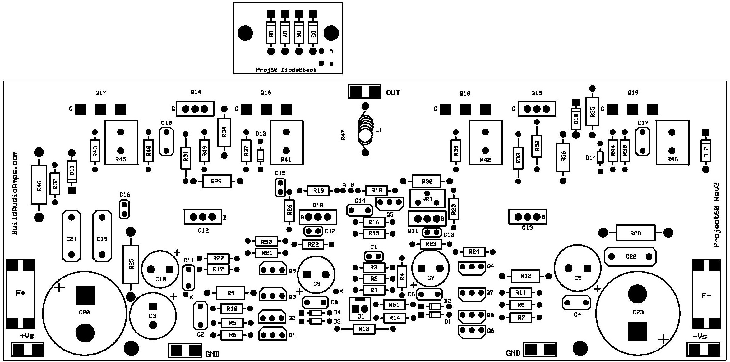
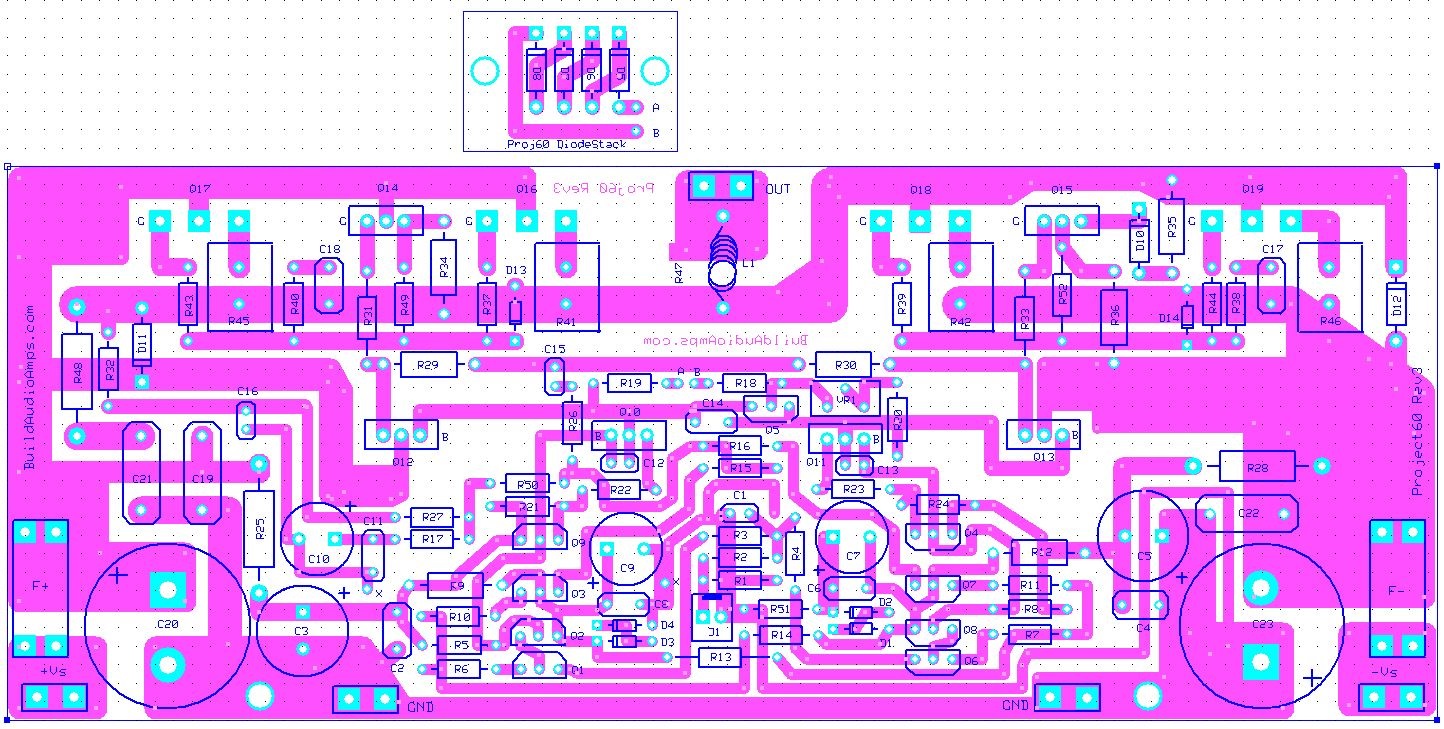
Figure 1a. Silkscreen, pads and text on top of the PCB. Figure 1b. A see-through top and bottom copper layer of the PCB.
The measured power output of the prototype is about 106 watts into an 8Ω load with ±50VDC to ±55VDC power supply rails. Less than 1Vrms of input signal is required to produce the full rated power output. The schematic diagram of Project 60 will be referred to from hereon. The original LeachAmp front-end circuit has not been modified for its application to this project, except for changes to the resistance values of R18, R19, R20 and VR1 in the VBE bias circuit. This increases the range of the output voltage of the VBE circuit, which is needed by the MOSFET devices. The gain (hFE) of all small signal transistors, Q1 through Q9, has been matched using a DMM with built-in hFE range at about 450. The transistor gain matching made the DC offset voltage of the amplifier to audiophile level as shown in Figure 2. D13 and D14 protect the gates of Q16 through Q19 from overvoltage or transients, while C18-R40 and C17-R38 prevents or damps out high-frequency oscillations. Another recommended method from IR is to insert a 5 to 10 ohms series resistor between the zener diode and the gate to prevent oscillations.
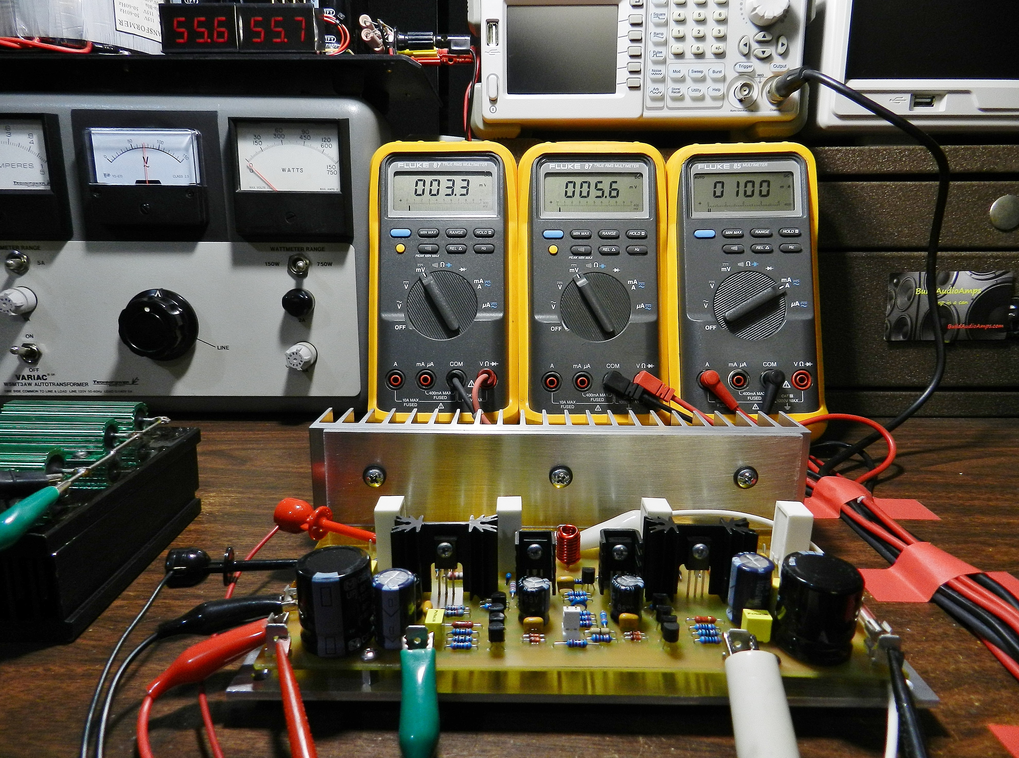
Figure 2. Initial test setup and measurements of Project 60’s prototype.
Figure 2 shows the initial test setup and results of the prototype. To avoid redundancy, if you have been reading BuildAudioAmps’ method of testing a newly built audio power amplifier module, it will not be mentioned again in how it got up to this point.
Before applying power to the amplifier adjust VR1 to maximum resistance, do not connect any load at the output of the amplifier. Install a shunt jumper at the input of the amplifier. The DC offset voltage of the amplifier is about 3.3 mV as shown in the DMM on the left. The typical DC offset voltage of the amplifier should be less than 50mV. The DMM in the middle is reading the voltage drop across any of the source resistors, R41 through R46 at 5.6 mV and this may be adjusted up to 20 mV depending on the builder. The 5.6 mV voltage drop across any source resistors is the minimum bias needed by the power transistors to reduce crossover distortion as observed during power output testing. The DMM on the right is connected across the F+ fuse terminals and measuring the total current drawn by the amplifier at 100 mA; this reading is dependent on the adjustment of VR1.
Alternately to determine the correct bias, a QA400 audio analyzer may be utilized for this purpose. Run a THD measurement and carefully adjust VR1 to get the lowest THD test result. This is as precise as you can ever get a low THD with the QA400 measurement, because the input test signal to the amplifier with a 1KHz center frequency is swept from the entire audio frequency spectrum.
You may proceed with the listening test if you have properly adjusted the bias of the power output transistors.
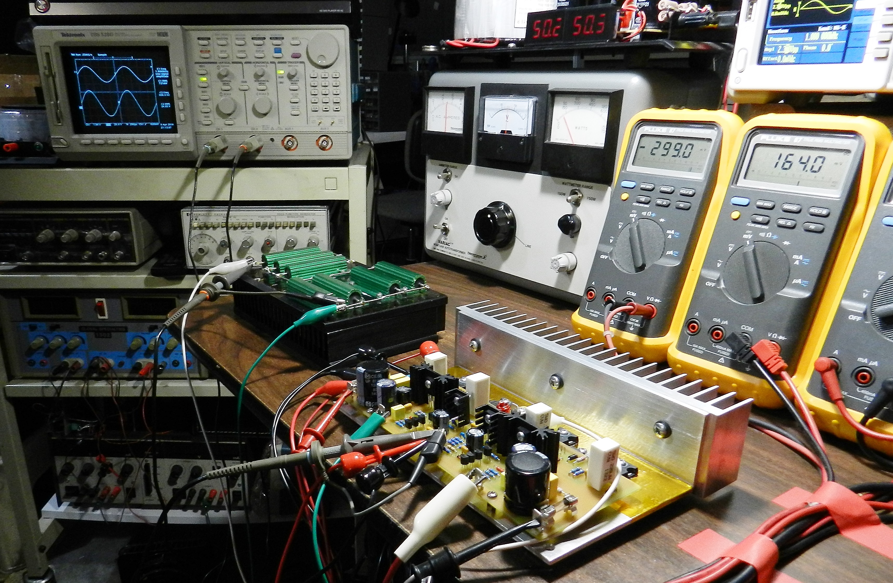
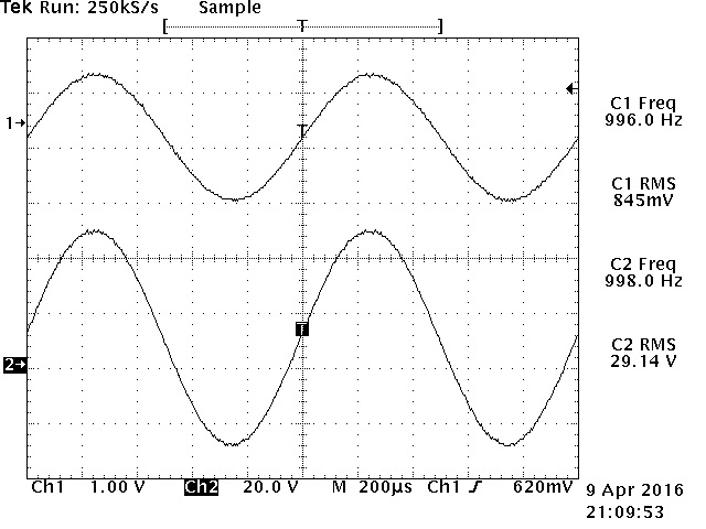
Figure 3. Power output and square wave test setup and measurements. Figure 4. Power output measurement test result of Project 60.
The next test procedure is optional. Figure 3 shows the test setup for power output and square wave response measurements. A 1KHz sine wave signal is applied to the input of the amplifier at J1. CH1 probe of the oscilloscope is also connected at J1. An 8Ω dummy load and the CH2 probe of the oscilloscope are connected at the output of the amplifier. Gradually adjust the amplitude of the input signal to about 845 mVrms while observing the output waveform in the oscilloscope just before clipping occurs. It may be necessary to adjust the variac transformer so that the voltage rails should be within the ±50 to ±55VDC range. Figure 4 shows a measured output waveform at 29.14 Vrms across the 8Ω dummy load; this is equal to a power output of 106.14 watts.
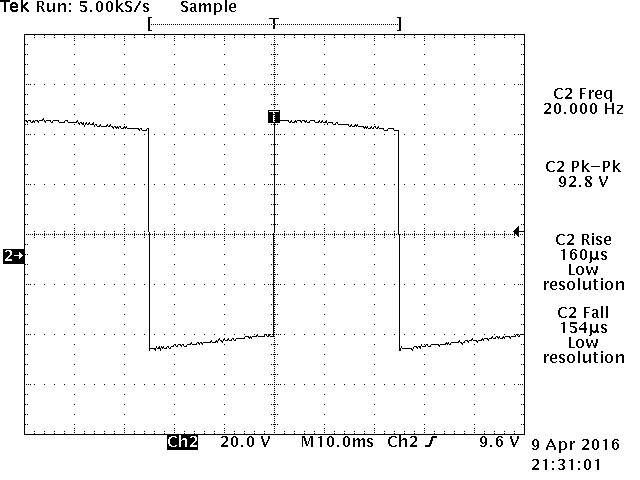
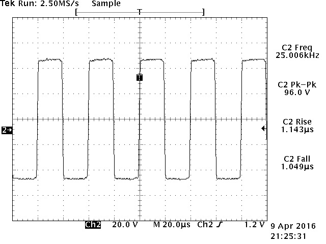
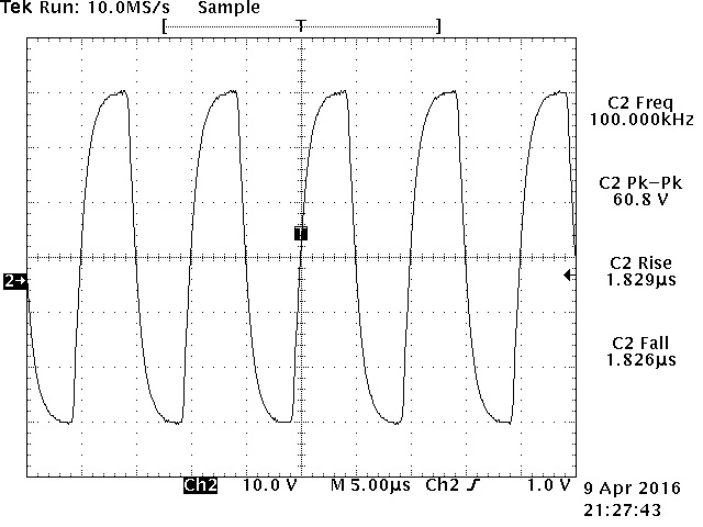
Figure 5. 20Hz square wave test result. Figure 6. 25KHz square wave test result. Figure 7. 100KHz square wave test result.
For the 100KHz square wave response testing, R48 should be removed from the output of the amplifier. Applying a continuous high frequency square wave signal to the amplifier will damage this resistor. Figure 5 shows the 20Hz square wave response with a slight amount of tilt. Figure 6 shows a very nice 25KHz square wave response while Figure 7 shows the 100KHz square wave response that is slightly rounded. Overall, there should be no ringing or overshoots on the output square wave signal as also mentioned in the Leach Amp Plans.
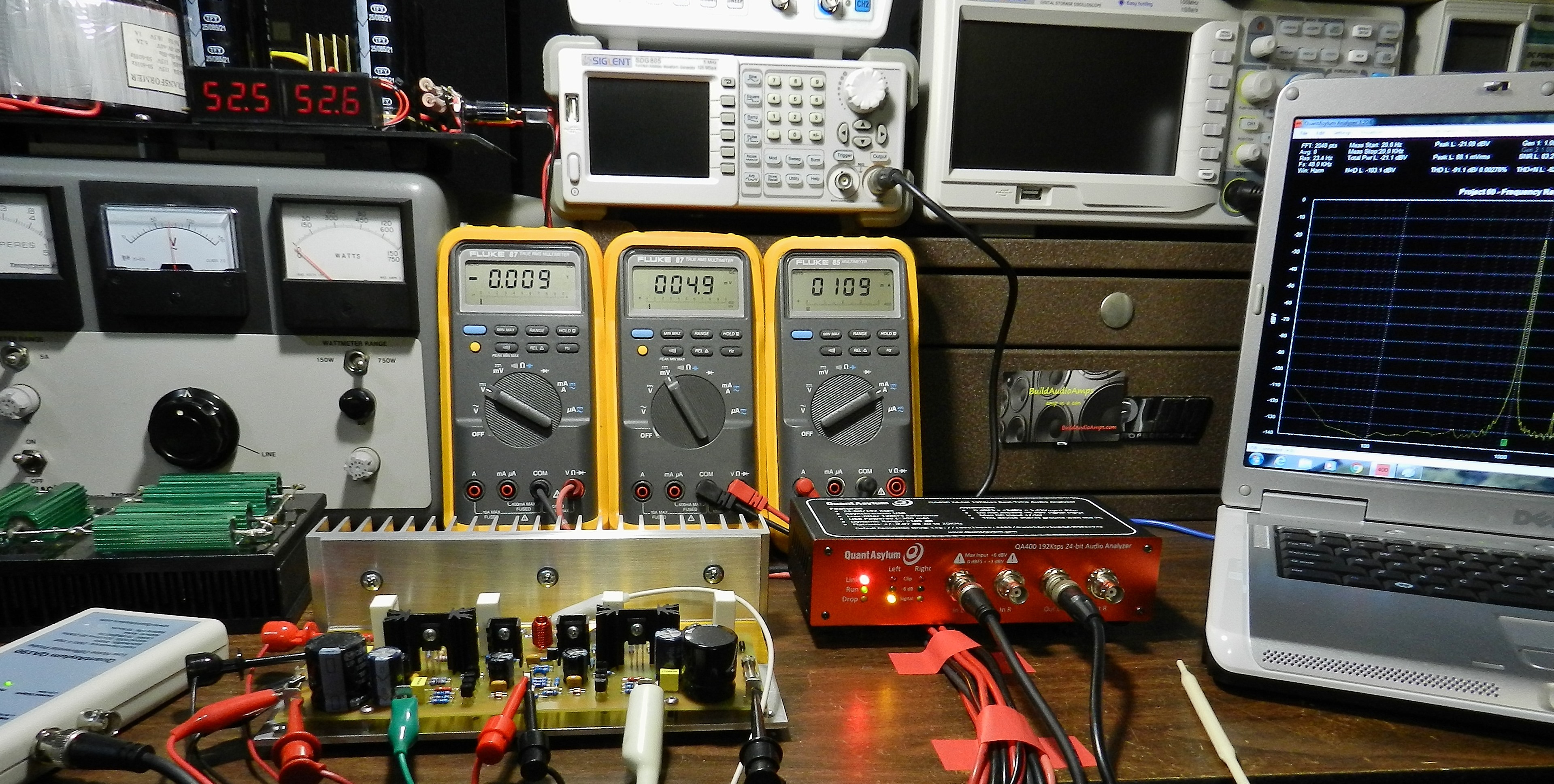
Figure 8. QA400 Audio Analyzer test setup.
Figure 8 shows a basic test setup of a QA400 audio analyzer. Allow the amplifier under test to warm-up for a few minutes before acquiring any test results. The audio analyzer test setup consists of a QuantAsylum’s QA400 USB audio analyzer, QA190 low-noise differential probe, 8Ω dummy load and a battery-powered laptop to measure noise, THD, THD+N, SNR and the frequency response of the amplifier. Figure 9 shows Noise, THD, THD+N and SNR test results while Figure 10 shows the frequency response test result. Also shown here is the Noise, THD, THD+N and SNR test results of the QFET, while the frequency response result is shown here.
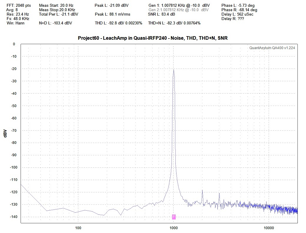
Figure 9. Noise, THD, THD+N and SNR QA400 test result.
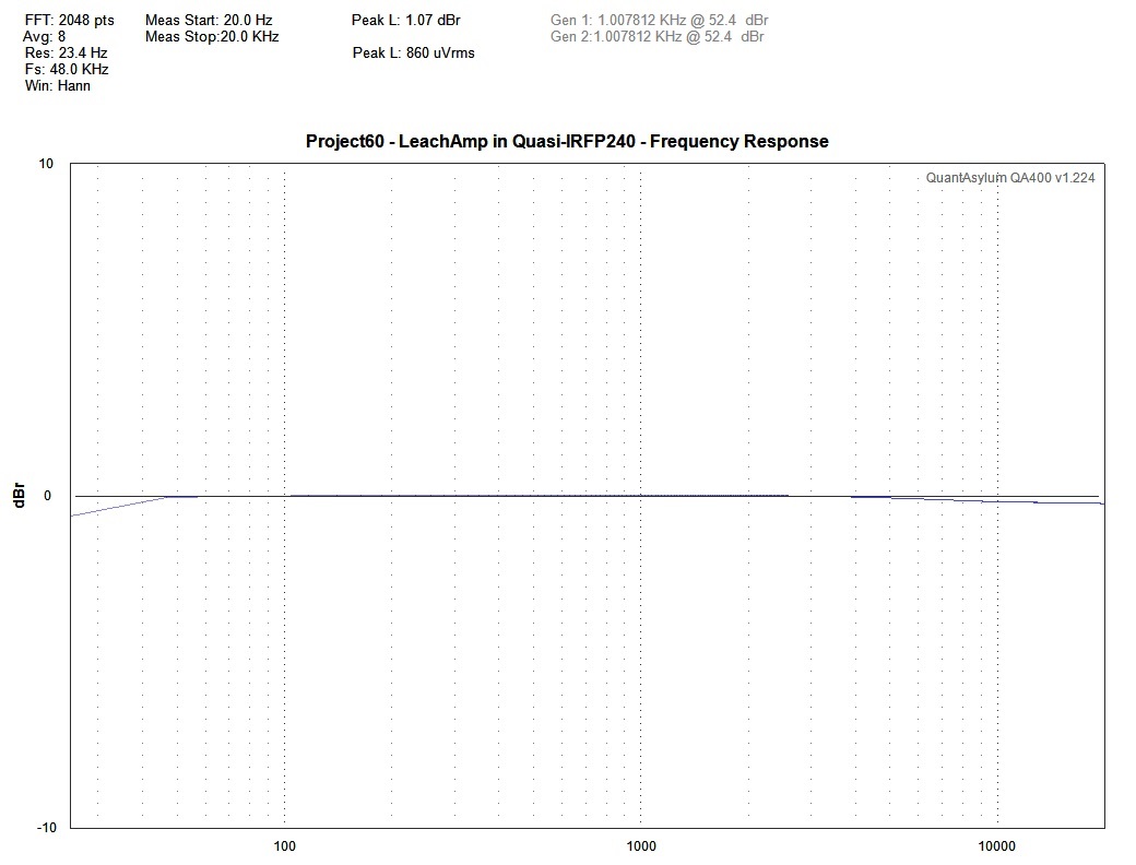
Figure 10. Frequency Response of Project 60 using a QA400.
How does Project 60 perform in music listening test? Listening to different CD album genres, the experience was impressive, although not as powerful as the previous Leach Amp project. The prototype unit was connected to a modified LM49720 tone control preamp, a Toshiba HD-A2 player, several test speakers and finally into a Bose Acoustimass 3 Speaker System with their inputs paralleled. In listening test both vertical MOSFETs, either HEXFET or QFET, have their own tone character. The QFET has noticeably more sibilance especially on the percussionist’s snare drum, cymbals and on the hi-hat than when compared to the HEXFET. The HEXFET has a more balanced tone, that is, equally reproduced lows, mids and highs. But then again this is subjective in nature and you may perceive differences in listening, given a different set of music signal sources and speaker loads. But the overall build experience of the project did not disappoint.