Project 65


Project 65 is the fourth in the series of audio power amplifier projects that uses an op-amp in the front-end stage of the amplifier. The CFA-based op-amp input stage is connected to a full complementary hybrid compound feedback pair output stage. The implementation of BJT drivers and MOSFET power output devices is sometimes referred to as a hybrid design. The schematic diagram of this amplifier is similar to the Alexander CFA power amplifier and Exicon MOSFET’s application notes. The schematic diagram of this project is found here.
Without the voltage feedback network in the op-amp circuit as implemented in an earlier project, there is the need of adjusting the DC offset of the amplifier. Prior to deciding the inclusion of a null offset trim circuit to the project, at power-up the DC offset output of the amplifier is about 200mV. In the Alexander amp it uses an integrator circuit to automatically minimize the DC offset voltage similar to the circuit implemented in Project 4. However, in this project a fixed resistor and a multiturn trimmer potentiometer were added to set the overall DC offset of the amplifier to minimum. Although this approach is simpler than using an integrator circuit, it does have a disadvantage of drifting as temperature rises but within acceptable level. The next decision then is to choose an op-amp with a low offset drift. Generally, bipolar op-amps have very low temperature drift, but the JFET-input op-amp chosen for this project has a temperature coefficient of input offset voltage or drift at ±3.2uV/°C. Does it affect the audio quality of the amplifier? Because this is a CFA-based amplifier with a CFP output stage, it’s hardly noticeable in the listening test; the drift issue does not in any way color the audio quality of the amplifier. The amplifier sounded powerful enough even though it puts out less than 200watts into an 8Ω load.
Some op-amp manufacturers do not recommend using this approach. “The internal adjustment terminals should therefore be used only to adjust the op amp's own offset, not to correct any system offset errors, since doing so would be at the expense of increased temperature drift. The drift penalty for a FET input op amp is in the order of 4 µV/°C for each millivolt of nulled offset voltage. It is generally better to control offset voltage by proper device/grade selection.” –taken from Analog Devices MT-037, a tutorial on op-amp input offset voltage. This is true if the op-amp is used in special instrumentation applications where DC precision and accuracy is a requirement, however it works just fine in this project. I may be wrong, but I have not yet found an audio power amplifier circuit similar to what is implemented in this project –using the op-amp’s internal offset trim circuit to control the overall DC offset of the amplifier.
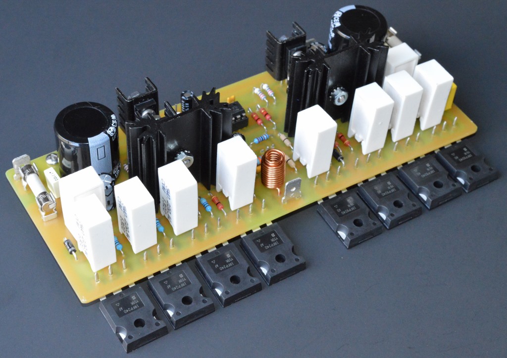
Applying a 1KHz 1.84Vpp input signal, the amplifier produces 35.82Vrms across an 8Ω load when connected to a ±56.6VDC power supply rails and a THD of 0.002%. Higher power output may be realized if connected to low impedance loads. The overall gain of the amplifier is 23 or 27.2dB, determined by using equation 1 found in the Alexander amp’s plans. Revision 2 of the project increases the value of resistor R3, part of the negative feedback network, to reflect to this gain and fixes instability issues common to CFP topology. There is no protection circuitry included in the project, however the uPC1237 Speaker Protection and Power ON Delay Project could easily be added for peace of mind. The project’s prototype was created using ExpressPCB, laser-printed and etched into a 7.000” X 2.750” single-sided copper board.
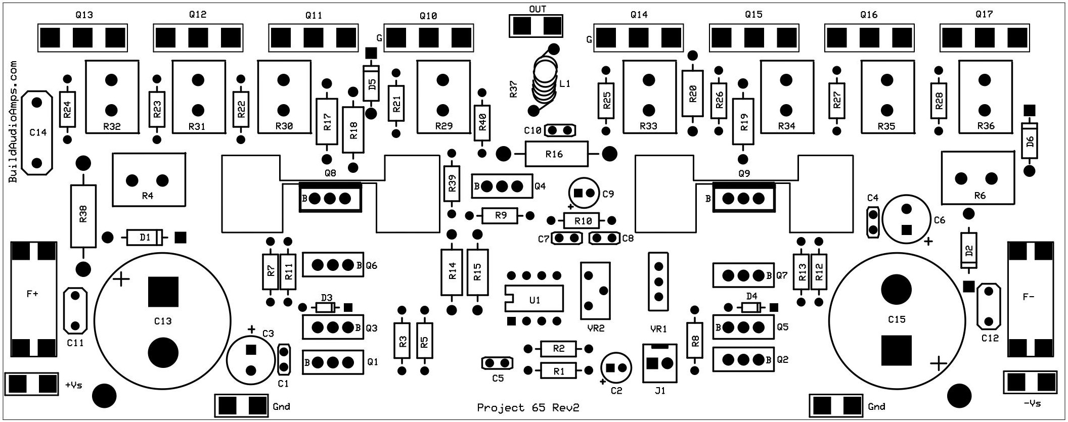
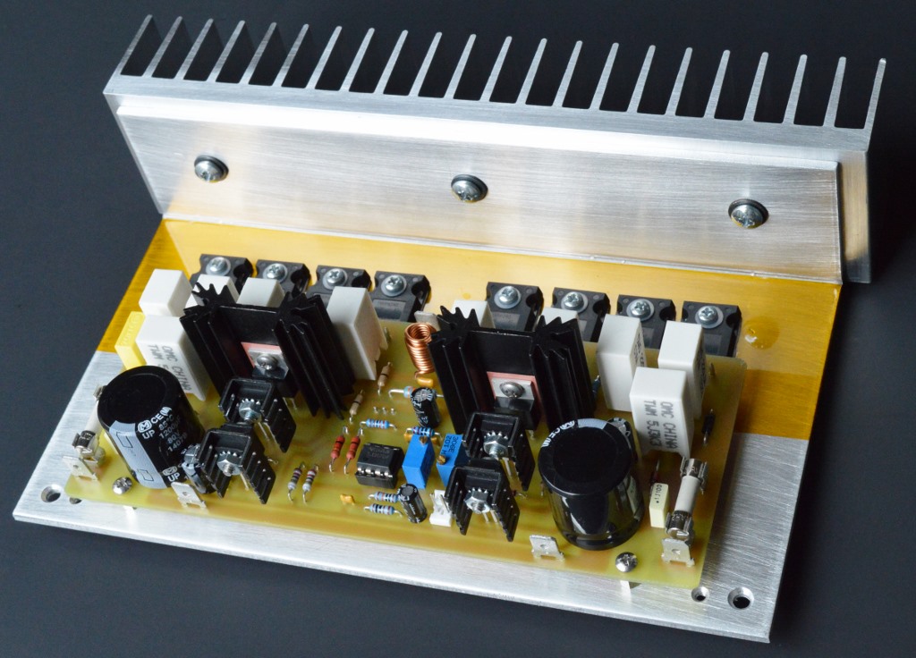
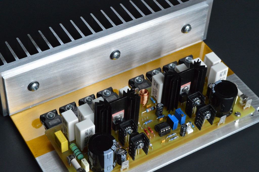
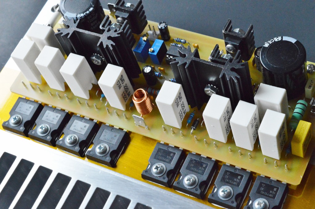
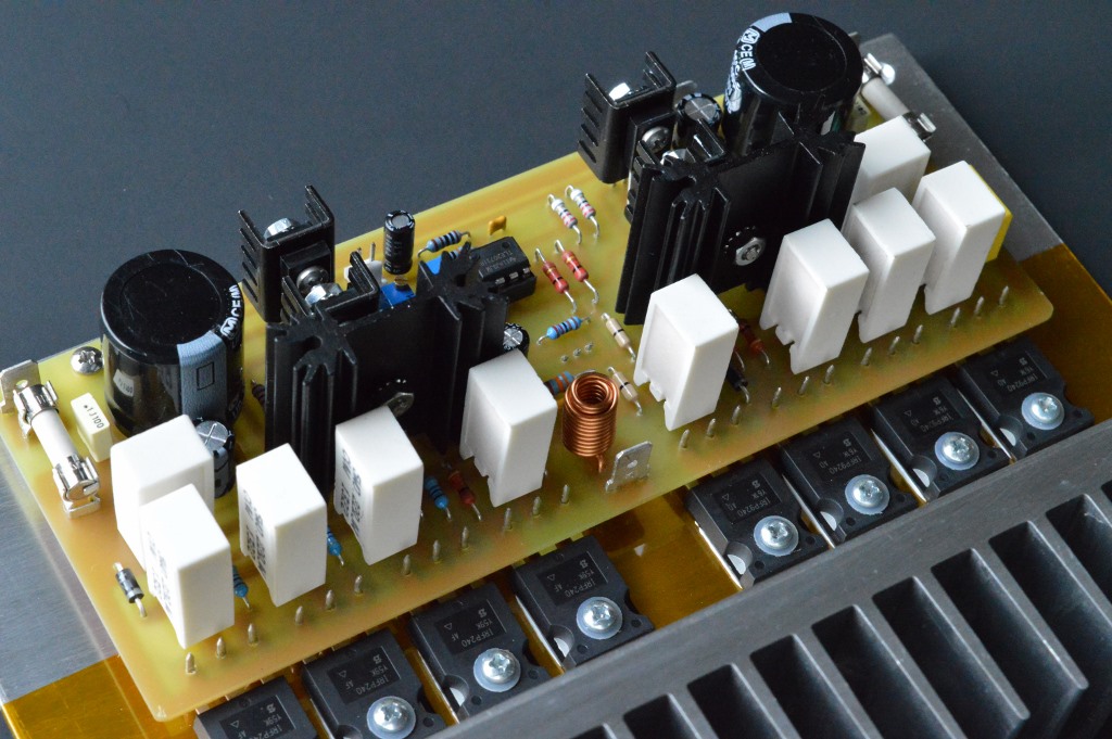
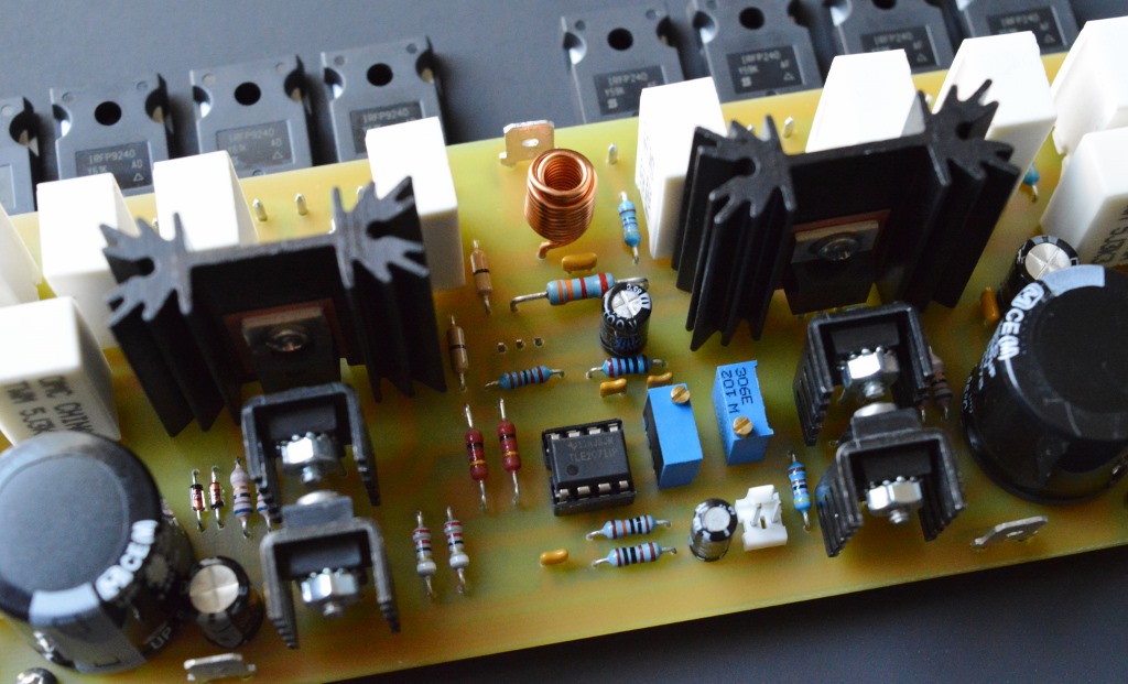
Figure 1. Project 65 parts placement top layer of PCB.
A suggested initial test setup of the project is shown in Figure 2 using several DMMs and a test dual polarity power supply connected to a variac power transformer. The project may be connected to ±55VDC to ±57VDC power supply rails. These are obtained from a rectified and filtered 38VAC-0-38VAC or 40VAC-0-40VAC toroidal power transformer similar to AnTek P/N AS-4438-400VA 38V or P/N AS-3440-300VA 40V transformer, respectively. Adjust VR2 to maximum resistance before powering up the amplifier. Leave VR1 as is at this time. Do not connect any input signal or load at the output of the amplifer. If the power MOSFETs are attached and secured into a heat sink make sure to check the infinite resistance between all the drain terminals and heat sink.
Please refer to Figure 2. The test power supply output voltage is about ±57VDC. The ambient workshop temperature is about 90°F, on a typical summertime in SW Texas. The DMM on the left is connected to the output of the amplifier. This measures the DC offset voltage of the amplifier at 0.5mV. This was acquired by adjusting VR1 after a warm-up period of 15 minutes or more. The DMM in the middle is connected across R36 or any of the drain resistors of the power MOSFETs. The DMM measures 4.7mV and this could be anywhere from 3mV to 10mV. Carefully adjust VR2 after the warm-up period to acquire the suggested voltage drop across the drain resistor. The DMM on the right is measuring about 146mA, which is the total current drawn by the amplifier. This DMM is connected across the F+ fuse terminals, of course with the fuse removed. If you have only one DMM available you can connect it this way to measure the total current drawn by the amplifier at about 146mA. This reading is dependent on the adjustment of VR2.
If you have adjusted the amplifier similarly, you may proceed to listening test. If not you may continue with the optional power output, square wave response and QA400 audio analyzer tests, if the test equipments are available.
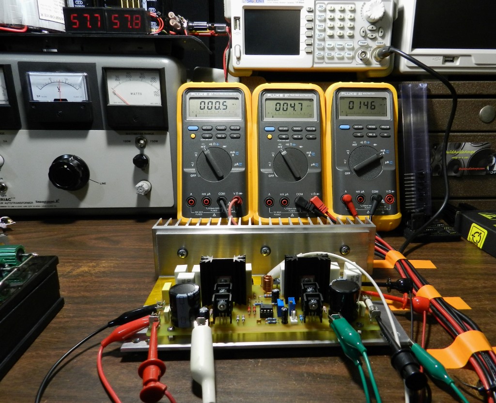
Figure 2. Initial test setup of Project 65.
Figure 3 shows the test setup for power output and square wave response tests. An oscilloscope, function generator and an 8Ω dummy load are required for the test. In the power output measurement, the function generator is set for a sine wave output at 1KHz and its amplitude is adjusted initially at 100mVp-p. This test signal is connected to J1 of the amplifier as well as CH1 of the oscilloscope. An 8Ω dummy load and CH2 of the oscilloscope are connected to the output of the amplifier under test. Figure 4 shows a hardcopy of the test result with Rev1 of the prototype. At 1KHz 1.84Vp-p the amplifier produces 35.82Vrms across the 8Ω dummy load. This is equal to a power output of 160.38watts. It was mentioned earlier that the value of resistor R3 was increased in Rev2. Therefore the amplitude of the 1KHz input signal at CH1 should be higher than what is shown in Figure 4, however the output amplitude would still be attainable without clipping.
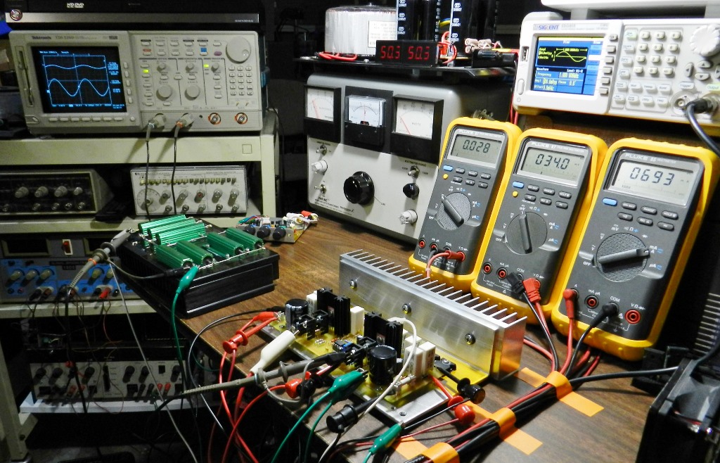
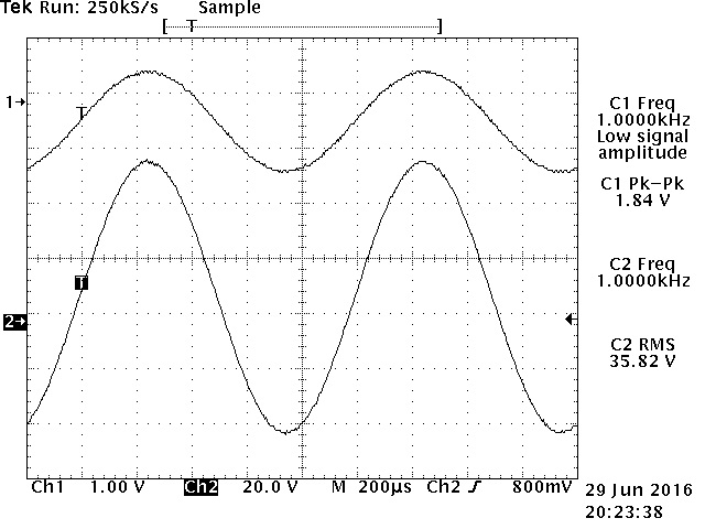
Figure 3. Power output and square wave response test setup. Figure 4. Hardcopy test result of power output test.
Several square wave frequencies were selected to show how the amplifier would respond and amplify these signals. Figure 5a through 5d shows the test results for 20Hz, 1KHz, 20KHz and 100KHz square wave test signals. While it is possible to increase the amplitude of the square wave test signal before displaying overshoots, it was however adjusted marginally for safety reasons. The test results, simply put, are representations of how the amplifier will behave for a given square wave frequency. Although, it was observed in the tests that the 1KHz sine wave test signal was more unforgiving when its amplitude was increased, which made the amplifier become unstable and oscillate at more than its rated power output. However, in real world conditions, this was hard to replicate with actual music input signals.
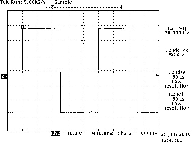
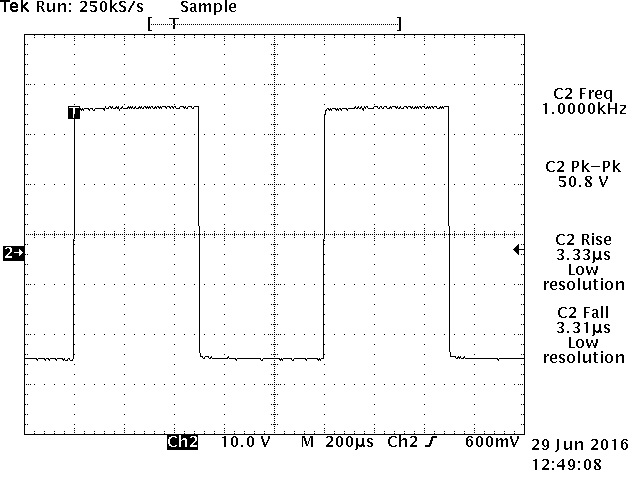
Figure 5a. 20Hz square wave response test. Figure 5b. 1KHz square wave response test.
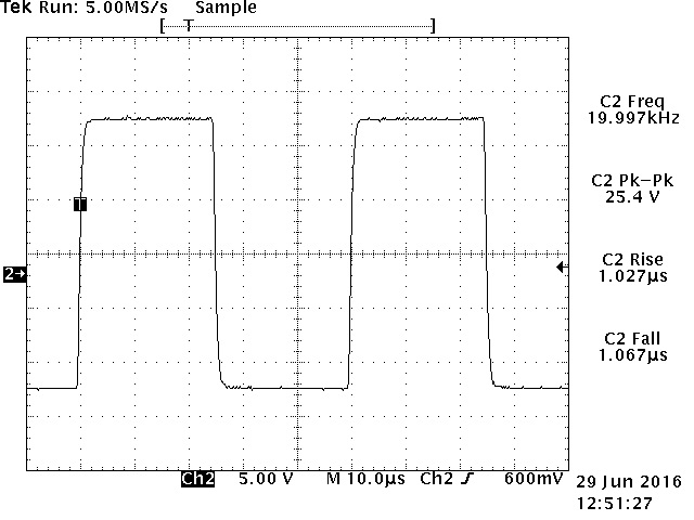
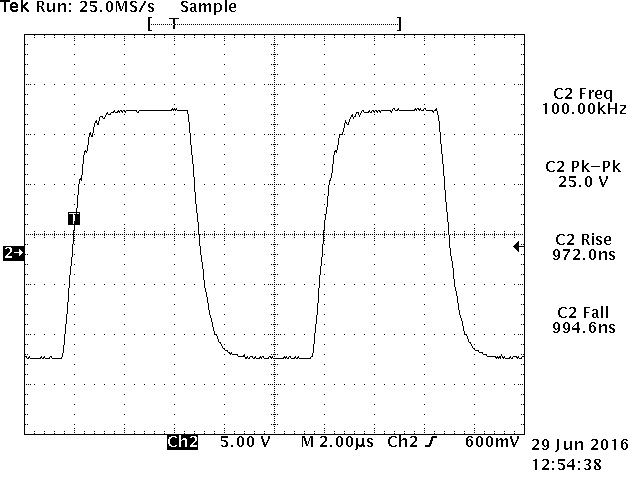
Figure 5c. 20KHz square wave response test. Figure 5d. 100KHz square wave response test.
Figure 6 shows QuantAsylum’s QA400 audio analyzer with the QA190 differential probe test setup. The left or right channel signal generator output of the QA400 is directly connected to the input of the amplifier under test. Depending on the type of measurement, the signal generator generally generates a 1KHz sine wave signal at -10dB with a sweep span from a start frequency of 20Hz to a stop frequency of 20KHz; however, all these values are user definable. Although QuantAsylum have released their second generation of audio analyzer, the QA400 will suffice at this time to show the measured performance of the built audio amplifier project. The test results are shown in Figures 7a and 7b.
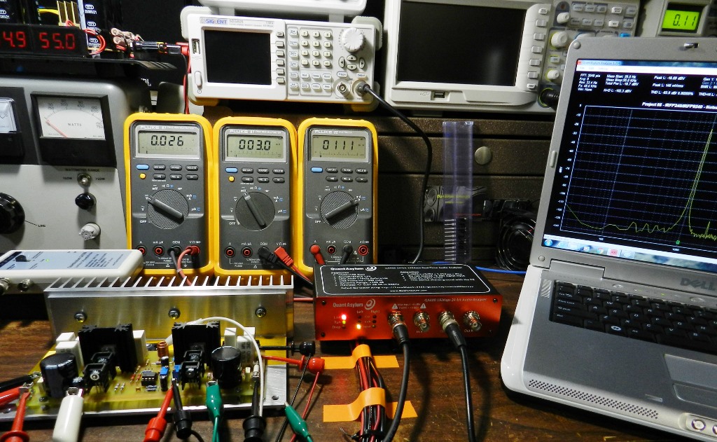
Figure 6. QA400 test setup for Noise, THD, THD+N and SNR.
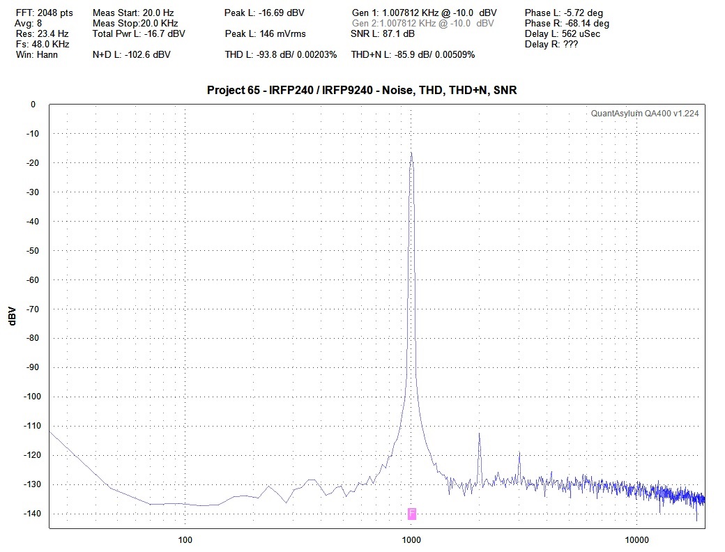
Figure 7a. QA400 test result for Noise, THD, THD+N and SNR of Project 65.
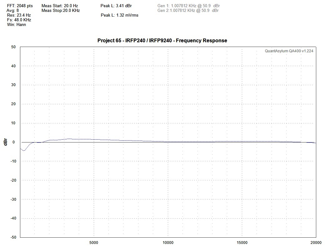
Figure 7b. QA400 test result for Frequency Response of Project 65.
How does this project sound? If you have built a similar CFP-based amplifier project, then you will agree that the audio quality this type of output stage will reproduce is very much impressive. The prototype unit was connected to a modified LM49720 tone control preamp, Toshiba HD-A2 player and several test speakers. While playing tracks 2 and 13 of Monty Alexander’s “Stir it up” album, you hear deep bass, pleasing mids and extended highs. With the same setup and this time for endurance music testing, the entireties of SafriDuo’s “Episode II” and Gabrielle Roth’s “Tribe” albums were auditioned. Several CDs of different genres were also played for the listening test.