Project 24
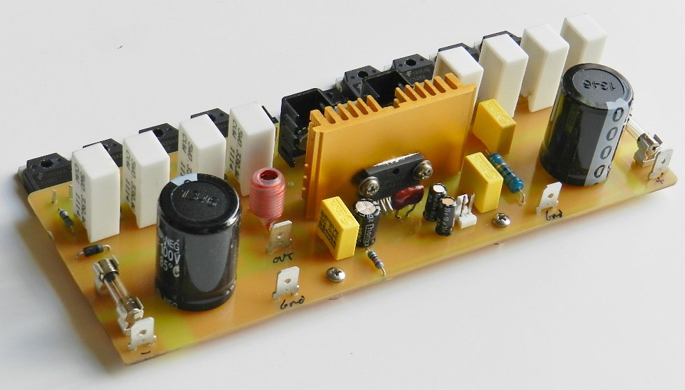
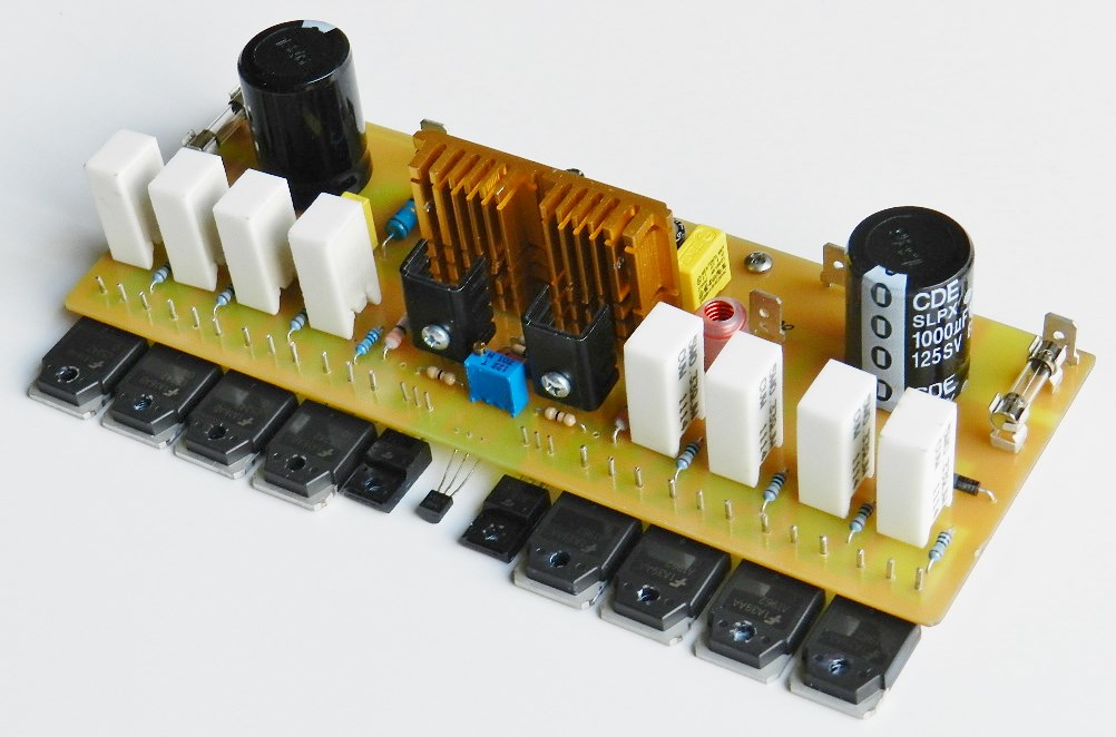
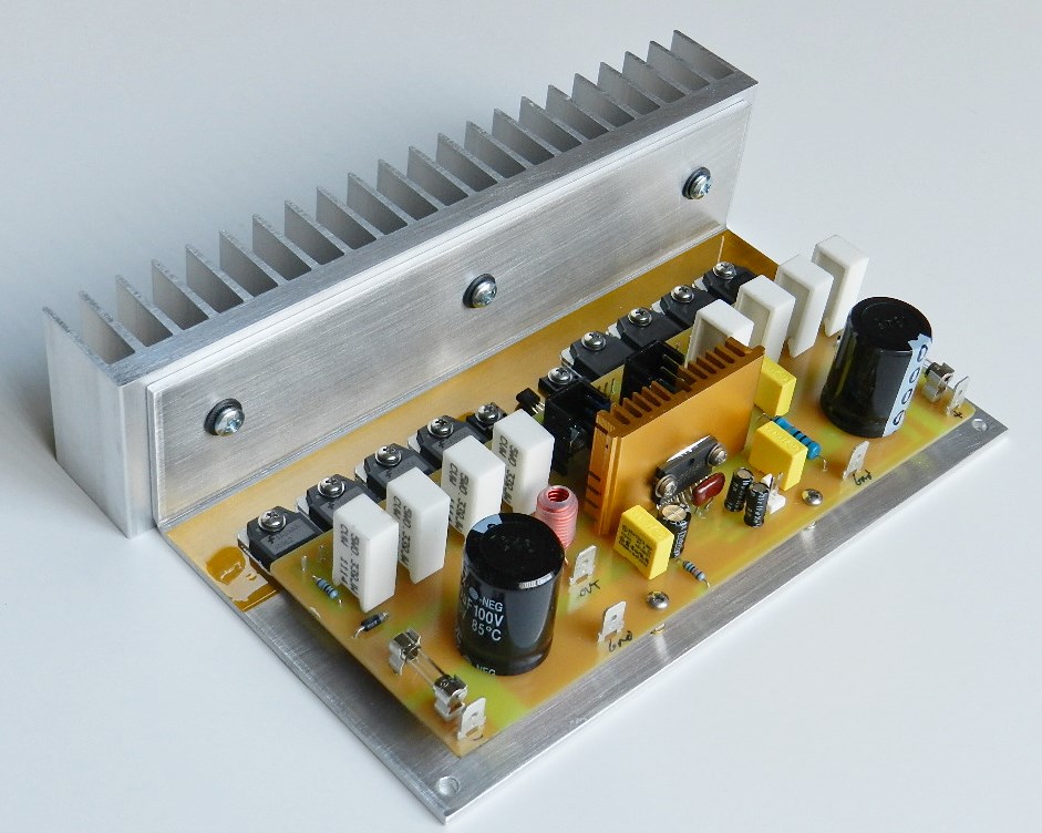
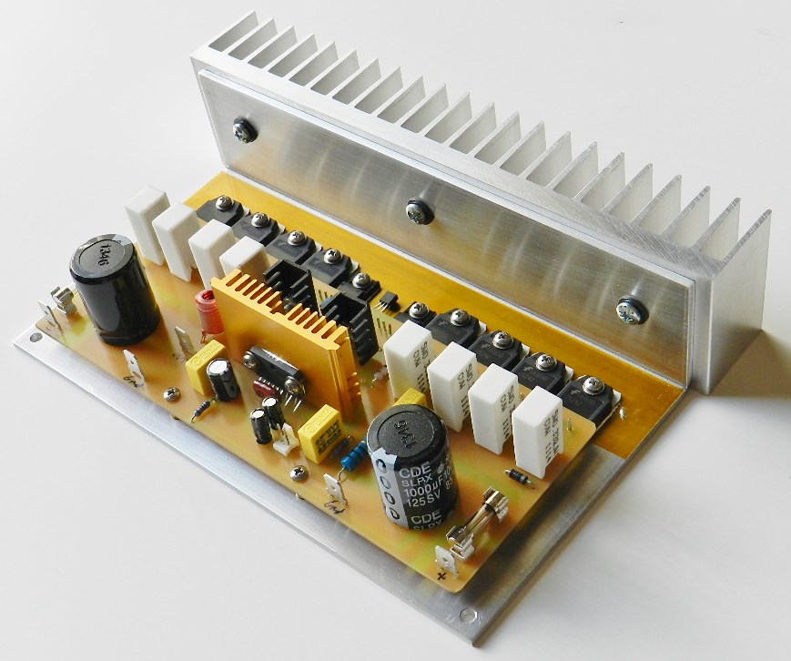
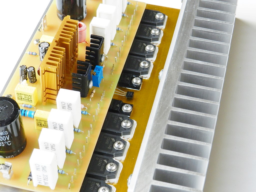
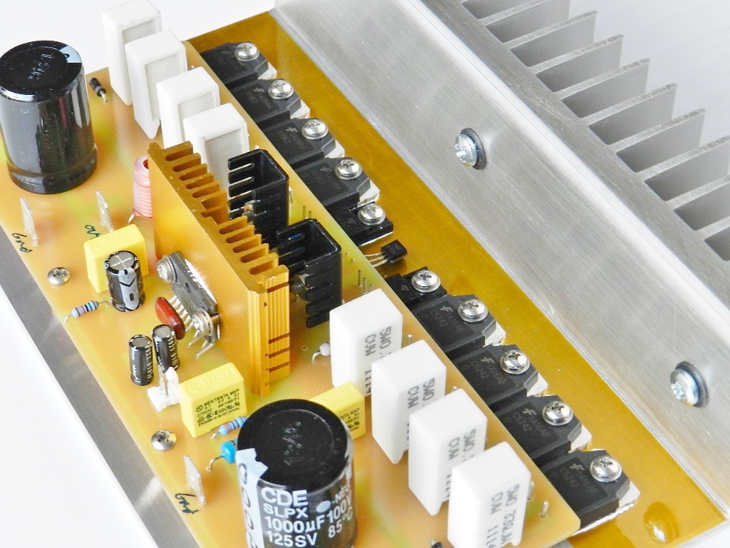
Project 24 is another LME49811 power amplifier project. The LME49811 input stage drives a three-stage emitter-follower output stage. The first driver stage, Q2 and Q8, uses a single shared emitter resistor, R21. This stage also buffers the LME49811 outputs from the second driver stage. C11 and C12 were added at Q2 and Q8 for high frequency compensation and improve overall stability of the amplifier. The second driver stage, Q3 and Q9, uses separate emitter resistors, R22 and R25, which are connected to the main output bus of the amplifier. The output of the second driver stage drives four pairs of complementary TO-3P packaged power output transistors, Q4 thru Q7 and Q10 thru Q13. The power output of Project 24 was measured at 260Wrms into an 8Ω load or 520Wrms for 4Ω load with a ±70VDC up to ±75VDC power supply.
The project’s PCB uses a mixed of SMD components around the LME49811 and Through-Hole components on the power output stage. The schematic diagrams, BOM and PCB layout for Project 24 are available for free by request, as is, no warranty.
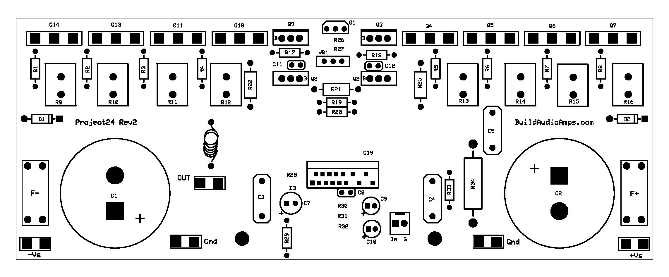 Project 24 Silkscreen parts placement layer of PCB.
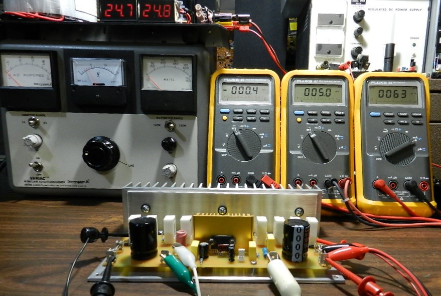
A word of caution if you intend to build this project: Project 24 uses high power supply voltage rails, please pay attention and be very careful not to touch any component while the amplifier under test is powered-up at maximum, you will get an electric shock and will result in serious injury if accidentally touched! A safe way of powering up your newly built project for the very first time is to use a ±24VDC power supply or whatever low voltage dual power supply that you may have.
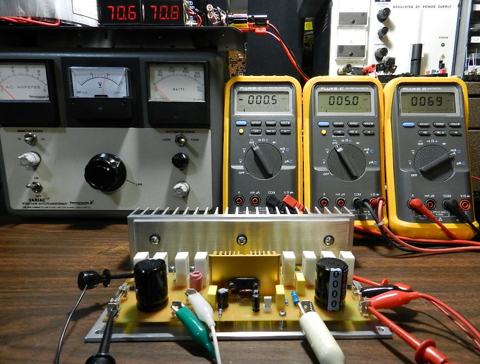
Insert a jumper or shunt at the input of the amplifier. Do not connect any load or loudspeaker at the output of the amplifier. Prepare 3 DMMs to measure the DC offset voltage, the voltage between the emitters of Q7 and Q13 power output transistors and the current across the F+ fuse terminals.
The picture on the left with a ±24VDC power supply shows the DC offset voltage at 0.4mV measured at the output of the amplifier, 5mV across the emitters of Q7 and Q13 and the current measured across the F+ fuse terminals at 63mA. Carefully adjust VR1 to obtain the 5mV reading after a warm-up period of about 10 minutes. If you get different DMM readings, switch the power supply to OFF immediately and check for PCB assembly errors. If you intend to power the project at this voltage level you may do so, the music fidelity it reproduced, in my opinion, is still very pleasing and does not disappoint!
If a Variac transformer is available, connect the AC input of the power supply to the output of the Variac transformer. Switch the power to ON and gradually adjust the Variac’s AC output voltage from zero until the voltage output of the power supply reaches ±70VDC while keeping an eye on sudden increase in any DMM readings. If you have observed an increase in any of the DMM readings, try adjusting VR1 if it decreases the DMM readings, if not switch the power to OFF immediately and check the PCB for assembly errors. The picture on the right with a ±70VDC power supply shows a very good DC offset voltage at 0.5mV, the voltage across Q7 and Q13 at 5mV and the current across the F+ fuse terminals at 69mA. Readjust VR1 to get the 5mV reading after 10 minutes, after that, you may proceed with music test!
If a Variac transformer is unavailable, make sure that the power supply has been properly built and that the output voltage rails have been measured at ±70VDC before connecting it to the project. With the power supply at OFF, adjust VR1 for minimum resistance. Switch the power supply to ON; the DMM measuring the voltage across Q7 and Q13 should read less than 1mV. If the DMM reading is more than 1mV and cannot be adjusted, power OFF immediately and check the PCB for assembly errors. If the DMM reading is less than 1mV, wait for 10 minutes for the bias to stabilize and then carefully adjust the reading to 5mV, after that, you may proceed with music test!

The next test procedure is optional, but if an oscilloscope, audio signal generator and 8Ω dummy load are available, the maximum power output before clipping occurs can be measured. Be extra careful not to touch the heat sink or the dummy load during this test, they will get extremely hot (you can smell it)! After building Project 21, I’ve improved the dummy load’s heat sink and added more series-parallel connected power resistors for a total resistance of 8Ω and a combined power rating of 700watts.
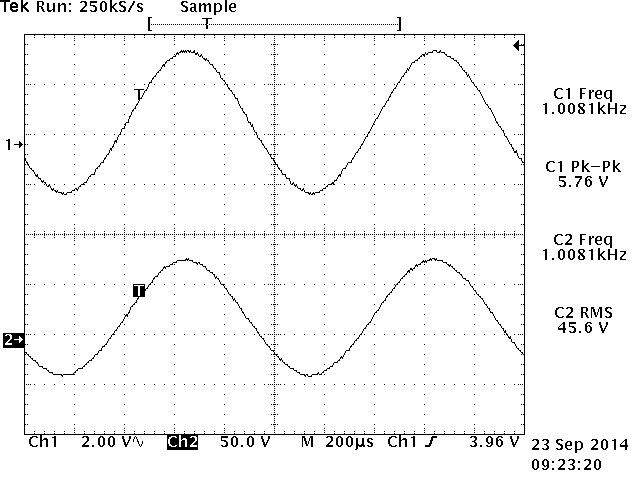
The power output was measured using an HP3312A Function Generator set at 1KHz 5.76Vp-p sine wave output and connected directly to the input of the amplifier under test as well as the CH1 test probe of the oscilloscope. An 8Ω/700Watt dummy load was connected at the output of the amplifier under test as well as the CH2 test probe of the Tektronix TDS520D 500MHz Digital Phosphor Oscilloscope. The amplifier produces 45.6Vrms across the 8Ω/700W dummy load or a power output of about 260Wrms, as shown in the TEK hardcopy picture on the right. The oscilloscope’s horizontal scale was adjusted at 200uS to verify for any visible clipping or artifacts on either peak.
A forced air-cooling is required for this project for long-term reliable performance. The model unit was supplied with a ±80VDC, a 1KHz input signal and an 8Ω load for a few minutes and survived, but not recommended unless modifications are made. This project was paired with Project 9, the LM1036 tone control project.