Project 46

Introduction. Project 46 was inspired by a Current Feedback Amplifier (CFA) project developed by www.andiha.no. Thanks to Knut Harald Nygaard for allowing BuildAudioAmps to present his excellent CFA-based audio power amplifier design. The project is rated at 25 watts at 8Ω operating in Class A mode. The schematic diagram, theory of operation, assembly and test procedure are well explained in his website.
Current feedback amplifiers have faster slew rate, wider bandwidth, more clarity and broader separation of the musical audio spectrum. With those remarkable characteristics, choosing either Class A or Class A/B mode of operation, seems not to matter since there’s barely enough perceivable difference between the audio fidelity that both classes will reproduce. Having said that, Project 46 will operate at a much cooler and more efficient Class A/B mode with no degradation to its audio quality. Nevertheless, we will just leave it up to the amp builder to decide!
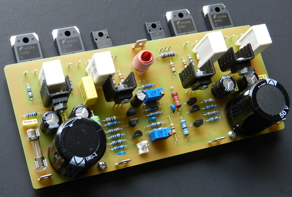
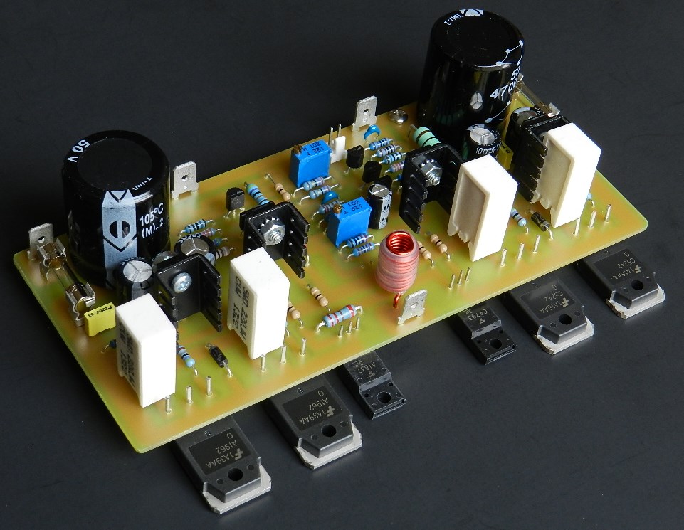
Changes made. Please refer to Project 46’s schematic diagram from hereon. The recommended JFETs, Toshiba’s original part numbers 2SK170/2SJ74, unfortunately have discontinued or obsolete lifecycle status. Knut on the other hand suggested that these JFETs have available replacements at Linear Systems as LSK170 and LSJ74. It was not tested on this project, but rather, different JFETs from Fairchild Semiconductor were used. The addition of cascode transistors to these JFETs allows a safe source to drain voltage at approximately 13VDC.
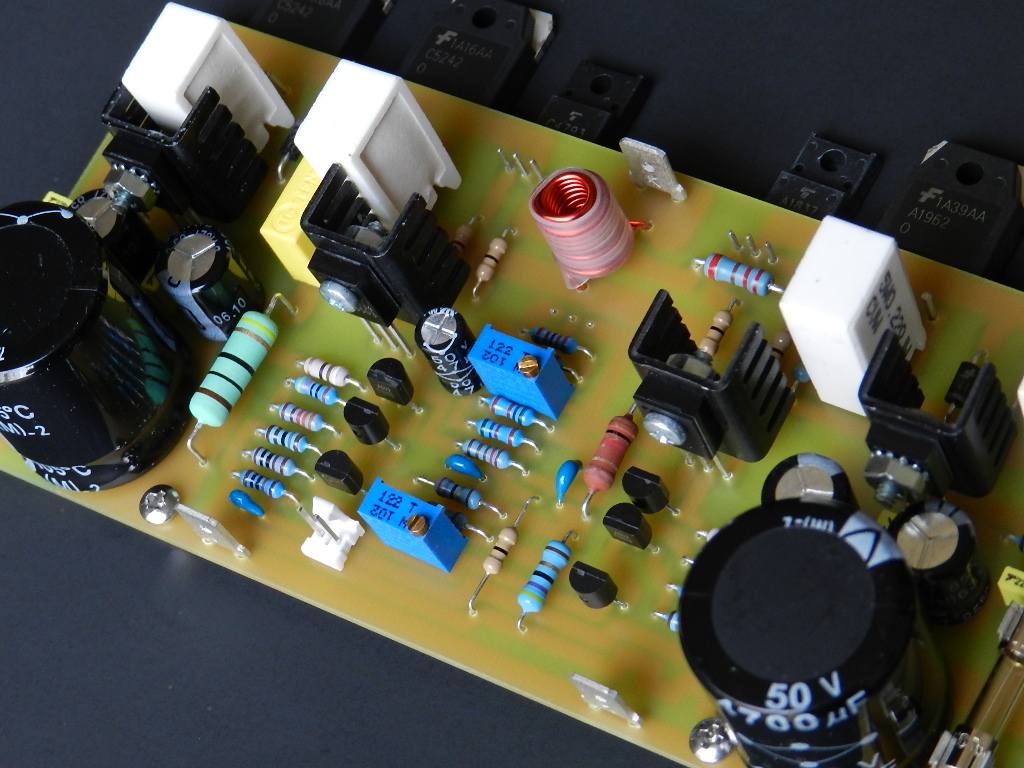
The common node point where all the negative feedback resistors, DC offset trim potentiometer and compensating capacitors are connected together has to be modified. Without any changes to the original circuit, the DC offset voltage was unacceptable. However, with the addition of source resistors, R9 and R10, in parallel with VR1, the DC offset voltage can now be adjusted anywhere within ±100mV.
An Aavid Thermalloy P/N 575200B00000G heatsink clip was installed to the TO92-packaged transistors, Q3 through Q6. This heatsink reduces DC offset voltage settling time caused by the change in case temperature of these transistors.
The recommended 4700uFd decoupling capacitors required by the input stage were replaced with positive and negative capacitance multiplier transistors, Q9 and Q10. These were populated to substitute the 22Ω resistors used in the original circuit. The capacitance multipliers are basically emitter-follower circuits that multiply the capacitance values of C7 and C9 by its current gain (β). A voltage drop of approximately 1.4VDC is developed across each transistor. The modification beneficially reduces the footprint of the PCB.
No changes were made to the double emitter-follower power output stage circuit, except that it’s now operating in Class A/B mode. Two pairs of paralleled complementary TO3P power transistors were added to handle the increase in the power supply rails at ±35VDC or ±45VDC, whichever you prefer. The DC supply rails are produced from a rectified and filtered 50VCT or 64VCT at 200 or 300VA power transformer. The bias for the power output stage transistors can be set at 90mA per transistor pair or higher. This is where you decide as to how the amplifier will operate either Class A or Class A/B mode. Increasing the bias of the power output stage transistors allows the amplifier to operate in a Class A mode. If you choose to reduce the quiescent current as in Class A/B mode, the operating temperature of the amplifier will also decrease. The measured power output of this project before clipping is 55 watts at 8Ω or 110 watts at 4Ω.
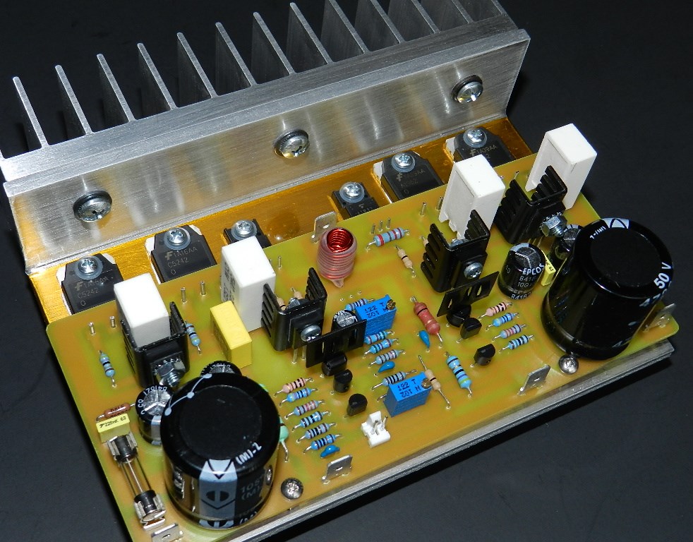
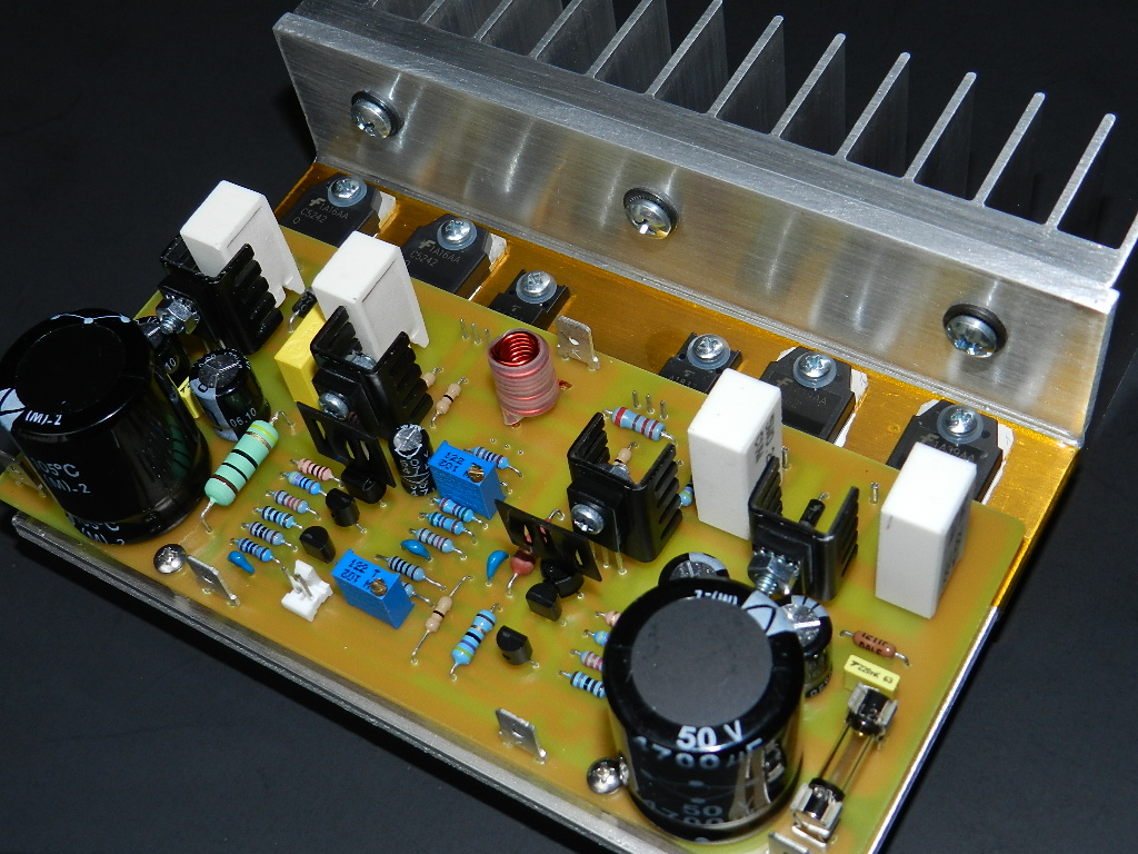
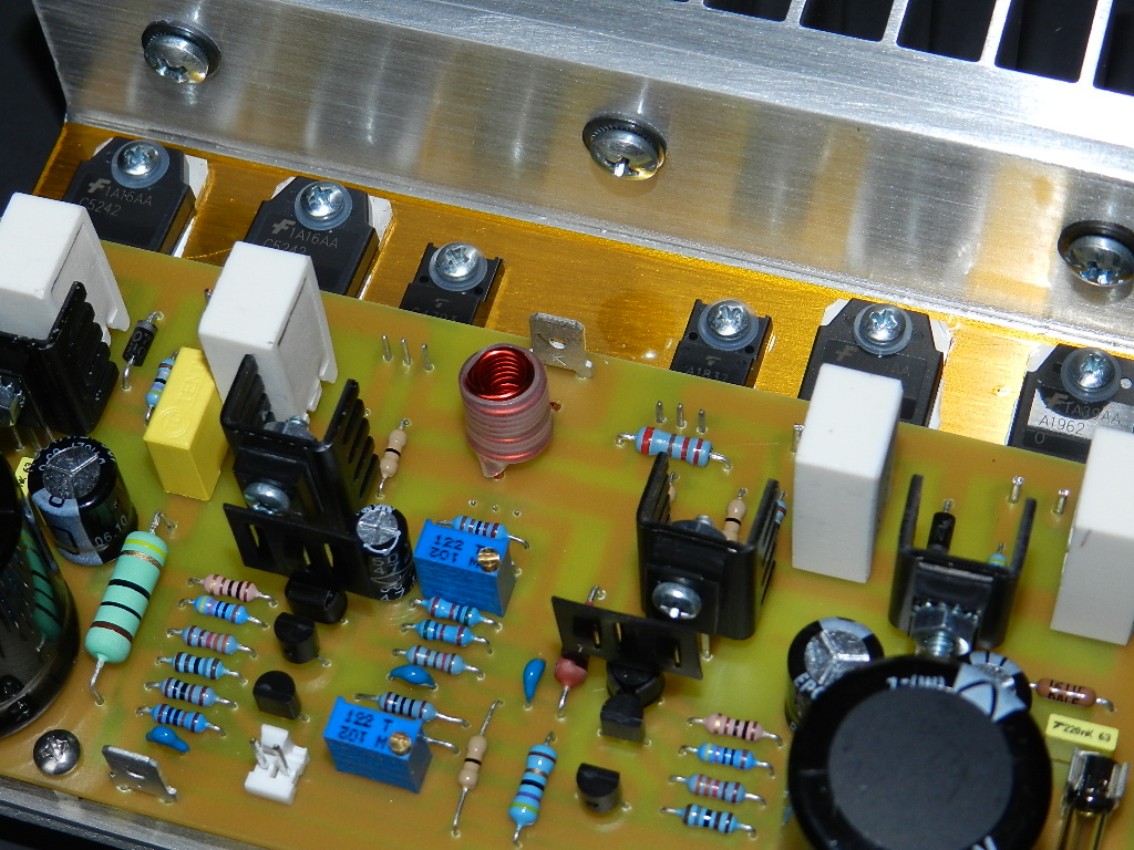
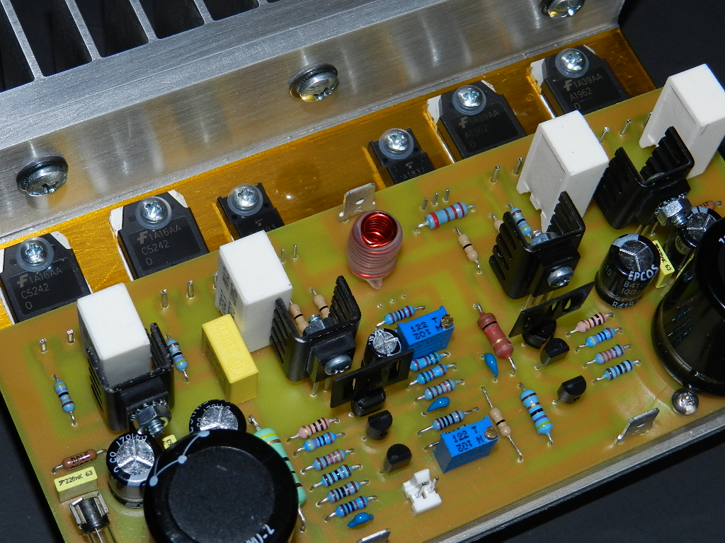
The prototype was built on a 6” X 2.725” single sided PCB. All populated components are standard readily available parts at the time of writing. If you are interested in building this project and have read the Information and Policies section of this website, the schematic diagram, PCB layout (available only by request) and BOM are free, as is, no warranty.
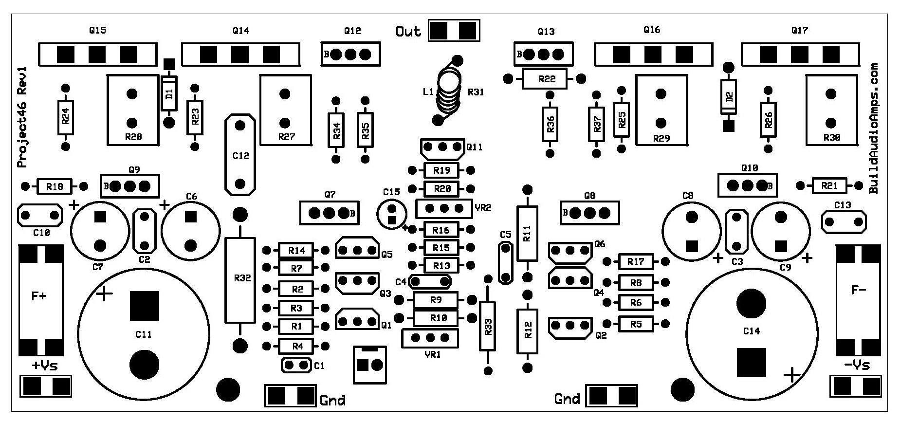 Project 46 Silkscreen and Parts Placement Layer of PCB.
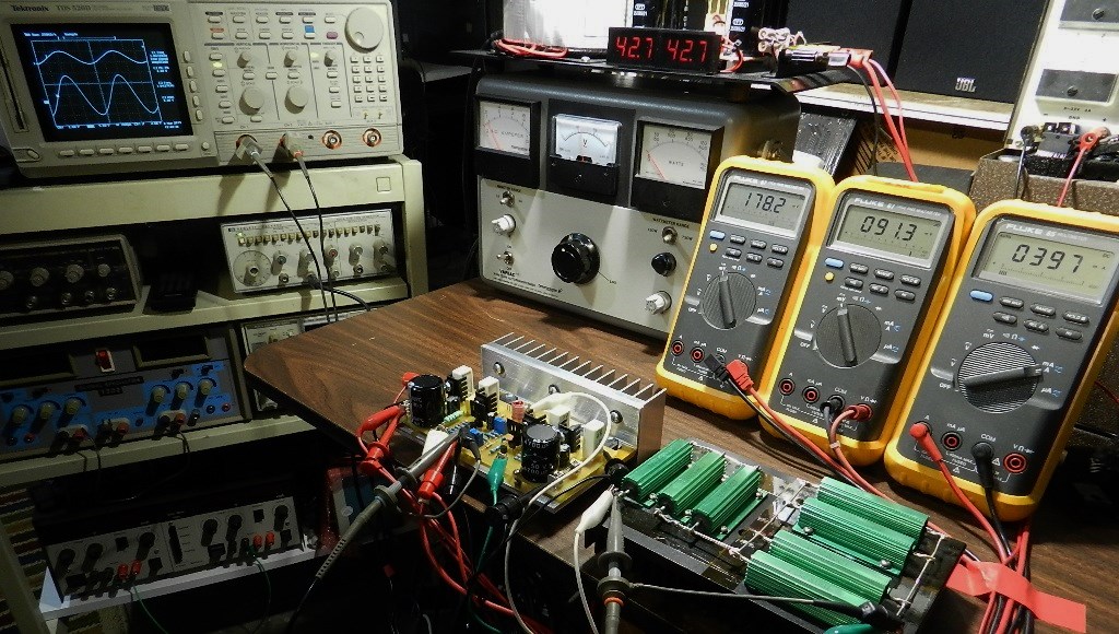
Initial tests. If you have decided to build this project, the idle current needs to be adjusted first before going any further. Insert a jumper or shunt at the input of the amplifier. Do not connect any load or loudspeaker at the output of the amplifier. Adjust VR2 for maximum resistance of 1KΩ; please refer to the schematic diagram where to access VR2 on top of PCB. Leave VR1’s adjustment as is, at this time. Prepare 3 DMMs; to measure the DC offset voltage at the output of the amplifier, the voltage between the emitters of Q15 and Q17, and the overall current across the F+ fuse terminals.
It is highly recommended to use a Variac transformer during the initial test. If something goes wrong with the PCB assembly, minimum damage will occur to the populated components or at least just a blown Variac’s fuse. However both test procedures with or without the use of a Variac transformer will be explained.
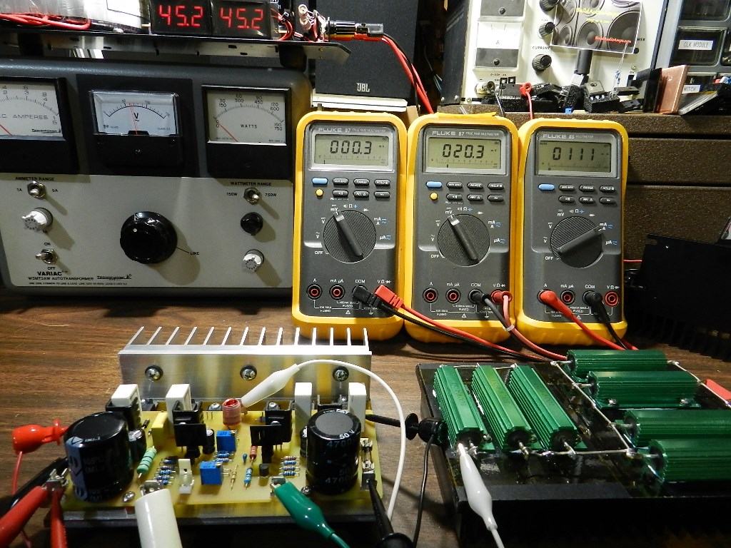
If a Variac transformer is available, connect the AC input of the power supply to the output of the Variac transformer. Switch the power to ON and gradually adjust the Variac’s AC output from zero until the output voltage of the power supply reaches approximately ±35VDC or ±45VDC while observing for sudden increase in any DMM readings. If you have encountered an unusual increase in any of the DMM readings, switch the power to OFF immediately and check the PCB for assembly errors. The picture above shows a DC offset voltage at 0.3mV and could be anywhere within ±20mV. In reality this DMM reading drifts within ±5mV. In my opinion, this is acceptable with no degradation to the audio quality. Adjust VR1 slowly at this time to get as close as possible to 0mV DMM reading and it may need to be readjusted after 10 minutes or more. The voltage between the emitters of Q15 and Q17 is about 20.3mV; readjust VR2 to get approximately to this DMM reading after a warm-up period of about 10 minutes or more. The current across the F+ fuse terminals is about 111mA; this value is dependent on the adjustment of VR2. If you obtain similar DMM readings, you may proceed with music test.
If a Variac transformer is unavailable, make sure that the power supply was properly built and that the output voltage rails have been measured at approximately ±35VDC or ±45VDC before connecting it to the amplifier under test. With the power supply switched to OFF, adjust VR2 for maximum resistance. Leave VR1’s adjustment at this time. Switch the power supply to ON; the DMM measuring the voltage between the emitters of power transistors, Q15 and Q17, should read less than 1mV. The DMM measuring the offset voltage should read anywhere from ±100mV or more. The DMM across the fuse terminals should read about 30mA or less. Other than those DMM readings mentioned, power OFF immediately and check the PCB for assembly errors. When the error was corrected, adjust VR2 to get a DMM reading of about 20mV after a warm-up period of 10 minutes or more. Adjust VR1 slowly to read as close as possible at 0mV DMM reading, this may need to be readjusted after the warm up period. The DMM that’s connected across the F+ fuse terminals will read approximately 111mA of total current, which is dependent on VR2’s setting. If you obtain similar DMM readings, you may proceed with music test.
Optional tests. The next test procedure is optional, but if an oscilloscope, audio signal generator and 8Ω dummy load are available, the maximum power output before clipping can be measured. Be careful not to touch the project’s heatsink and dummy load, it will get very hot during this test.
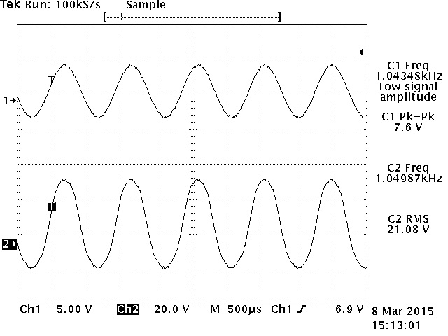
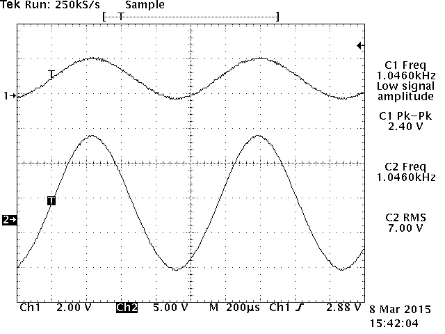
The power output was measured using an HP3312A Function Generator set at 7.6Vp-p sine wave and connected directly to the input of the amplifier, as well as the CH1 test probe of the oscilloscope. An 8Ω dummy load was connected at the output of the amplifier under test as well as the CH2 test probe of the Tektronix TDS520D 500MHz DPO. The prototype produces 21.08Vrms before clipping across the 8Ω dummy load or a power output of more than 55watts at 8Ω or 110watts at 4Ω, as shown in the TEK hardcopy pictures above. The next Tek hardcopy pictures will show a closer look at the waveforms when the input signal was attenuated at 2.0Vpp and 2.4Vpp respectively. The horizontal scale of the oscilloscope was set at 200uS to visually check for artefacts or any other distortions that maybe present.

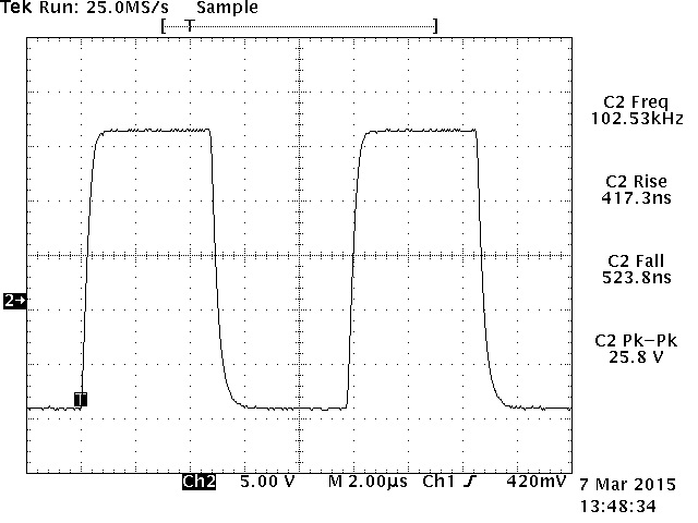
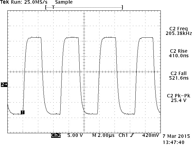
The slew rate was measured using an HP3312A Function Generator set for square wave output, initially at 100KHz then increased to 200KHz at about 25Vpp. The Zobel network at the output of the amplifier was disconnected during this test, to avoid zapping the 10Ω 3watt resistor when a continuous high frequency square wave signal is applied to the input of the amplifier under test. The function generator’s output is connected directly to the input of the amplifier, as well as the CH1 test probe of the oscilloscope. The CH2 test probe of the Tektronix TDS520D 500MHz DPO was connected at the output of the amplifier under test with the dummy load removed. The project’s prototype produces for the 102KHz, a rise time at 417.3nS. While at 205KHz, the rise time is 410nS, as shown in the TEK hardcopy pictures below. These rise times correspond to a slew rate of 188V/uS and 192V/uS respectively.
“One of the worst-kept secrets in audio engineering is that what we hear does not always correlate with what we measure” – Richard C. Heyser
After tinkering with the required initial tests, next is what’s considered to be the best part of building this project, the listening test. The prototype unit was connected to a modified LM49720 tone control preamp. While playing a live recording of “The Train Song“ from Holly Cole’s “The Best of Holly Cole” album on a Toshiba HD-A2 player and Kenwood MV-9D monitor speaker, impressive clarity and dynamics on the entire audio frequency spectrum were experienced. Worth mentioning are tracks 5, 7 and 8 on the same album. The entirety of Sofa Surfers’ “Transit” album, was also auditioned with the same setup for endurance music testing.