Project 36
Project 36 is the simplest symmetrical input stage topology that can be built with relatively few components. The entire audio power amplifier is completely symmetrical and it works. The complementary differential input amplifiers contribute remarkably in reducing distortions. These differential amplifiers are loaded by constant current sources that are symmetrical as well. The voltage amplifier stage of this project is arranged in a push-pull common-emitter configuration. The power output stage consists of common-source configured MOSFET devices.
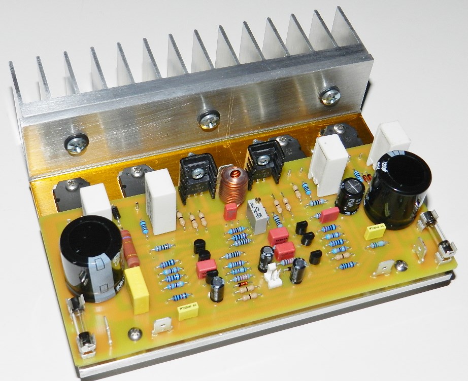
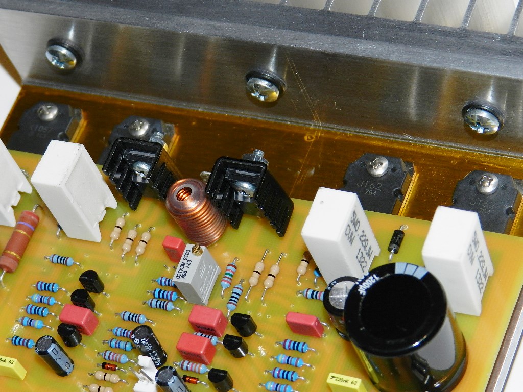
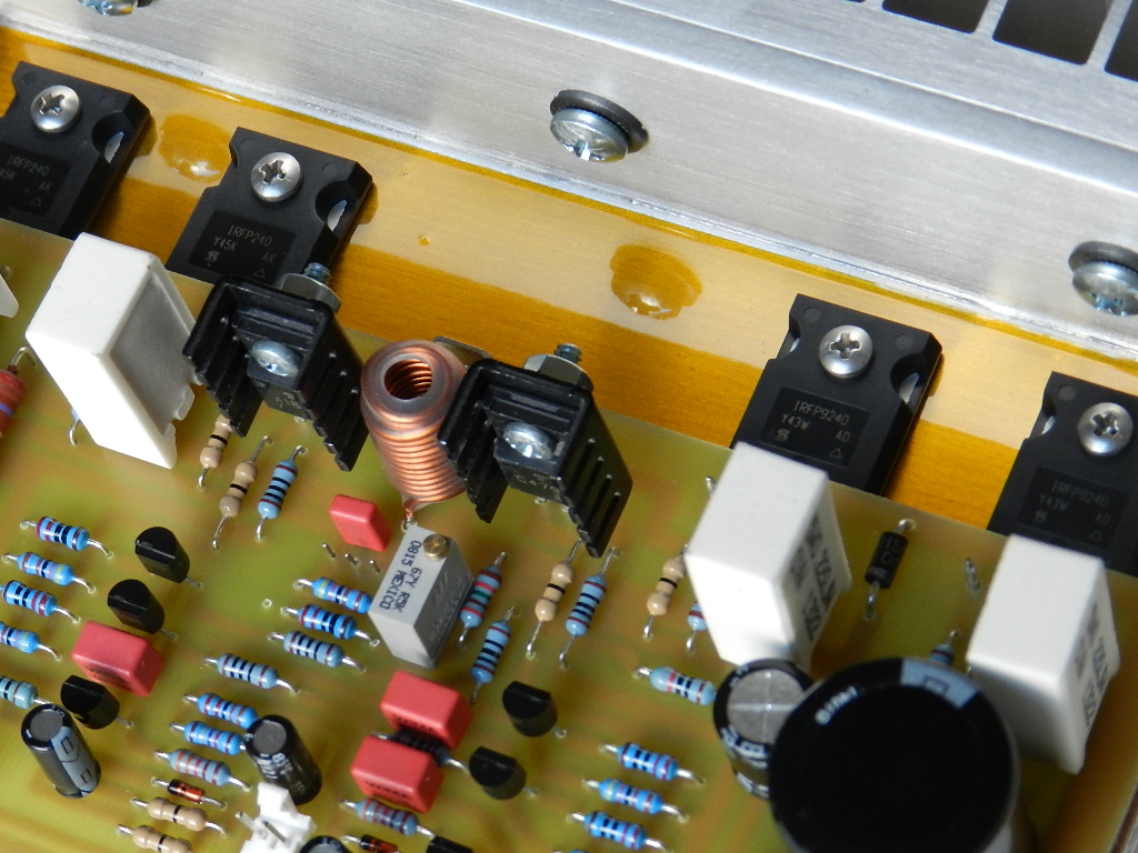
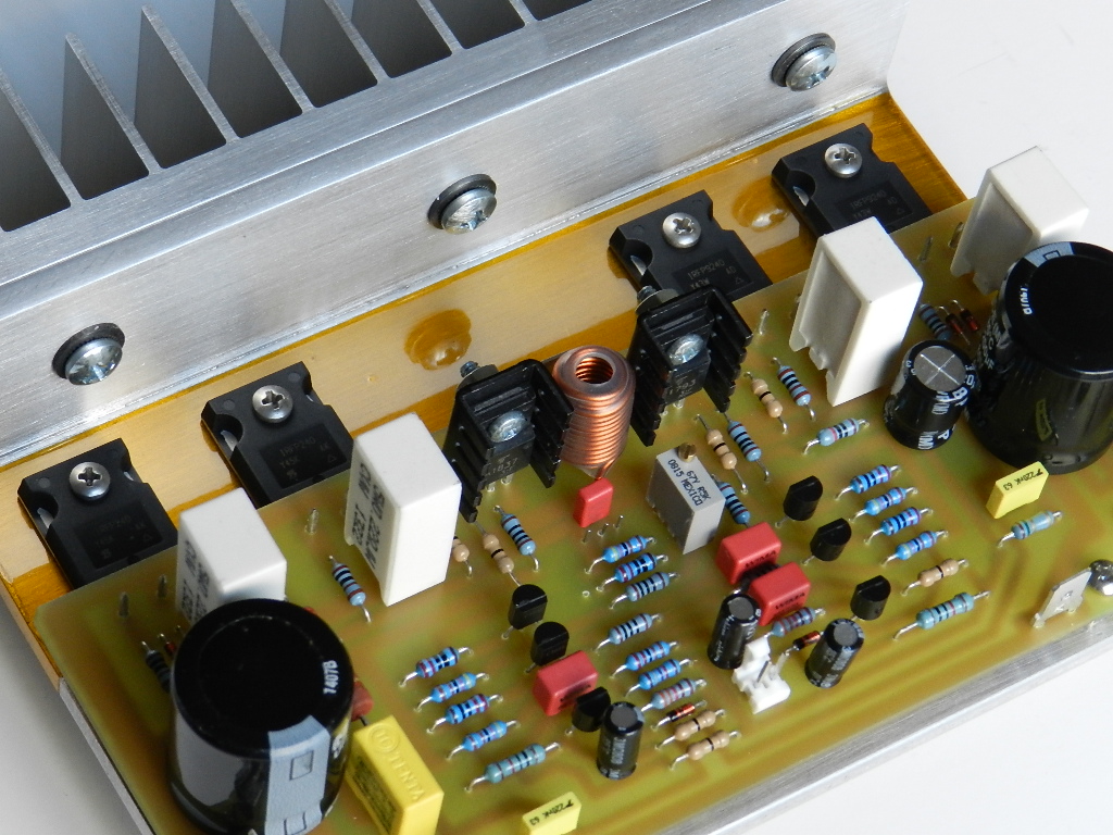
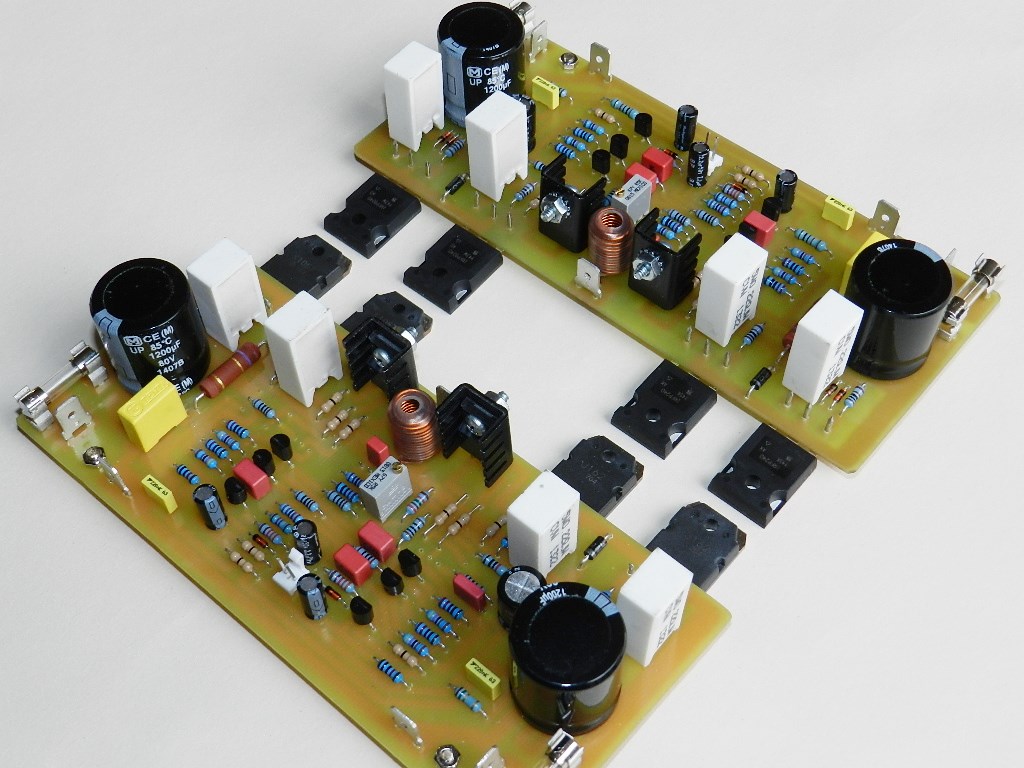
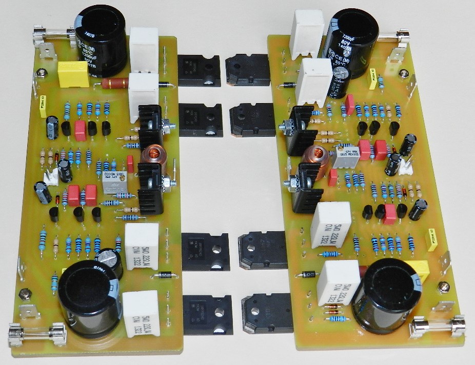
There are two versions of Project 36’s power output stage, as shown in the header pictures above. Version One uses lateral power MOSFETs, the last remaining 2SK1057/58 and 2SJ161/62 in The Parts Bin while Version Two uses HEXFETs, the IRFP240 and IRFP9240. Both versions produces more than 100 watts of audio power at 8Ω load with ±49VDC to ±55VDC power supply rails. Both versions have identical input and voltage amplifier stages. One important thing to note is the package pin-outs for both MOSFET devices are different, so keep that in mind when creating your own PCBs.
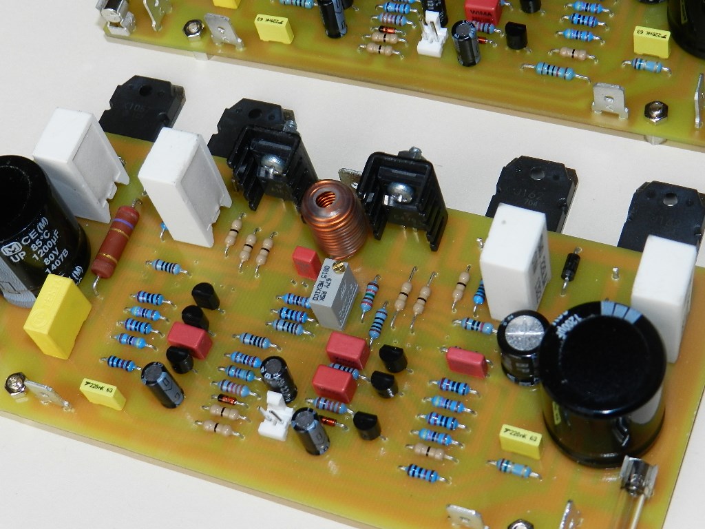
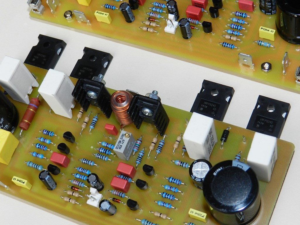
Please refer to the schematic diagram from here on. The front-end of the project consists of two differential amplifiers, Q1, Q2 and Q5, Q6 loaded by two current sources, Q3, D1 and Q4, D2. The current sources are adjusted to about 2mA and determined by the value of R8 and R9. The output of Q1 and Q5 are connected to the common-emitter configured voltage amplifier transistors, Q7 and Q8, high frequency compensated by C14 and C15. The outputs of the voltage amplifier stages are connected to the gates of the power output transistors, Q10 through Q13, by way of gate resistors, R28 through R31. The bias of the power output transistors is set by VR1 and Q9 at approximately 55mA. D3 through D6 are protection diodes against high voltage spikes from reaching the gates of the power output transistors. The gain of the amplifier is set by the value of R21 and R27 at about 27dB. An interesting feature of this project is the addition of CF1 in parallel with R27 and CF2 in parallel with R21. Both capacitors audibly improve the overall frequency response of the amplifier, as mentioned earlier in Project 34.
During music test, when matched with a modified LME49720 tone control preamp, a Toshiba HD-A2 player and several speakers, this project performed very well. But when mated with the LM1036 tone control Project 9, the LM1036 just can’t keep up with recording transients in some tracks of Maroon5’s Songs About Jane album. That’s when the vocals or the band reaches a crescendo; there is a raspy or distorted quality to the sound. However, when PreAmp1 was mated with this project, the listening experience was vastly improved, removing the distortions and improving the fidelity of audio reproduction. PreAmp1 project perfectly matched with this project, but please note that some passive modifications were made at R1’s location of PreAmp1.
If you are interested in building this project and have read the Information and Policies section of this website, the schematic diagram, PCB layout (available only by request) and BOM are free, as is, no warranty.
 Project 36 Silkscreen Parts Placement Layer of PCB.
If you’ve decided to build this project, the idle current needs to be adjusted first before going any further. Insert a jumper or shunt at the input of the amplifier. Do not connect any load or loudspeaker at the output of the amplifier. Adjust VR1 for maximum resistance of 5KΩ; please refer to the schematic diagram where to access VR1 on top of PCB. Prepare 3 DMMs (experienced amp builders have more than 3 DMMs) to measure the DC offset voltage at the output of the amplifier, the voltage drop of the source resistor in any of the power MOSFETs, Q10 through Q13 and the overall current across the F+ fuse terminals. The next pictures will show the lateral and vertical MOSFETs’ almost identical test results.
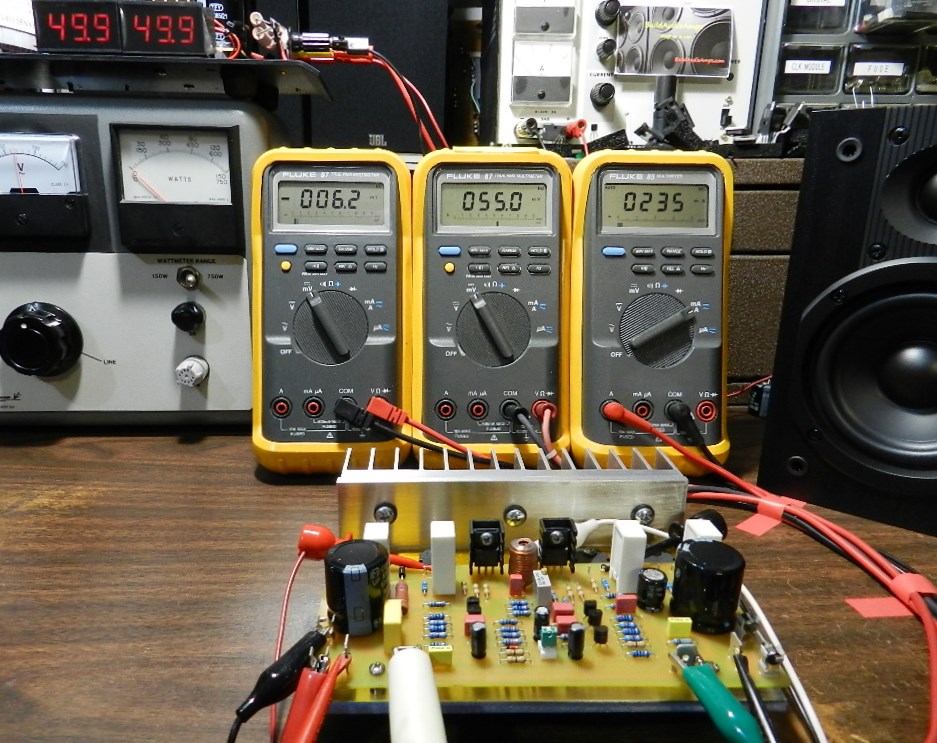
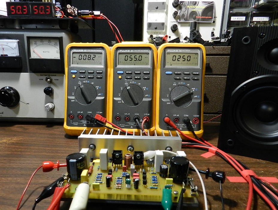
Lateral MOSFETs’ test setup result. Vertical MOSFETs’ test setup result.
If a Variac transformer is available, connect the AC input of the power supply to the output of the Variac transformer. Switch the power to ON and gradually adjust the Variac’s AC output from zero until the voltage output of the power supply reaches approximately ±49VDC to ±55VDC while keeping an eye on sudden increase in any DMM readings. If you have encountered an unusual increase in any of the DMM readings, switch the power to OFF immediately and check the PCB for assembly errors. The picture above shows a DC offset voltage at 6.2mV / 8.2mV and this could be within +/-10mV. The voltage drop across any source resistor is about 55mV; readjust VR1 to get a DMM reading from 20mV to 55mV after 10 minutes of warm-up time. The current across the F+ fuse terminals is 235mA / 250mA; this value is dependent on the adjustment of VR1 and could be from 120mA to 260mA. If you obtain similar DMM readings, you may proceed with music test. One thing you will notice in the music test is that there is no power ON thump and the amplifier is very quiet during the pause between tracks, of course, it’s dependent on how noisy your pre-amp is.
If a Variac transformer is unavailable, make sure that the power supply was properly built and that the output voltage rails have been measured at approximately ±49VDC to ±55VDC before connecting it to the amplifier project under test. With the power supply switched to OFF, adjust VR1 for maximum resistance. Switch the power supply to ON; the DMM measuring the voltage drop across any source resistor should read less than 55mV. If the DMM reading is more than 55mV and cannot be adjusted by VR1, power OFF immediately and check the PCB for assembly errors. If the DMM reading is less than 55mV, adjust the reading from 20mV to about 55mV after 10 minutes. The DMM that is connected across the F+ fuse terminals will read about 130mA to 260mA of total current. If you obtain similar DMM readings, you may proceed with music test.
The next test procedure is optional, but if an oscilloscope, audio signal generator and 8-ohm dummy load are available, the maximum power output before clipping can be measured. Be careful not to touch the project’s heatsink, it will get very hot during this test!

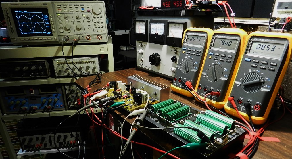
Lateral MOSFETs’ power measurement setup. Vertical MOSFETs’ power measurement setup.
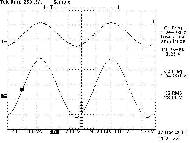
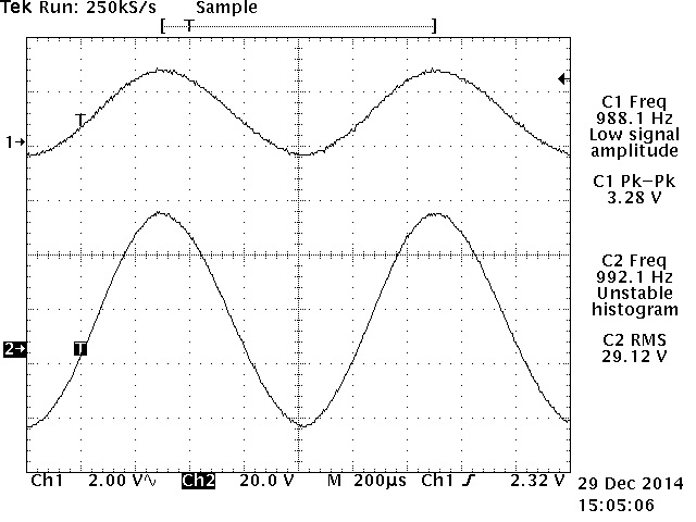
Lateral MOSFETs’ Tek hardcopy test result. Vertical MOSFETs’ Tek hardcopy test result.
The power output was measured using an HP3312A Function Generator set at 1KHz 3.28Vp-p sine wave output and connected directly to the input of the amplifier under test as well as the CH1 test probe of the oscilloscope. An 8Ω/700Watt dummy load was connected at the output of the amplifier under test as well as the CH2 test probe of the Tektronix TDS520D 500MHz DPO. The power amplifier produces a very nice sine wave of 28.66Vrms / 29.12Vrms across the 8Ω/700W dummy load or a power output of more than 100 Watts, as shown in the TEK hardcopy pictures above. The oscilloscope’s horizontal scale was adjusted at 200uS to verify for any visible clipping or artifacts on either peak. This project was paired with a modified PreAmp1 tone control project; the audio quality reproduced was exceptional. Overall, in my opinion, I would prefer the HEXFETs to the SK/SJs but again this is subjective in nature.
For more information on HEXFETs, here’s International Rectifier’s Application Note AN-948, it’s a design of a Linear Power Amplifier using complementary HEXFET Power MOSFETs.