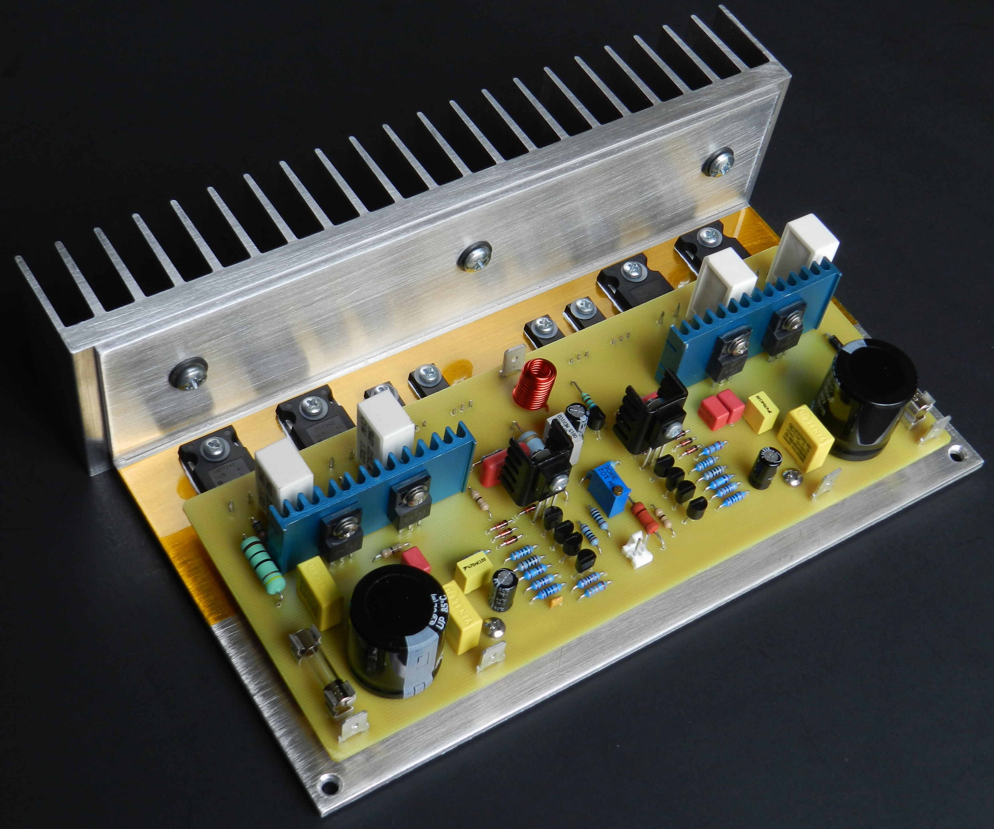
Project 51

Project 51 is another fully symmetrical complementary Current Feedback Amplifier project. The power output stage and temperature sensing network circuit of this project was inspired by the G. Stochino ultra-fast audio power amplifier design from the late ‘90s. However, in this project more power output was realized as compared to the original 100-watt design by changing the drivers, power MOSFETs and power supply rails.
The prototype model was able to achieve 41.1Vrms across an 8Ω dummy load. This corresponds to a power output at approximately 211 watts. The power output before clipping was measured by applying a 1KHz sine wave input signal with an amplitude of 5.8Vpp. The Tek hardcopy picture below on the left shows a very clean amplified replica at CH2 of the input waveform signal at CH1. Also shown below on the right is the actual slew rate measurement at approximately 57V/uS, a far cry from the Stochino’s. Nevertheless, the audio quality as expected is still commendable because of the CFA-based front-end circuit. The slew rate was acquired by applying a continuous 100KHz square wave input signal modestly adjusted to obtain an output amplitude of 22.2Vpp. Although it’s possible to adjust at higher amplitude with no overshoots, it was avoided to prevent repetitive damage and replacement of the power MOSFETs. However, this condition will not occur under normal audio frequency musical input signals.
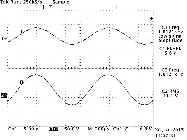
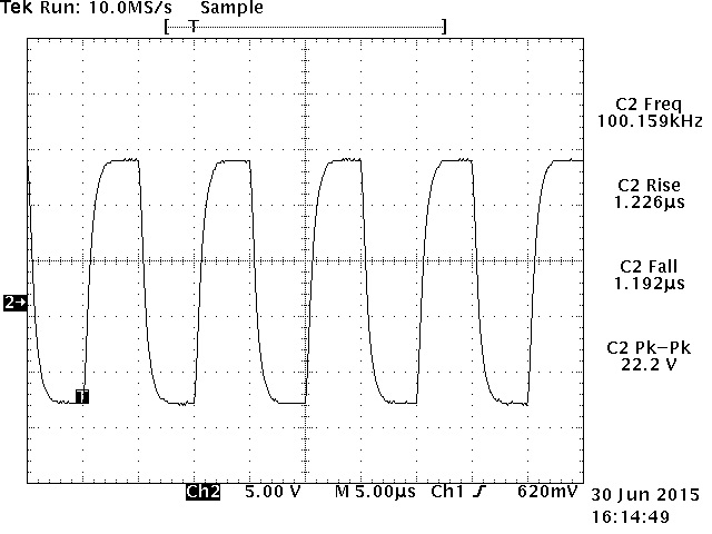
Power output measurement waveform. Slew rate measurement waveform.
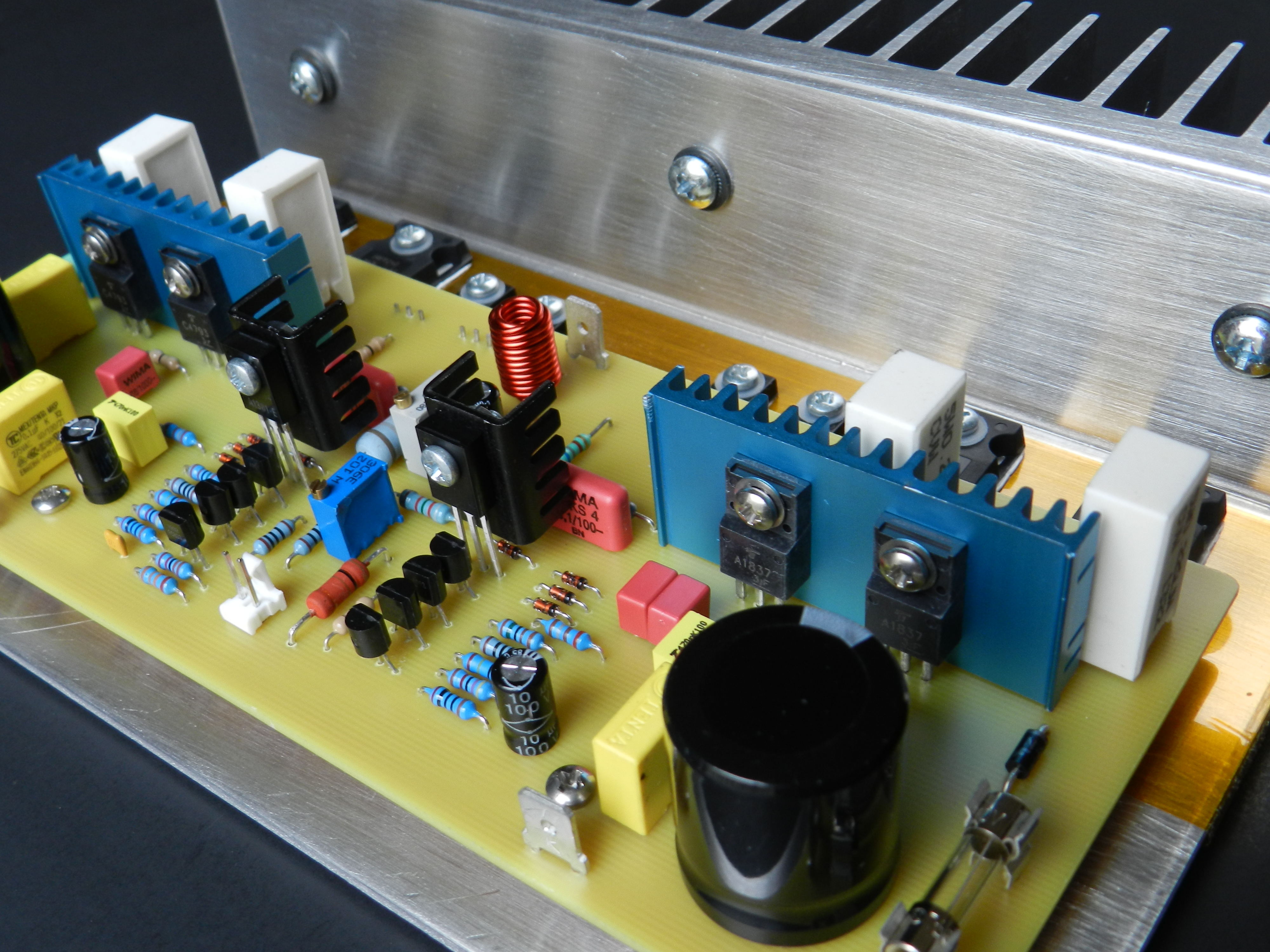
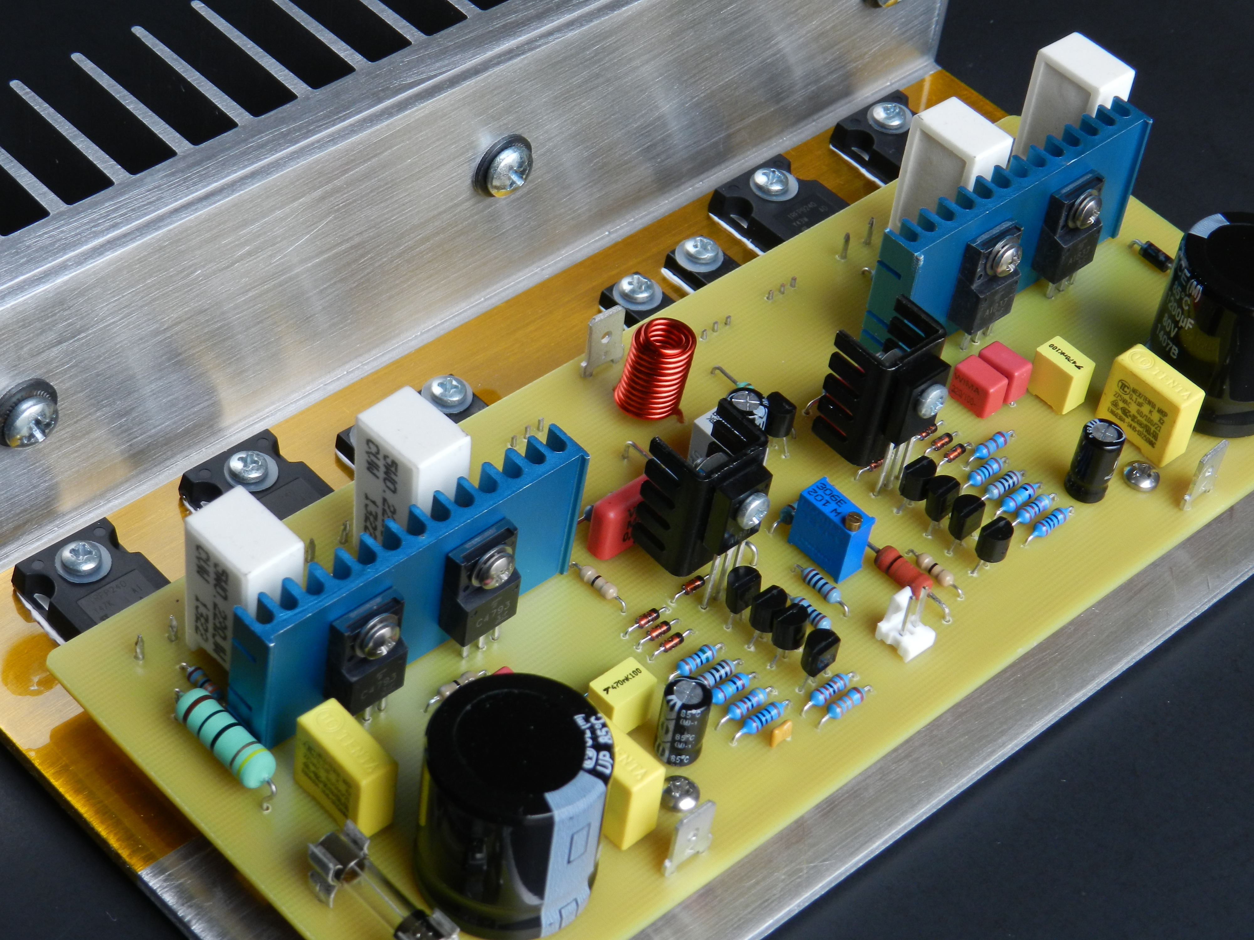
Please refer to the project’s schematic diagram for a brief description of the circuit. The input signal at J1 is directly coupled and passes through a low pass filter consisting of R1 and C1 that suppresses unwanted RF noise from entering the complementary emitter-follower buffer stage transistors, Q1 and Q2. R2 supplies the base bias for Q1 and Q2 and its chosen value also reduces the overall DC offset voltage of the amplifier to minimum. The output of the buffers drives the cascoded summing stage transistors, Q4/Q3 and Q5/Q6. A feedback node consisting of R12 and R13 in parallel with VR1 sets the overall DC offset voltage of the amplifier by ±100mV. If optimum DC offset voltage is desired, an integrator op-amp similar to the one used in Project 4 maybe implemented. However, there’s an improvement to the DC offset settling time in this project compared to previous CFA-based projects because of the additional cascode transistors to the error amplifier stage transistors. Negative feedback resistors, R15 and R31, are also connected in that same feedback node. These resistors determine the overall gain of the amplifier at about 26dB. Changing their values will also change the overall gain of the amplifier.
The outputs of Q3 and Q6 are connected to another cascode arrangement of Q7/Q8 and Q11/Q10. These allow better isolation of the outputs of the input stages from the pre-driver stages. A three-terminal programmable shunt regulator, transistor temperature sensors and VR2, allows the adjustment of the bias setting for the output power MOSFETs.
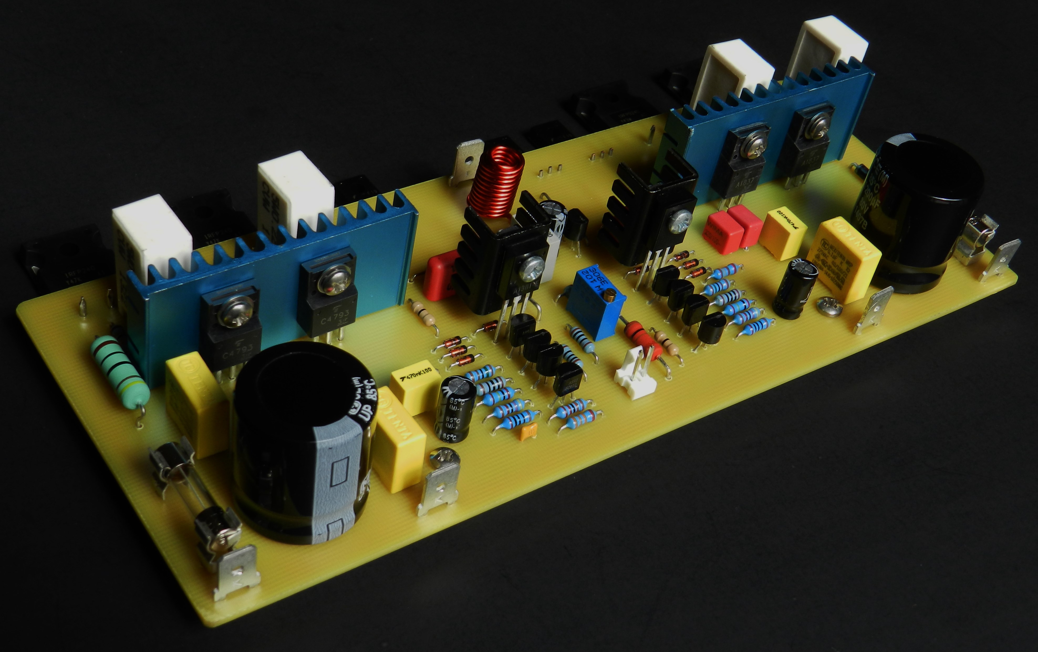
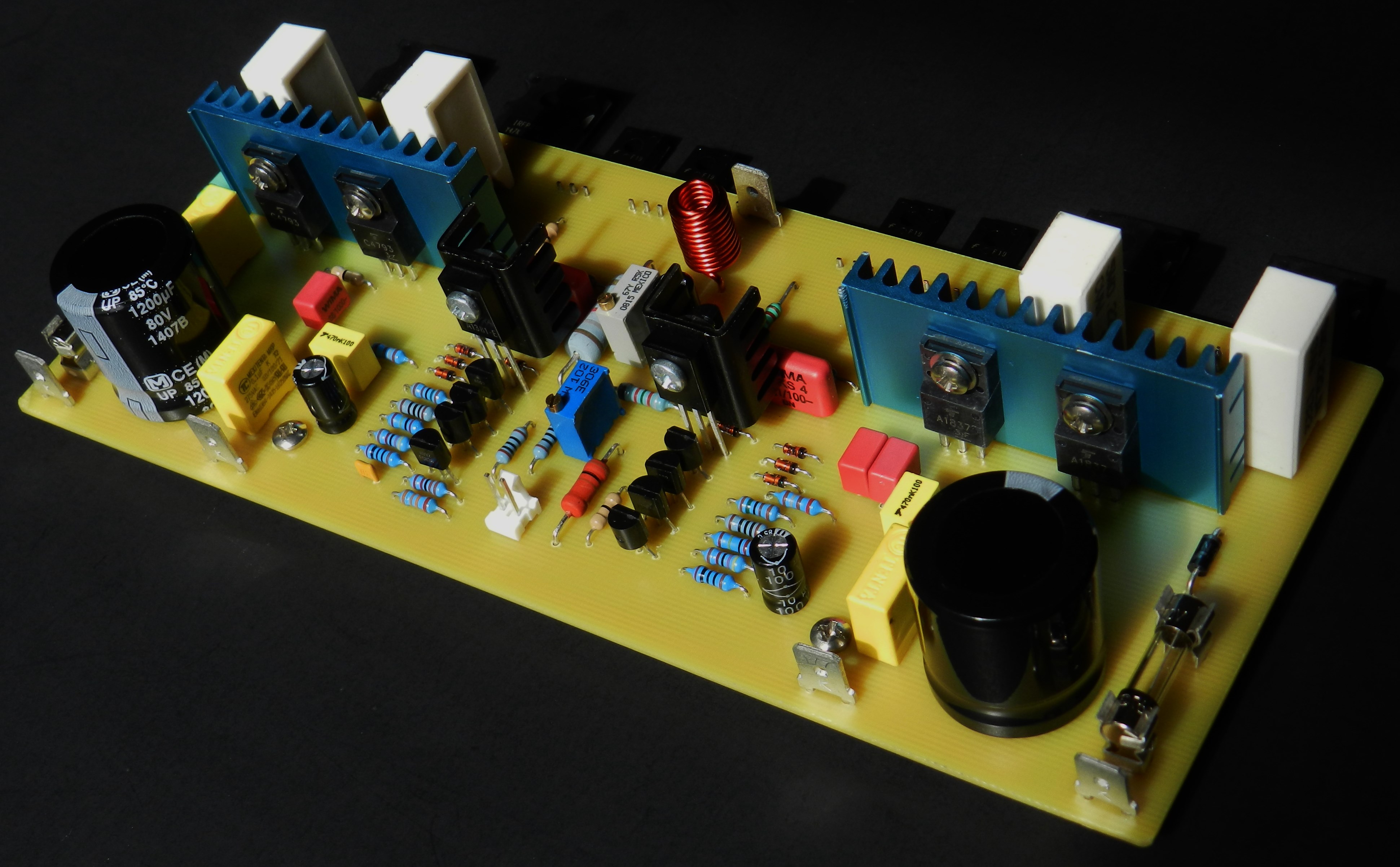
The output stage consists of a complementary pair of T0220-packaged BJT pre-drivers, Q16 through Q19. They isolate the output of Q8 and Q10 from the complementary output power MOSFETs, Q20 through Q23. Additional power output devices may be paralleled to the existing MOSFETs so that it can safely drive very low impedance loads.
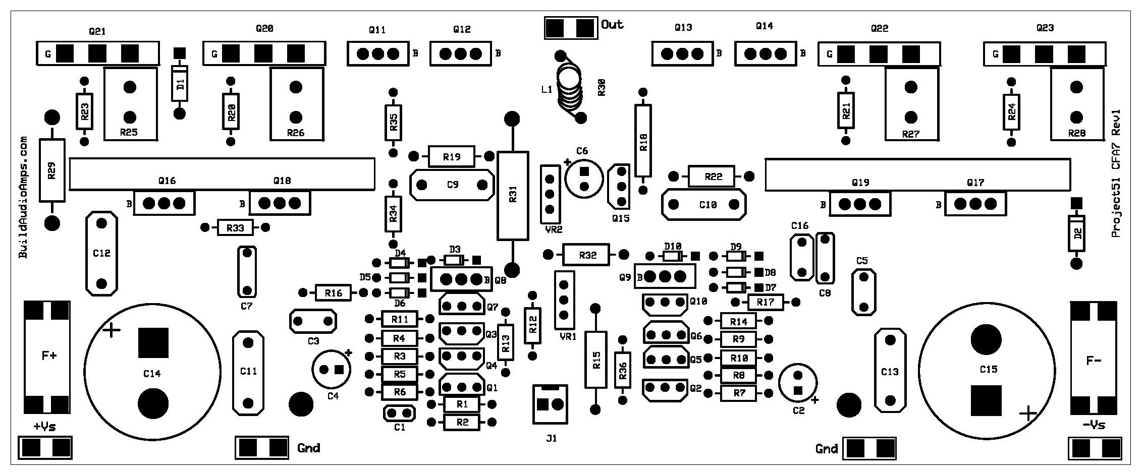
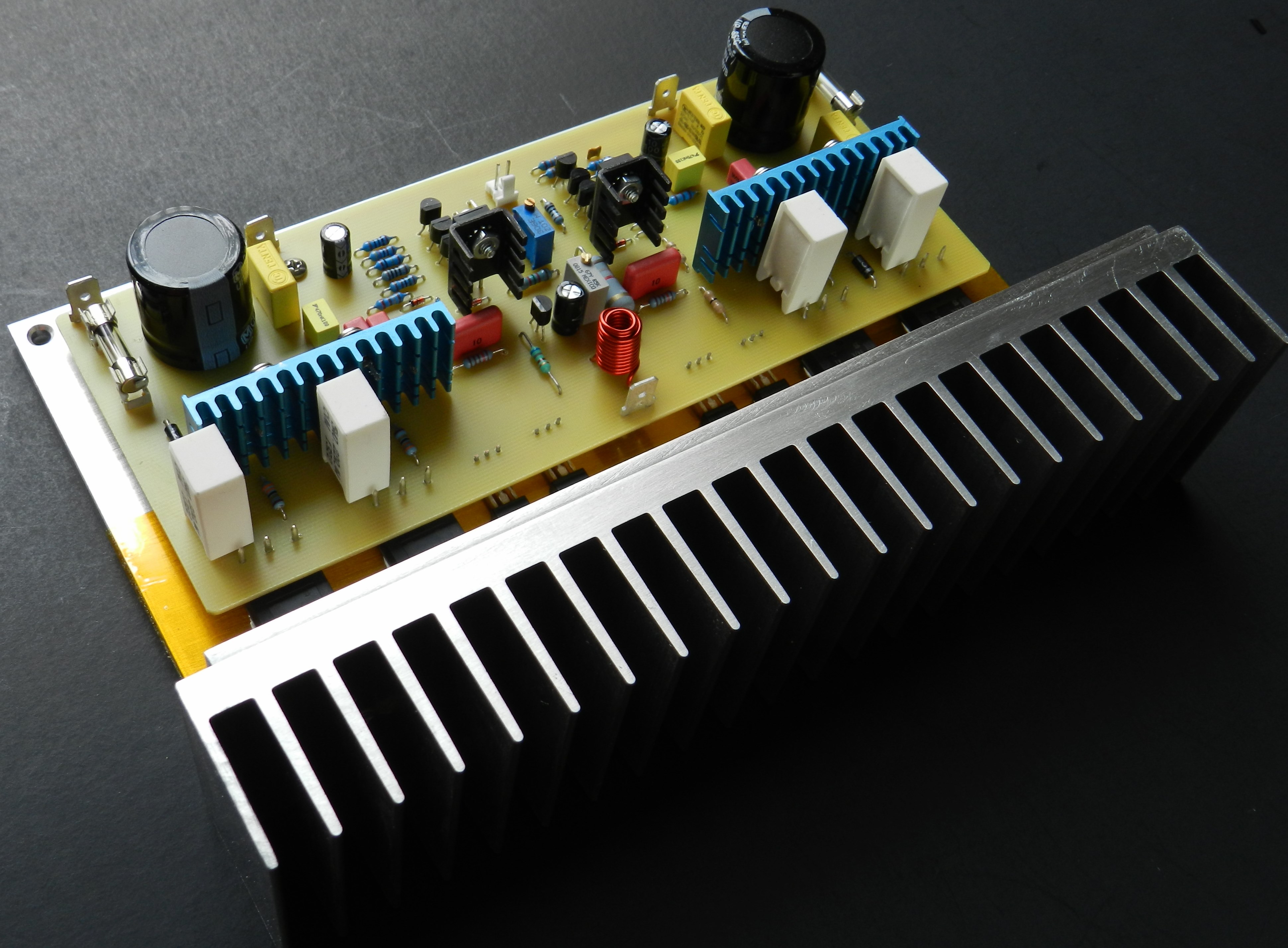
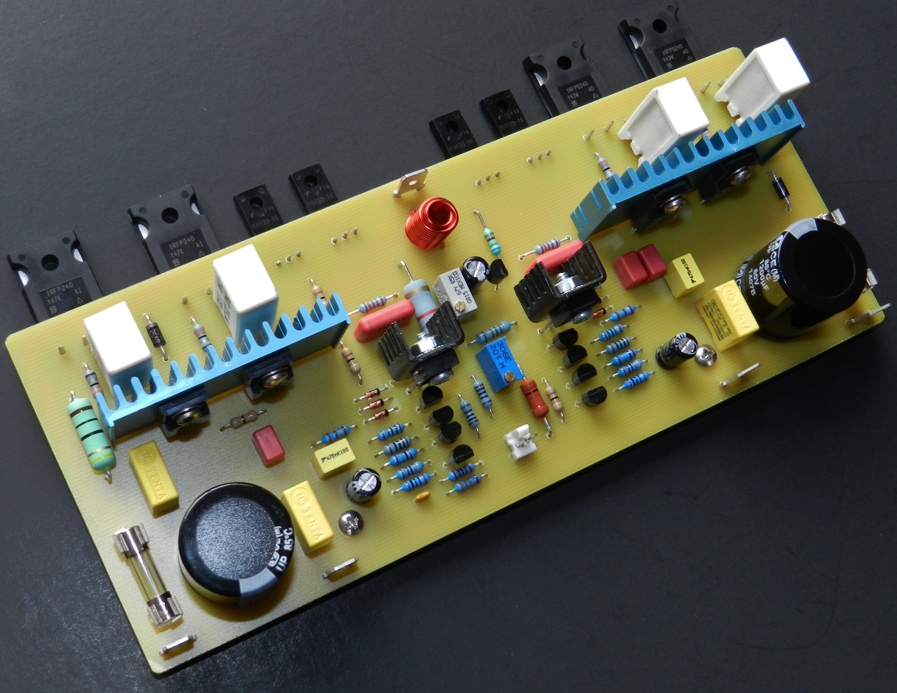
Project 51 Silkscreen and parts placement layer of PCB.
The prototype model was built on a 7.397” X 3.0” single-sided PCB. All components used in the prototype model are readily available standard parts. If you are interested in building this project and have read the Information and Policies section of this website, the schematic diagram, PCB layout (available only by request) and BOM are free, as is, no warranty.
Before powering up the project, be sure to check for very high resistance (∞) ohmmeter reading between drain of all power MOSFETs and the aluminum mounting bracket or heatsink. Also apply a generous amount of heatsink compound to the thermal metal pad of these transistors.
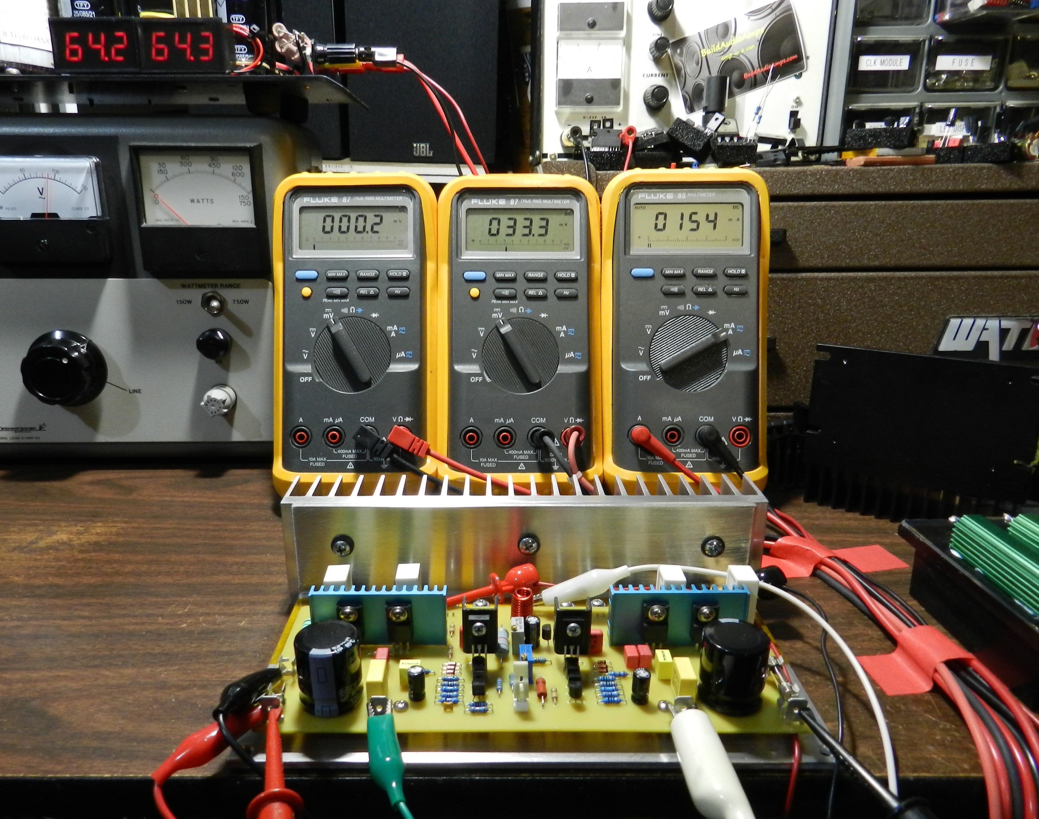
The amplifier requires approximately ±64VDC power supply rails; produced from a rectified and filtered 90VCT at 300VA or higher power transformer. The picture above shows a digital panel voltmeter reading at approximately ±64VDC, obtained by connecting the AC input of the power supply to the AC output of a Variac transformer. Initially adjust the Variac transformer so that the panel voltmeter reads from 0V to about ±64VDC while observing the DMMs: connected at the output of the amplifier, across the source resistors, R26 and R28, and the overall current at F+ fuse terminals. Power off immediately if you have observed higher DMM reading from what’s shown in the picture. Check the PCB for any assembly errors. Apply power to the amplifier again when any fault has been determined and corrected. Allow the amplifier to warm up for more than 15 minutes before making any adjustments.
The DMM on the left side of the picture is measuring the DC offset voltage at 0.2mV, which can be set as close as possible to minimum (0mV) by VR1. The DMM in the middle measures 33.3mV across any source resistors, R25 through R28. This is set by VR2 and it could be anywhere from 20mV to 35mV depending on the builder. The measured voltage between Vref and anode pin of Q15 (near minimum resistance of VR2) is 15mV with a corresponding voltage drop across any power MOSFET source resistors, R25 through R28, at approximately 26mV. Adjusting VR2 at almost maximum resistance (5KΩ) will result to a 100mV reading across Vref and anode pin of Q15. At this setting a 33mV voltage drop will develop across any power MOSFET source resistors. By Ohm’s Law, a 33mV voltage drop across the 0.22Ω source resistor will set the bias at about 150mA for the output power MOSFETs, which was also verified by the 154mA reading of the DMM that’s connected across the F+ fuse terminals.
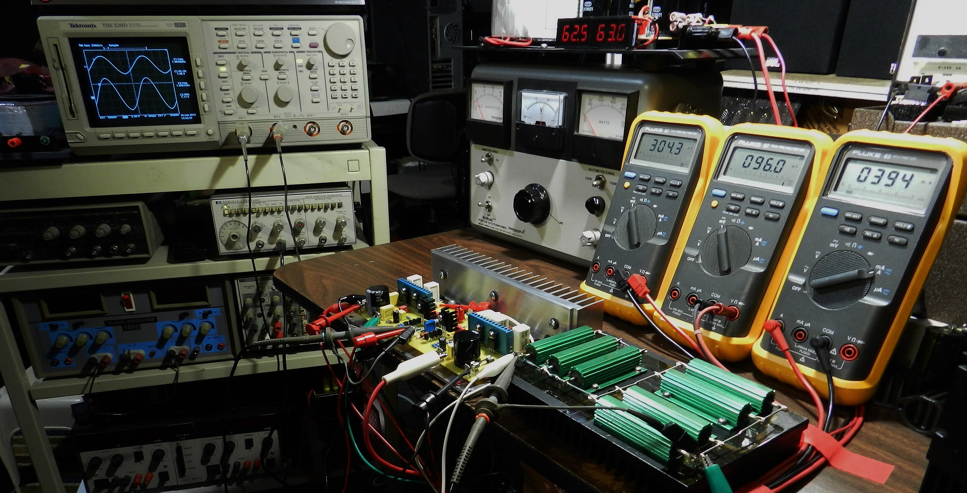
The picture above shows the test setup for power output and slew rate measurements that are optional. An HP3312A function generator and a Tektronix TDS520D 500MHz oscilloscope was used for these particular tests. However, similar equipment may be used if you’re planning to perform the same optional tests. Be careful not to touch the amplifier under test, heatsink and dummy load; they will get very hot!
The dummy load is only connected to the amplifier during power output measurement. It should be disconnected from the output of the amplifier during slew rate measurement. The Zobel network resistor R29, a 10Ω 3W wire wound power resistor, should be disconnected as well. Running a continuous high frequency square wave signal to the amplifier will damage this resistor.
As mentioned and shown earlier, the measured power output of the amplifier before clipping is 211 watts at 8Ω with ±64VDC power supply rails. This power output was achieved by applying a 1KHz at 5.8Vp-p sine wave input signal to the amplifier that resulted to a 41.1Vrms across an 8Ω dummy load. The slew rate was measured by applying a 100KHz square wave signal to the input of the amplifier and its amplitude adjusted to obtain a square wave output waveform at about 22.2Vpp.
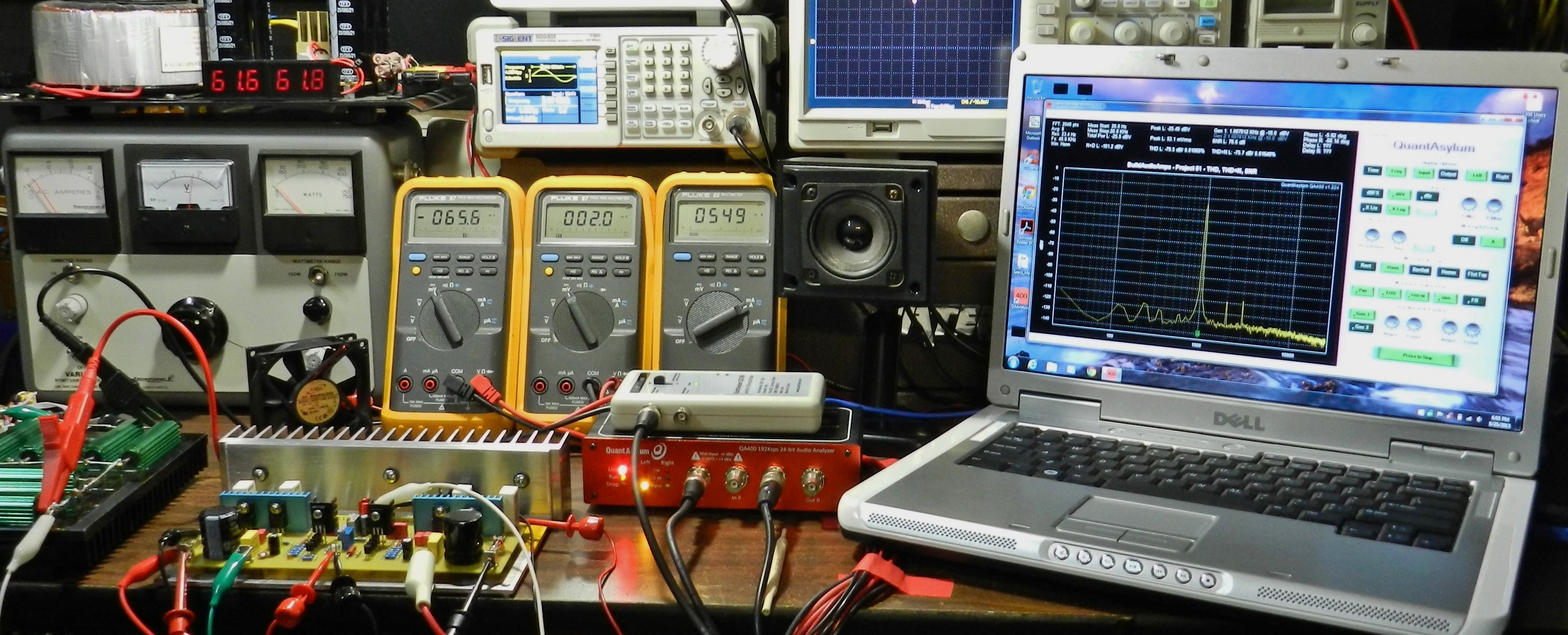
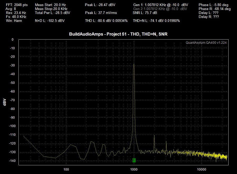
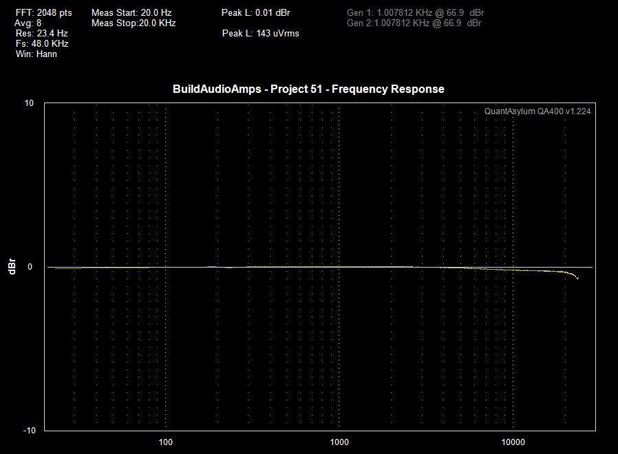
The picture above shows an 8Ω dummy load, Project 51, QA190, QA400, DMMs, Variac/power supply and a Dell laptop computer. This is a simple test setup in performing some basic audio measurements to the power amplifier project with very good results. A QA400 24-bit Real Time Audio Analyzer from QuantAsylum was utilized to measure noise, THD, THD+N, SNR and frequency response. The QA400 is USB powered, controlled by its own application software and can generate and analyze very accurately a series of burst test tones. For this test, the USB hardware was connected to a Dell laptop computer that’s running a Windows 7 operating system.
The input clipping level on the QA400 is +3dBV or 4Vpp. As it is, that’s good enough for testing low voltage level preamplifier or tone control projects. It is however a problem when testing power amplifiers that’s producing very large amount of voltage. To avoid this damaging condition to the QA400, it is necessary to attenuate the high voltage signal coming from the output of the power amplifier project. One of several ways is to connect a QA190 Low Noise Differential Probe to the input of the QA400. The QA190 clamps the high-voltage signal from the output of the amplifier under test to safe level of about ±4 volts. The QA190 is battery powered and is also fitted with a selectable /10 and /100 range switch for convenience. With the protection of the QA190 in place you don’t have to worry about destroying the QA400 and life goes on!
The left or right channel signal generator output of the QA400 is directly connected to the input of the amplifier under test. Depending on the type of measurement, the signal generator generally generates a 1KHz sine wave signal at -10dB with a sweep from 20Hz start frequency up to 20KHz stop frequency span; however, all these values are user definable. You can also safely monitor this signal by connecting an oscilloscope at the input of the amplifier under test. The next captured QA400 display area pictures will show the test results of Project 51.
How does this project sound? The audio quality perceived during music test reveals the wide frequency response of a CFA-based audio power amplifier. In real world listening with various music materials, the experience was excellent. The prototype unit was connected to a modified LM49720 tone control preamp, a Toshiba HD-A2 player and a Kenwood MV-9D monitor speaker. Several CD albums were auditioned during listening test.