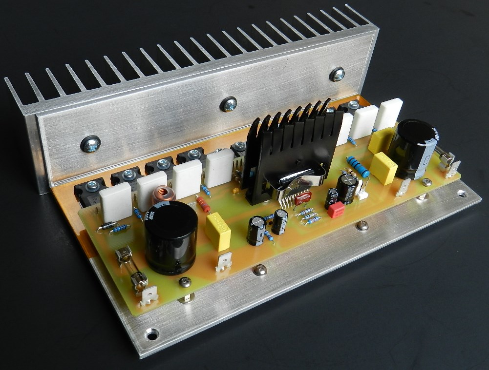
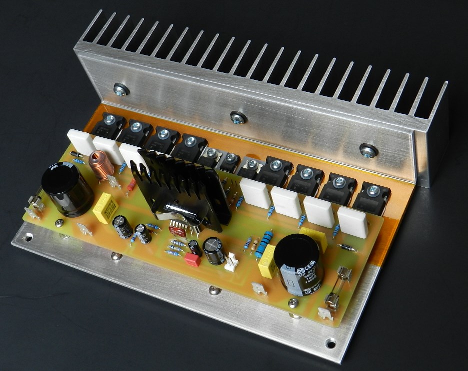
Project 42
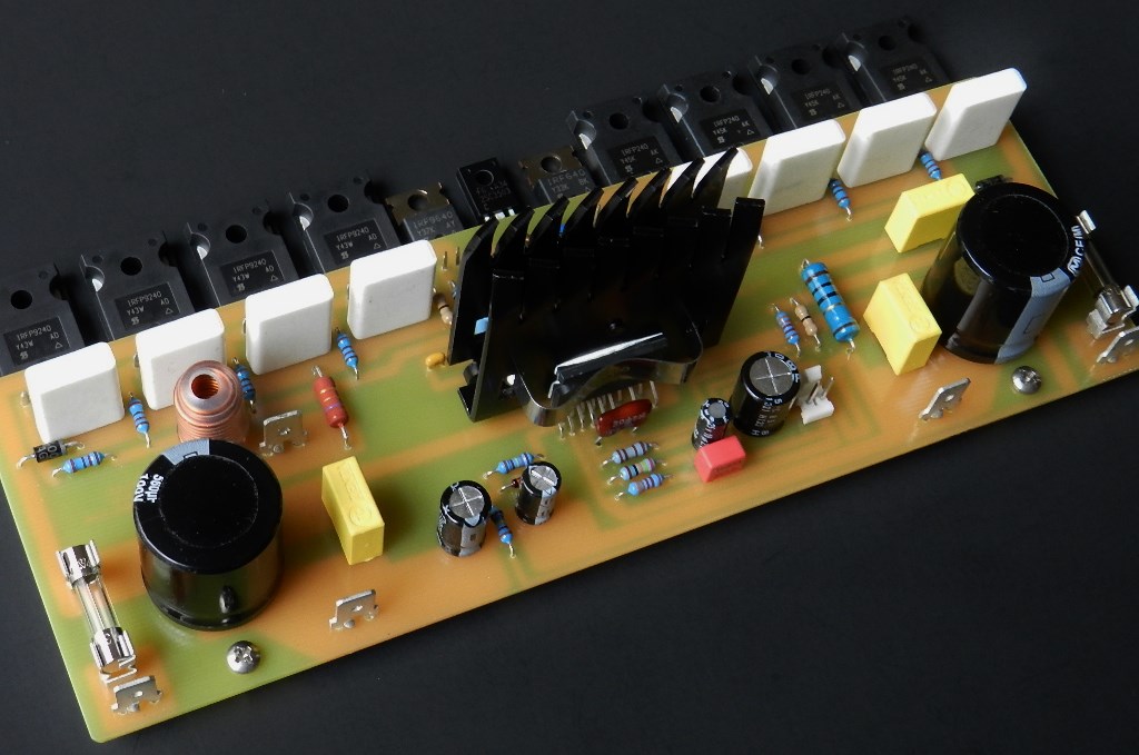
Project 42 is a scaled high-powered version of the previous project on the LME49830 chip. A pair of MOSFET drivers, Q2 and Q7, was added to isolate the LME49830 from the output stage power MOSFETs. The inclusion of these drivers improves the overall frequency response of the amplifier. The measured power output of this project before clipping is about 230 watts at 8Ω load or more than 460 watts at 4Ω load with a ±65VDC to ±75VDC power supply rails.
This project is a non-inverting configuration whose voltage gain is set by R3 and R4 at 29V/V (29.2dB). The wattage value of R31 should be no less than 3W (EP3WS10RJ or similar), because during slew rate measurement, where a 10KHz square wave signal set at 1.2Vp-p was applied to the project’s prototype model, this resistor became too hot and went up in smoke!
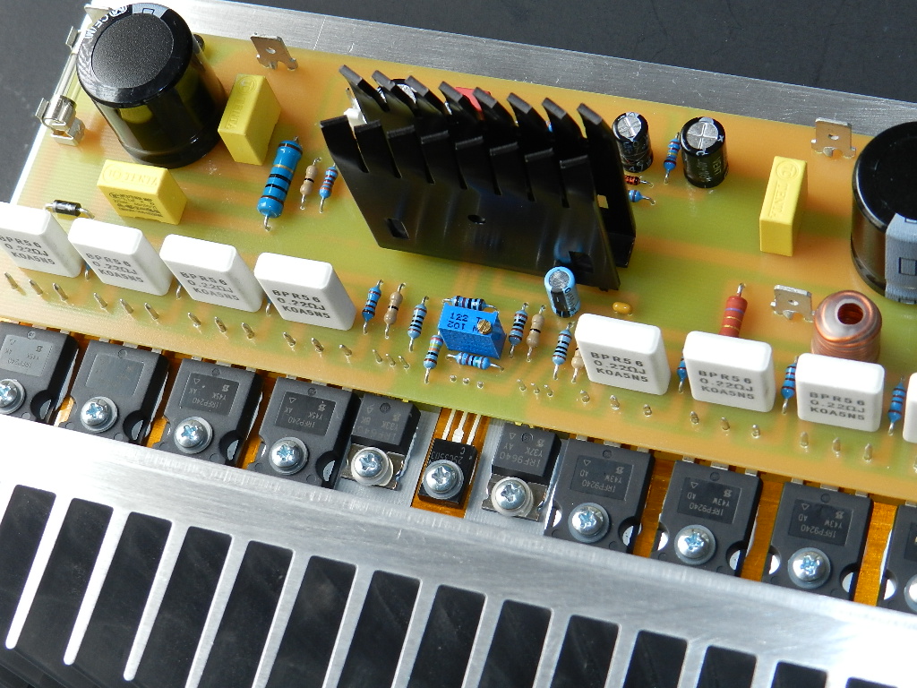
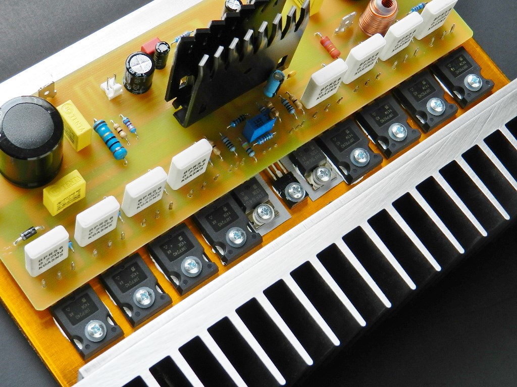
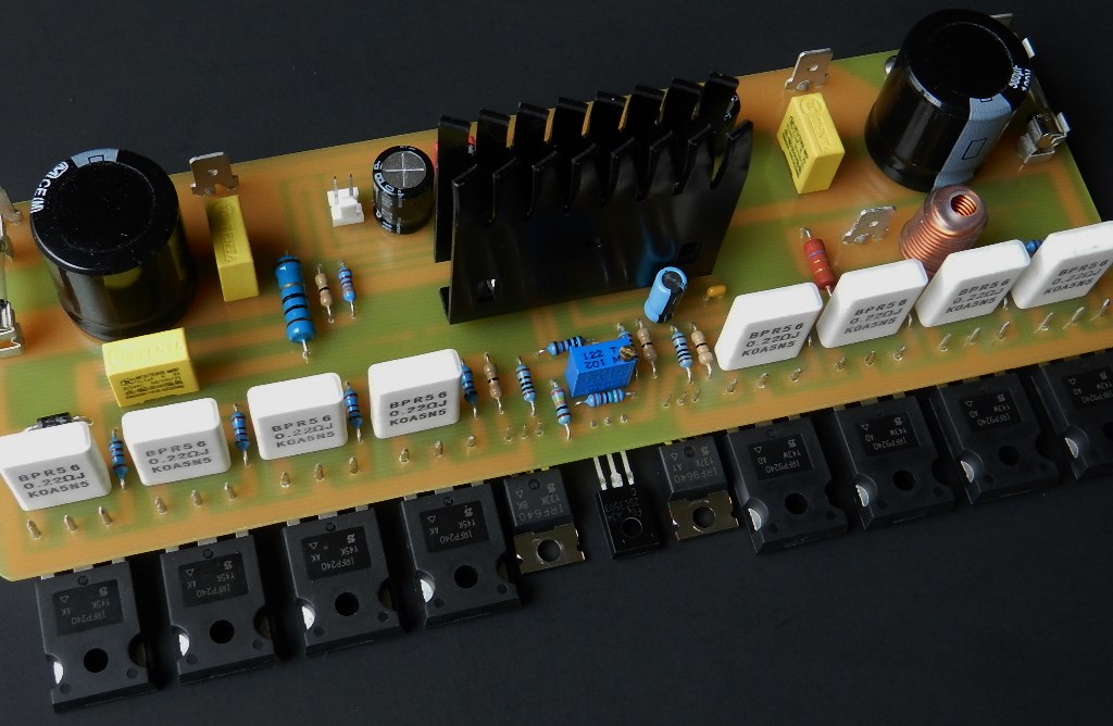
The LME49830 has two external bias control pins at pins 11 for the negative and 12 for the positive. A thermally compensated VBE multiplier circuit consisting of Q1, VR1 and other associated components is connected into these pins to adjust the bias of the power output devices. With this type of circuit arrangement the bias will remain relatively stable over its temperature operating range. The resistance value of R8 was increased as compared to the previous project, to met the demand of higher bias requirement of the paralleled power MOSFETS.
The bias current of about 114mA per transistor was chosen so that crossover distortion is minimized while at the same time keeping low quiescent power dissipation level. In actual power measurement test, VR1 was adjusted so that both peaks of the waveform at maximum power output are well rounded just before clipping occurs and then verifying that same test results with actual sound quality from a listening perspective. The optimized minimum bias setting was determined at about 25mV across any of the source resistors, R22 thru R29. This is time consuming, subjective and you may experience different results but it’s worth tinkering.
After performing the required initial tests, next is what’s considered to be the best part of building this project, the listening test. The prototype unit was connected to a modified LM49720 tone control preamp. While playing “Passion” by Nightmares On Wax from their “N.O.W. Is The Time” album on a Toshiba HD-A2 player and Kenwood’s quad 12” 3-way speakers, impressive clarity and dynamics on the entire audio frequency spectrum was experienced. Listening to one of the finest classic live recording of the Eagles from their “Hell Freezes Over” album reproduced the same musical fidelity experience. The entirety of Portishead’s “Dummy” album was also auditioned with the same setup for endurance music testing.
If you are interested in building this project and have read the Information and Policies section of this website, the schematic diagram, PCB layout (available only by request) and BOM are free, as is, no warranty.
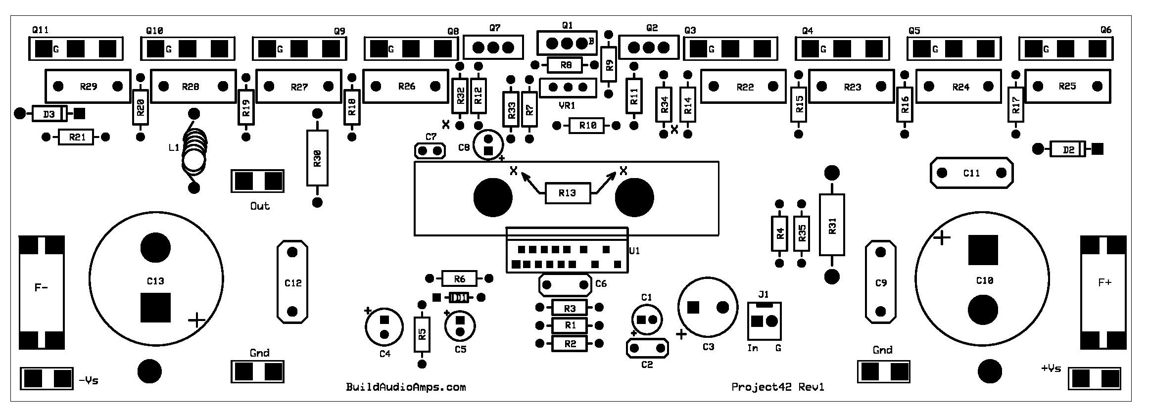
Project 42 Silkscreen Parts Placement Layer of the PCB.
If you’ve then decided to build this project, the idle current needs to be adjusted first before going any further. Insert a jumper or shunt at the input of the amplifier. Do not connect any load or loudspeaker at the output of the amplifier. Adjust VR1 for maximum resistance of 1KΩ; please refer to the schematic diagram where to access VR1 on top of PCB. Prepare 3 DMMs to measure the DC offset voltage at the output of the amplifier, the voltage between the source of Q6 and Q11 and the overall current across the F+ fuse terminals.
Why all the DMMs? The very first time you apply power to a newly built audio amplifier project the DMM is your very best friend. The DMM tells you if there is something wrong with your printed circuit board assembly. A very high ammeter reading indicates that a component in the circuit is drawing too much current. The same goes with a very high voltage reading at the output of the amplifier where you should expect a very low voltage reading in the millivolts range. The DMM tells you the bad news first and when the inevitable happens you immediately switch OFF the power supply and recheck the assembly. If you don't have all the DMMs connected to those important test point locations mentioned and when that tragic event happens, you only have your senses to tell you something is burning or smoke signals are coming off from the populated components. The DMM likewise tells you the good news when everything works just fine and that you did a good job!
It is highly recommended to use a Variac transformer when performing the initial test of the project. If something goes wrong with the project, minimum damage will occur to the components or just a blown Variac’s fuse. However both test procedures with or without the use of a Variac transformer will be explained.
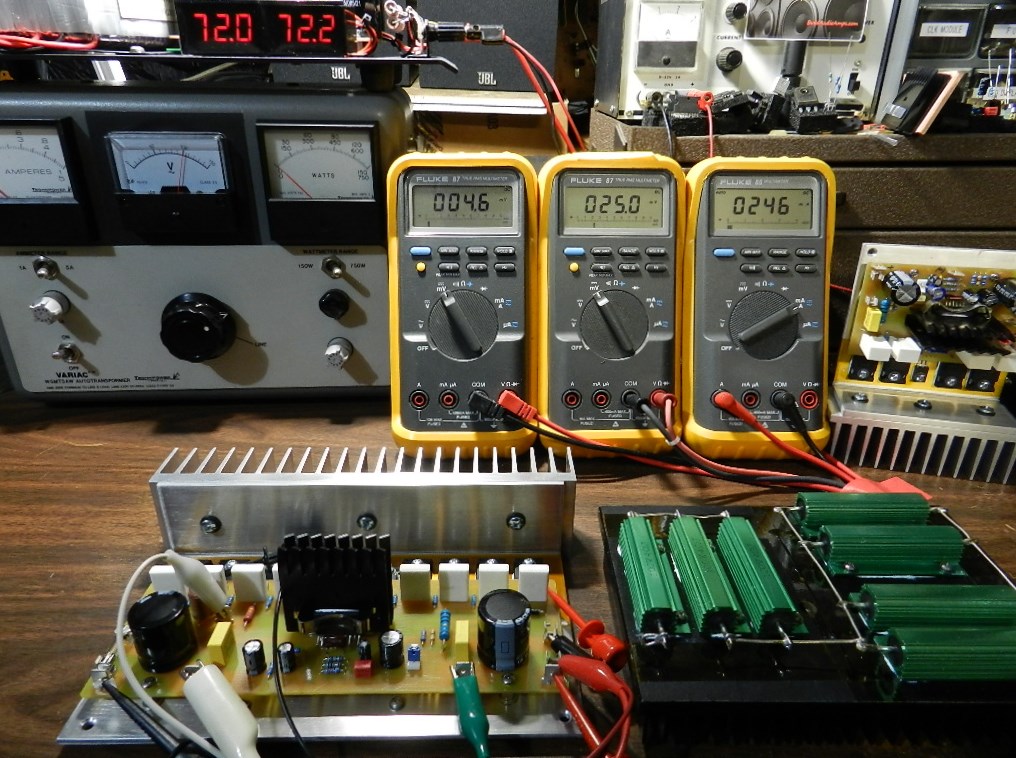
If a Variac transformer is available, connect the AC input of the power supply to the output of the Variac transformer. Switch the power to ON and gradually adjust the Variac’s AC output from zero until the voltage output of the power supply reaches approximately ±72VDC while observing for sudden increase in any DMM readings. If you have encountered an unusual increase in any of the DMM readings, switch the power to OFF immediately and check the PCB for assembly errors. The picture above shows a DC offset voltage at 4.6mV. The voltage between source of Q6 and Q11 is 25mV; readjust VR1 to get approximately that DMM reading after a warm-up period of about 10 minutes or more. From the prototype test results, it was determined that this bias voltage is the minimum actual value that produces a well-rounded peak on the output waveform. The current across the F+ fuse terminals is about 246mA; this value is dependent on the adjustment of VR1. If you obtain similar DMM readings, you may proceed with music test.
If a Variac transformer is unavailable, make sure that the power supply was properly built and that the output voltage rails have been measured approximately ±72VDC before connecting it to the amplifier project under test. With the power supply switched to OFF, adjust VR1 for maximum resistance. Switch the power supply to ON; the DMM measuring the voltage between the source of power transistors, Q6 and Q11, should read less than 1mV. The DMM measuring the offset voltage should read about 4.6mV. The DMM across the fuse terminals should read about 30mA or less. Other than DMM readings mentioned, power OFF immediately and check the PCB for assembly errors. When the error was corrected, adjust VR1 to get a DMM reading of 25mV after a warm-up period of 10 minutes or more. The DMM that’s connected across the F+ fuse terminals will read about 246mA of total current. If you obtain similar DMM readings, you may proceed with music test.
The next test procedure is optional, but if an oscilloscope, audio signal generator and 8Ω dummy load are available, the maximum power output before clipping can be measured. Be careful not to touch the project’s heatsink and dummy load, it will get very hot during this test.
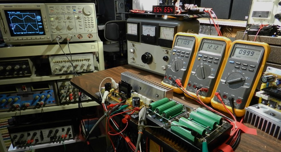
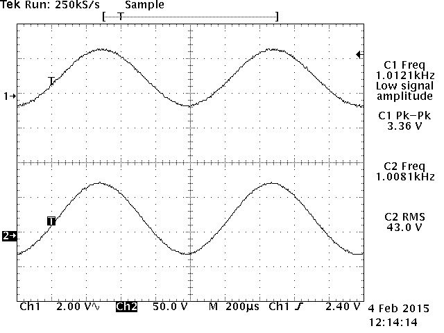
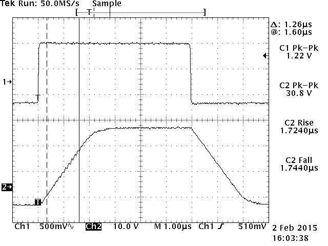
The power output was measured using an HP3312A Function Generator set at 3.36Vp-p sine wave and connected directly to the input of the amplifier, as well as the CH1 test probe of the oscilloscope. An 8Ω/700Watt dummy load was connected at the output of the amplifier under test as well as the CH2 test probe of the Tektronix TDS520D 500MHz DPO. The project’s prototype model produces a very nice sine wave of 43Vrms across the 8Ω/700W dummy load or a power output of more than 230 watts, as shown in the TEK hardcopy pictures above. The oscilloscope’s horizontal scale was adjusted at 200uS to verify for any visible clipping or artifacts on either peak. Enjoy!