Project 19
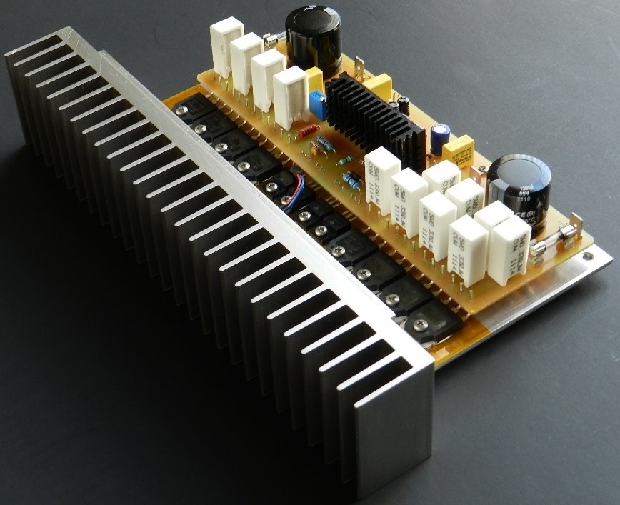
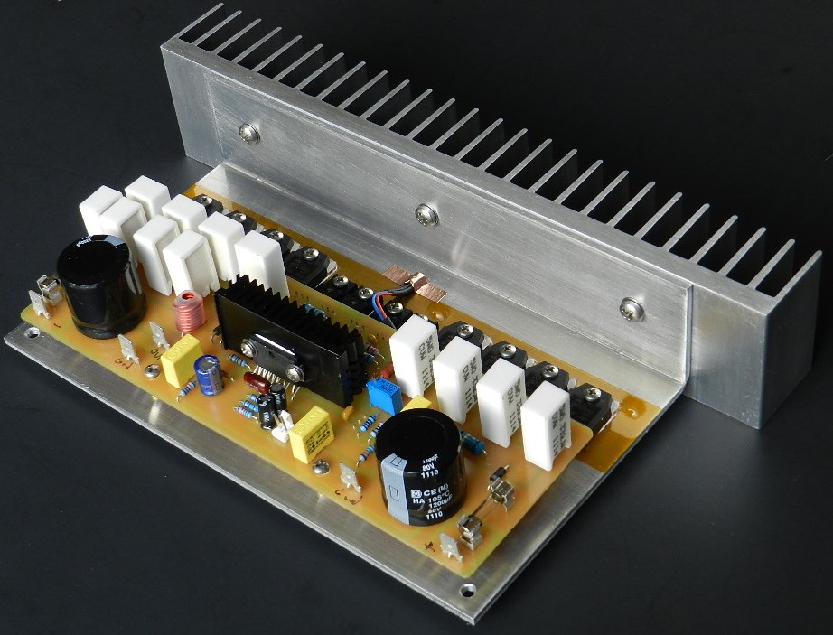
Project 19 is a classic quasi-complementary symmetry transistor output amplifier. There is only one complementary PNP transistor in the driver stage and the output stage consists of an all matched NPN power transistors. A Baxandall diode added at the emitter of the PNP driver transistor improves overall performance of the amplifier. Project 19 will further improve its performance by utilizing an LME49811 as the input stage. You might ask, why bother with an old type of power output configuration? Just consider this project as an implementation of an old circuit design complementing the outstanding features of the LME49811. Again, this type of power output topology might not be considered a practical choice for home use; it certainly deserves to be an alternative audio amplifier project of several channels of Project 19 for massive outdoor sound reinforcement applications. The power output for this project is about 275Wrms into an 8Ω load with a ±75VDC power supply.
The output stage schematic diagram, BOM and PCB layout for Project 19 are available for free by request, as is, no warranty.
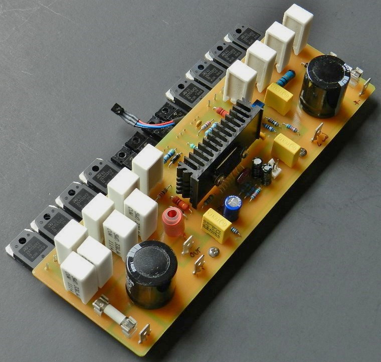
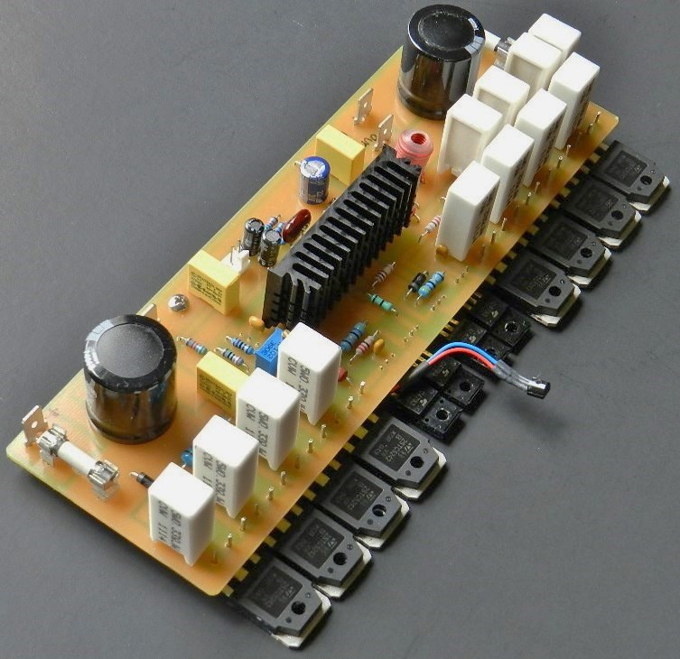
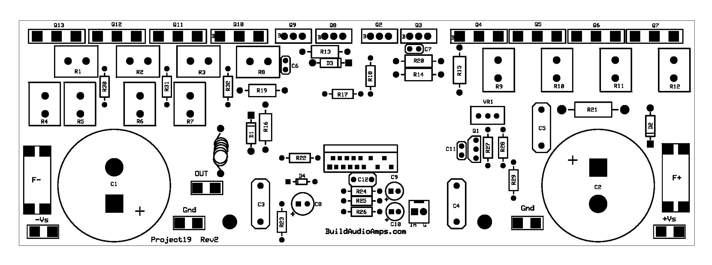 Project19 Silkscreen parts placement layer of PCB.
The following test procedure will use a higher power supply voltage than previous projects, so please be careful when performing the tests. Do not touch any part of the amplifier under test as well as the dummy load during power output measurement. Here comes the fun part. Prepare 2 DMMs to measure the DC offset voltage and idling current of the amplifier. Insert a jumper or shunt at the input of the amplifier. Do not connect any load or speaker at the output of the amplifier.
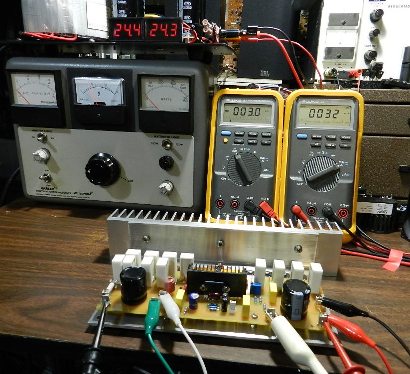
Initially adjust the Variac-controlled power supply to ±24VDC. The picture on the left shows the DC offset voltage at about 3mV measured at the output of the amplifier and the idle current at about 32mA across the F+ fuse terminals. Adjust VR1 to obtain this reading after a warm-up period of about 10 minutes. Switch the power supply to OFF immediately if you get different DMM readings. Proceed with the test procedure if you acquire the same DMM readings.
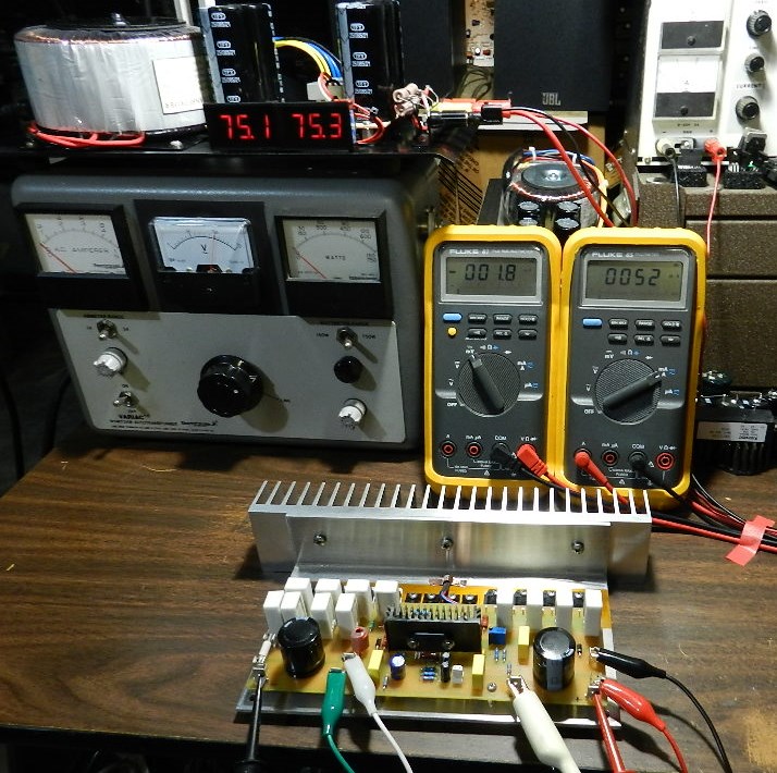
Gradually adjust the Variac to obtain ±75VDC from the power supply while keeping watch on any abnormal increase in the DMM readings. If you observed an increase in either DMM readings switch the power to OFF immediately before it vaporizes any component and check for PCB assembly errors. The picture on the right shows the DC offset voltage at about 1.8mV and the idling current at about 52mA. If you get the same DMM readings proceed and celebrate with music test.
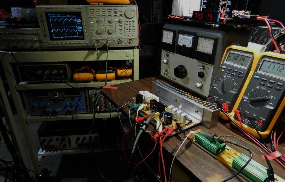

The next test procedure is optional, but if an oscilloscope, audio signal generator and 8Ω dummy load are available, you can measure the power output of the amplifier. The power output was measured using an HP3312A Function Generator set at about 1KHz 3.68Vp-p sine wave output and connected directly to the input of the amplifier under test as well as CH1 test probe of the oscilloscope. An 8Ω/400Watt dummy load was connected at the output of the amplifier under test as well as CH2 probe of the Tektronix TDS520D 500MHz DPO.
The amplifier produces 46.9Vrms across the 8Ω/400W dummy load or a power output of about 275Wrms, as shown in the TEK hardcopy picture. The horizontal scale was adjusted at 200uS to verify for any visible clipping on its peaks. An impressive power output of 550Wrms is possibly attainable with a 4Ω load. If you plan to connect a 2Ω load to Project 19, it will require additional NPN power output transistors, a bigger heat sink and forced air-cooling to produce a substantial power output of more than 1000Wrms. Enjoy!