Project 48

Project 48 is a high-powered fully symmetrical CFA-based audio power amplifier project. The prototype achieved a 100KHz square wave rise time of 770nS at 32.2Vpp, equivalent to a slew rate of 131V/uS. Decreasing the frequency to a more realistic 20KHz square wave signal, the rise time achieved was 903nS but the output amplitude reaches to as much as 50.4Vp-p, with negligible overshoots on either peaks. The slew rate at this frequency is about 175V/uS. Both test waveform results are shown in the Tek hardcopy pictures below.

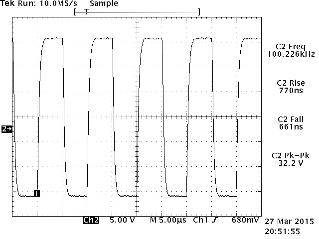
20KHz square wave rise time of 903nS at 50.4Vpp. 100KHz square wave rise time of 770nS at 32.2Vpp.
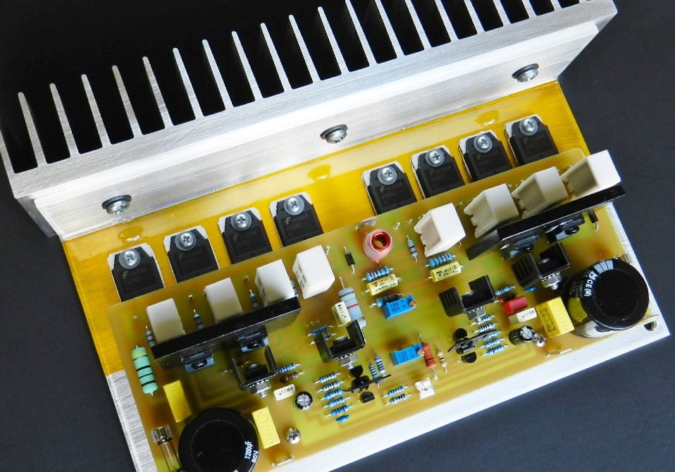
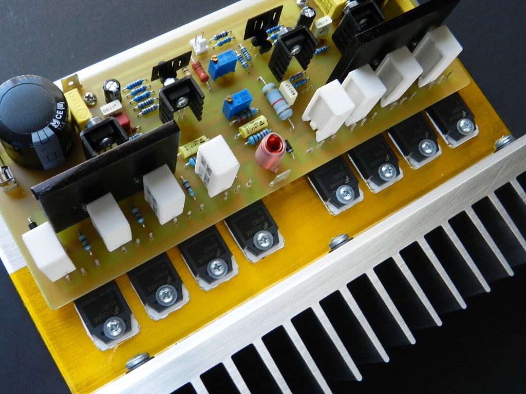
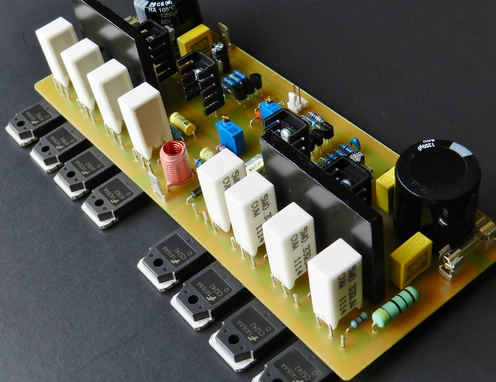
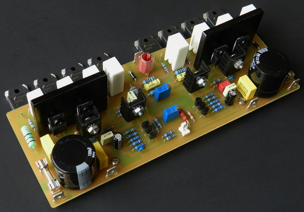
The prototype model was built on a 7.75” X 3.0” single-sided PCB. All components used in the prototype model are readily available standard parts. If you are interested in building this project and have read the Information and Policies section of this website, the schematic diagram, PCB layout (available only by request) and BOM are free, as is, no warranty.
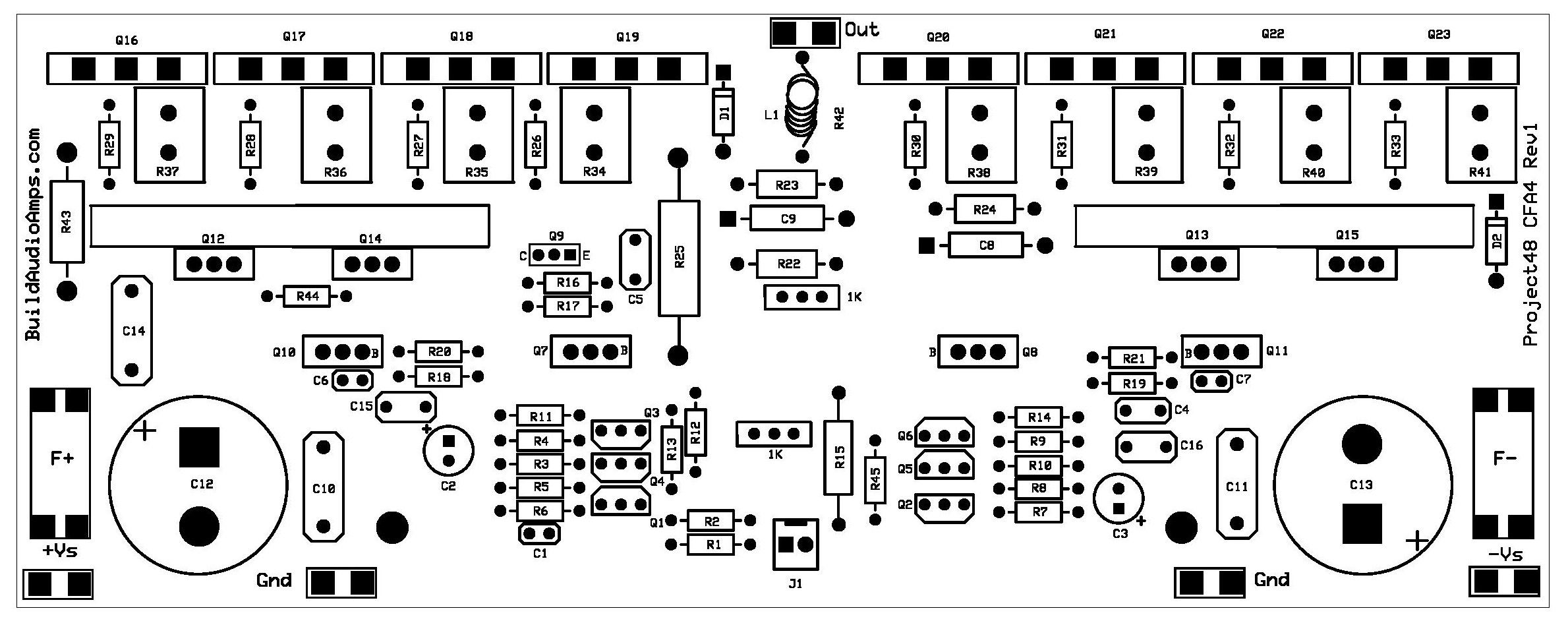
Project 48 Silkscreen Parts Placement Layer of PCB.
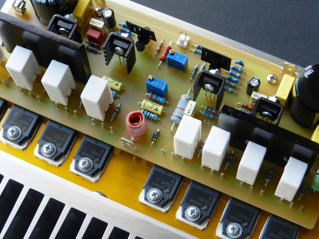
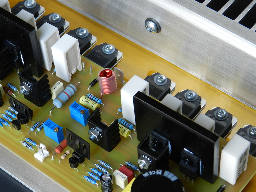
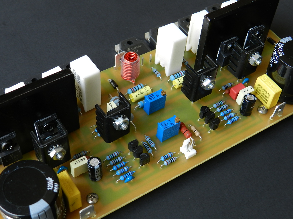
Please refer to the schematic diagram for a brief description of the circuit. The input signal at J1 is directly coupled and passes through a low pass filter consisting of R1 and C1 that suppresses unwanted RF noise from entering the complementary emitter-follower buffer stage transistors, Q1 and Q2. R2 supplies the base bias for Q1 and Q2 and its chosen value also reduces the overall DC offset voltage of the amplifier to minimum. The output of the buffers drives the summing stage transistors, Q4 and Q5. A feedback node consisting of R12 and R13 in parallel with VR1 sets the overall DC offset voltage of the amplifier by ±100mV. If optimum DC offset voltage is desired, an integrator op-amp similar to the one used in Project 4 can be implemented. However, in this project, there’s an improvement to the DC offset settling time because of the added cascode circuit to the error amplifier transistors. Negative feedback resistors, R15 and R25, are also tied to the same feedback node. These resistors determine the overall gain of the amplifier at 26dB.
The outputs of Q3 and Q6 are connected to the common emitter transistors, Q7 and Q8. A VBE circuit consisting of Q9, VR2 and other associated components sets the zero bias requirement of the output stage transistors. Frequency compensation capacitor, C4, is connected at the emitter of Q9 to signal ground.
The amplifier is equipped with a modified triple emitter-follower output stage. A complementary pair of T0126-packaged pre-driver transistors, Q10 and Q11, isolates the output of Q7 and Q8 from paralleled complementary T0220-packaged driver transistors, Q12//Q14 and Q13//Q15. Q10 and Q11 are frequency compensated by C6 and C7.The output of Q12 drives two paralleled TO3P-packaged NPN power output transistors, while Q14 drives another paralleled TO3P-packaged NPN power output transistors. The output of Q13 drives two paralleled TO3P-packaged PNP power output transistors, while Q15 drives another paralleled pair of TO3P-packaged PNP power output transistors. Utilizing four pairs of complementary power output transistors allows the amplifier to drive low impedance loads.
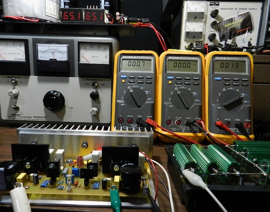
The amplifier requires approximately ±65VDC rails, produced from a rectified and filtered 90VCT at 300VA power transformer. The picture above shows a digital panel voltmeter reading of ±65.1VDC, obtained by connecting the AC input of the power supply to the AC output of a Variac transformer. Three DMMs are connected: at the output of the amplifier, across the emitter resistors, R37 and R41 and the overall current at F+ fuse terminals. The DMM on the left side of the picture shown above is measuring the DC offset voltage at 0.7VDC, which can be set by adjusting VR1. The DMM in the middle measures 0V across emitter resistors, R37 and R41; this can be acquired by adjusting VR2. The DMM on the right side of the picture is measuring the overall current across the F+ fuse terminals at 13mA.
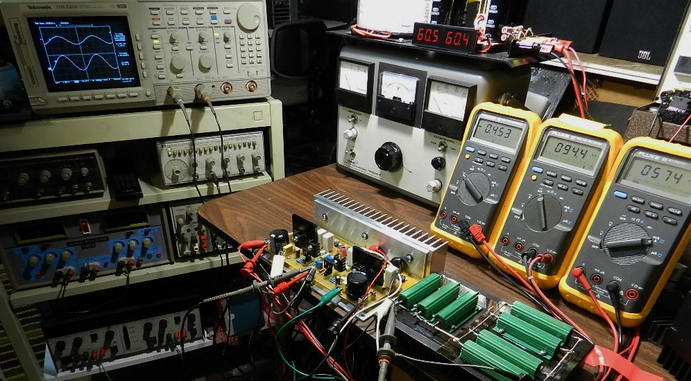
The picture below shows the test setup for power output and slew rate measurements. An HP3312A function generator and a Tektronix TDS520D 500MHz oscilloscope was used for these particular tests. However, similar equipment can be used, if you’re planning to perform the same optional tests. Be careful not to touch the amplifier under test, heatsink and dummy load; they will get very hot. The dummy load is only connected to the amplifier during initial testing and power output measurement. It should be disconnected from the output of the amplifier during slew rate measurement. The Zobel network resistor, R43, a 10Ω 3W wire wound power resistor, should be disconnected as well. Running a continuous 100KHz and 200KHz square wave signal to the amplifier will vaporize this resistor.
The measured power output of the amplifier before clipping is 205watts at 8Ω or 410 watts at 4Ω load with ±65VDC power supply rails. This power output was achieved by a 40.5Vrms across an 8Ω dummy load. Shown below are Tek hardcopy pictures of the output waveforms for an input sine wave signal at 4.8Vpp and 5.2Vpp respectively.
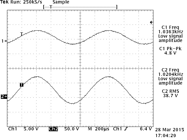

Power output at 187watts at 8Ω. Power output at 205watts at 8Ω.
“One of the worst-kept secrets in audio engineering is that what we hear does not always correlate with what we measure” – Richard C. Heyser
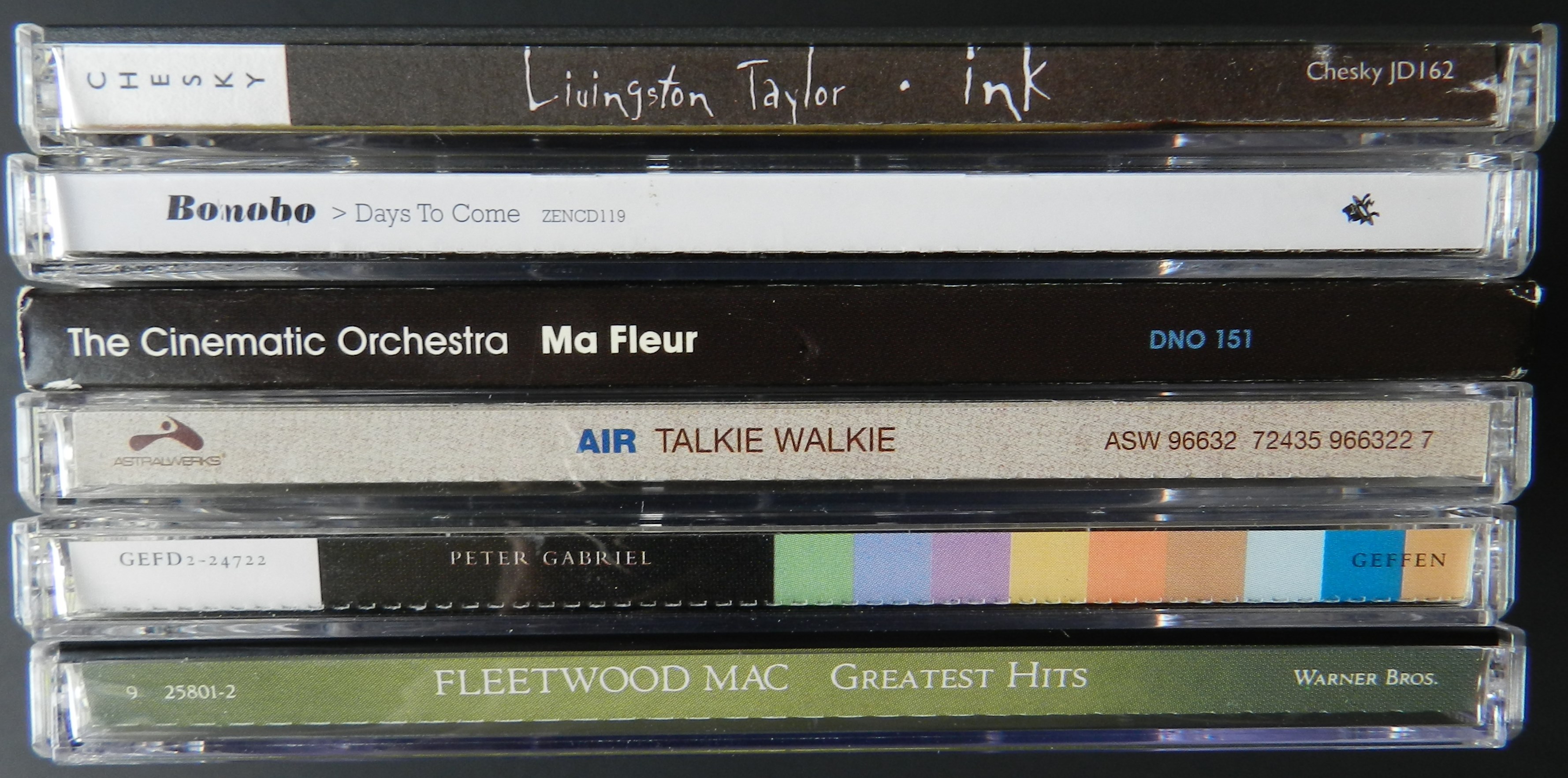
In real world listening with various music materials, the experience was amazing. The prototype unit was connected to a modified LM49720 tone control preamp. Listening to Livingston Taylor’s “Isn’t She Lovely” and “Get Here” from his “Ink” album, played on a Toshiba HD-A2 player and a Kenwood MV-9D monitor speaker, you hear impressive clarity of the audio frequency spectrum. The entirety of Bonobo’s “Days To Come” CD2 disc was also played with very good musical fidelity. Other CD albums shown above were also auditioned during listening test.