Project 50

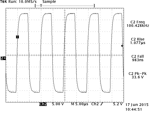
Project 50 is a MOSFET version of the fully symmetrical complementary Current Feedback Amplifier project. The project is implemented with a two-stage source-follower power MOSFET output stage. The prototype for this project achieved a power output of more than 200 watts at 8Ω with a ±64VDC power supply rails. Higher power output is possible with low impedance 4Ω load. The wide bandwidth characteristic of a CFA-based audio power amplifier produces a very good slew rate shown below at 25KHz and 100KHz respectively. The 25KHz square wave’s peak-to-peak amplitude adjusted at 102.4 volts produces a rise time of 699nS just before showing any signs of overshoots. The 100KHz square wave’s peak-to-peak amplitude was modestly adjusted at 28V volts resulted to a rise time at 1.080uS. The sonic performance during music test also reveals the spectacular attribute of a CFA-based audio power amplifier and perhaps one of the best sounding audio power amplifier projects built in the workshop!
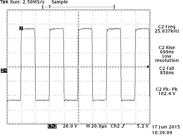
Slew Rate measurement at 25KHz Slew Rate measurement at 100KHz
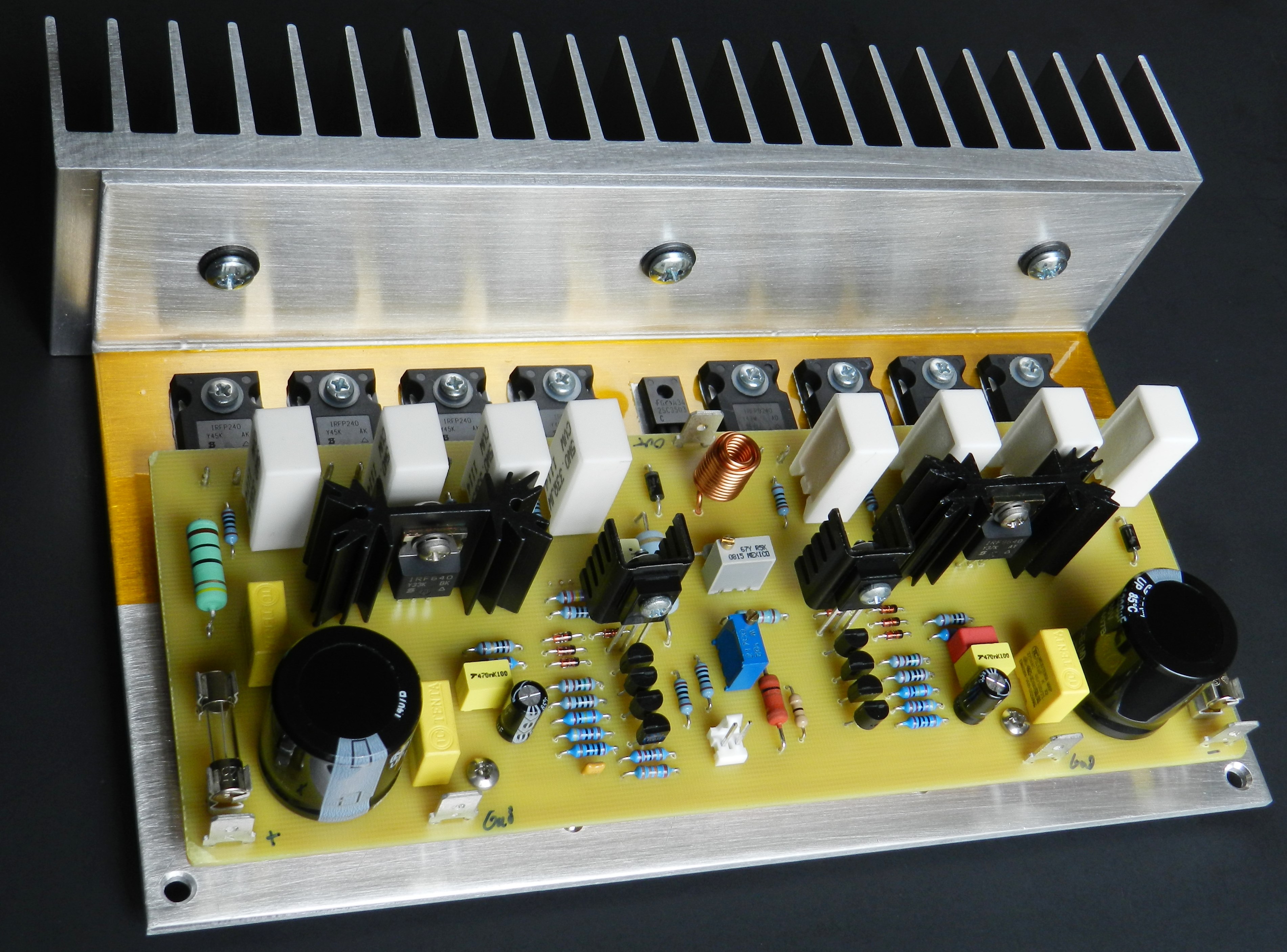
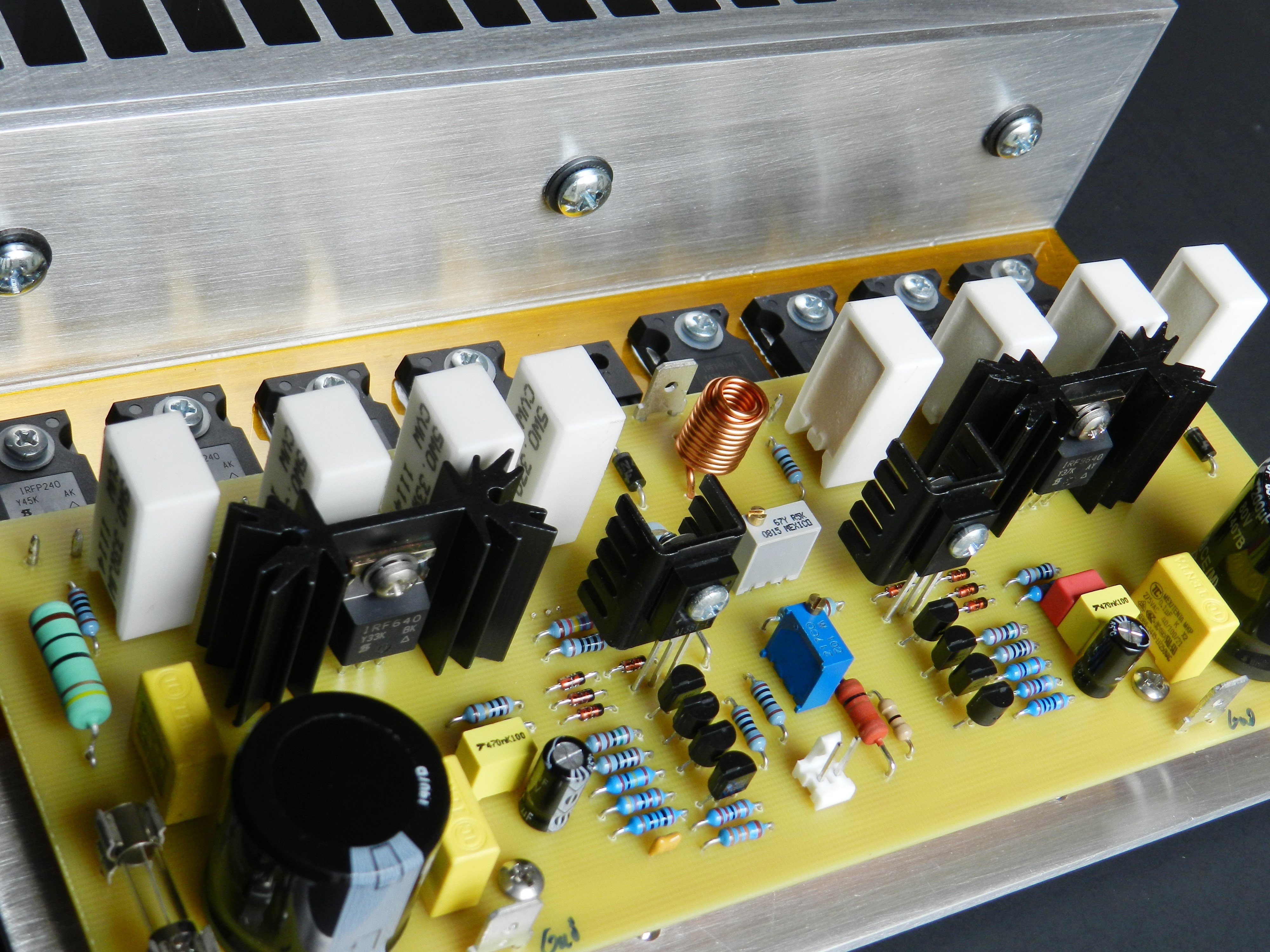
Please refer to the schematic diagram for a brief description of the circuit. The input signal at J1 is directly coupled and passes through a low pass filter consisting of R1 and C1 that suppresses unwanted RF noise from entering the complementary emitter-follower buffer stage transistors, Q1 and Q2. R2 supplies the base bias for Q1 and Q2 and its chosen value also reduces the overall DC offset voltage of the amplifier to minimum. The output of the buffers drives the cascoded summing stage transistors, Q4/Q3 and Q5/Q6. A feedback node consisting of R12 and R13 in parallel with VR1 sets the overall DC offset voltage of the amplifier by ±100mV. Negative feedback resistors, R15, and R42, are also connected in that same feedback node. These resistors determine the overall gain of the amplifier at about 26dB.
If optimum DC offset voltage is desired, an integrator op-amp similar to the one used in Project 4 may be implemented. However, there’s an improvement to the DC offset settling time in this project compared to previous CFA-based projects because of the additional cascode transistors to the error amplifier stage transistors.
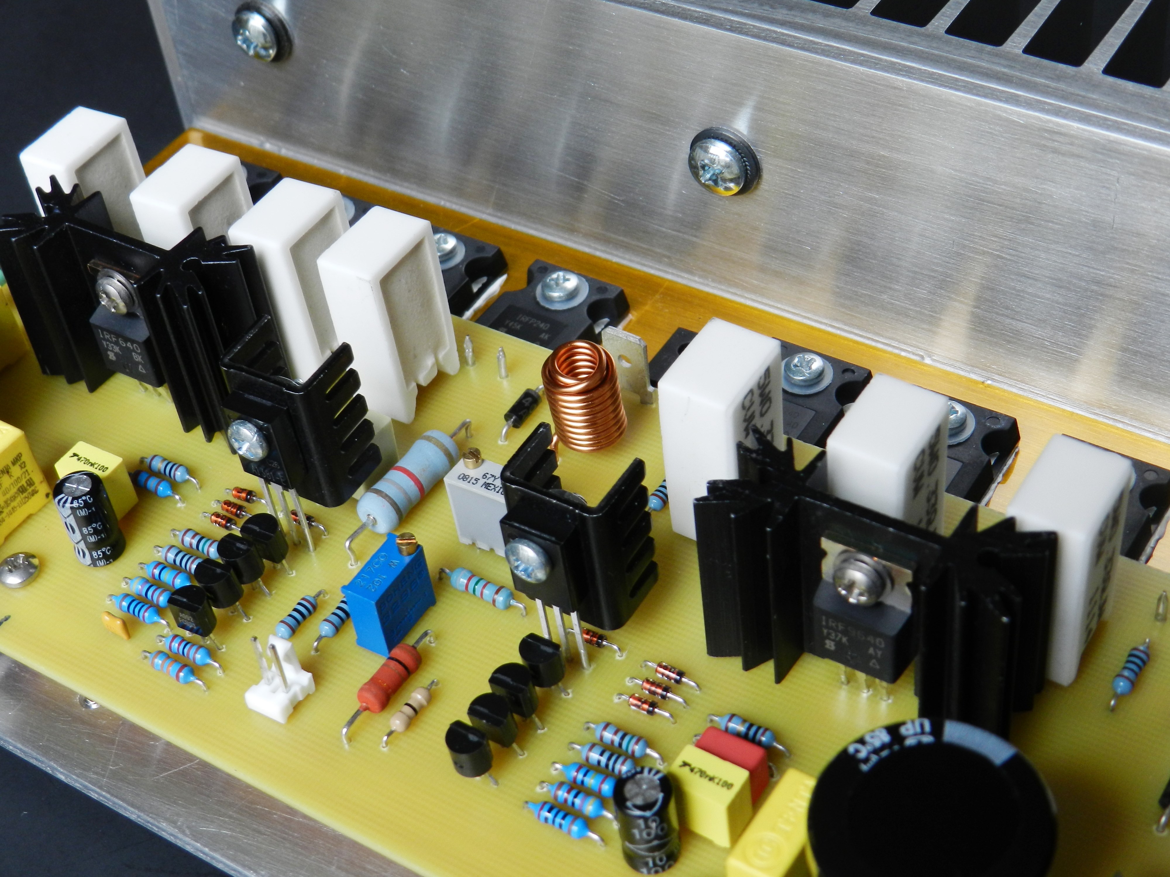
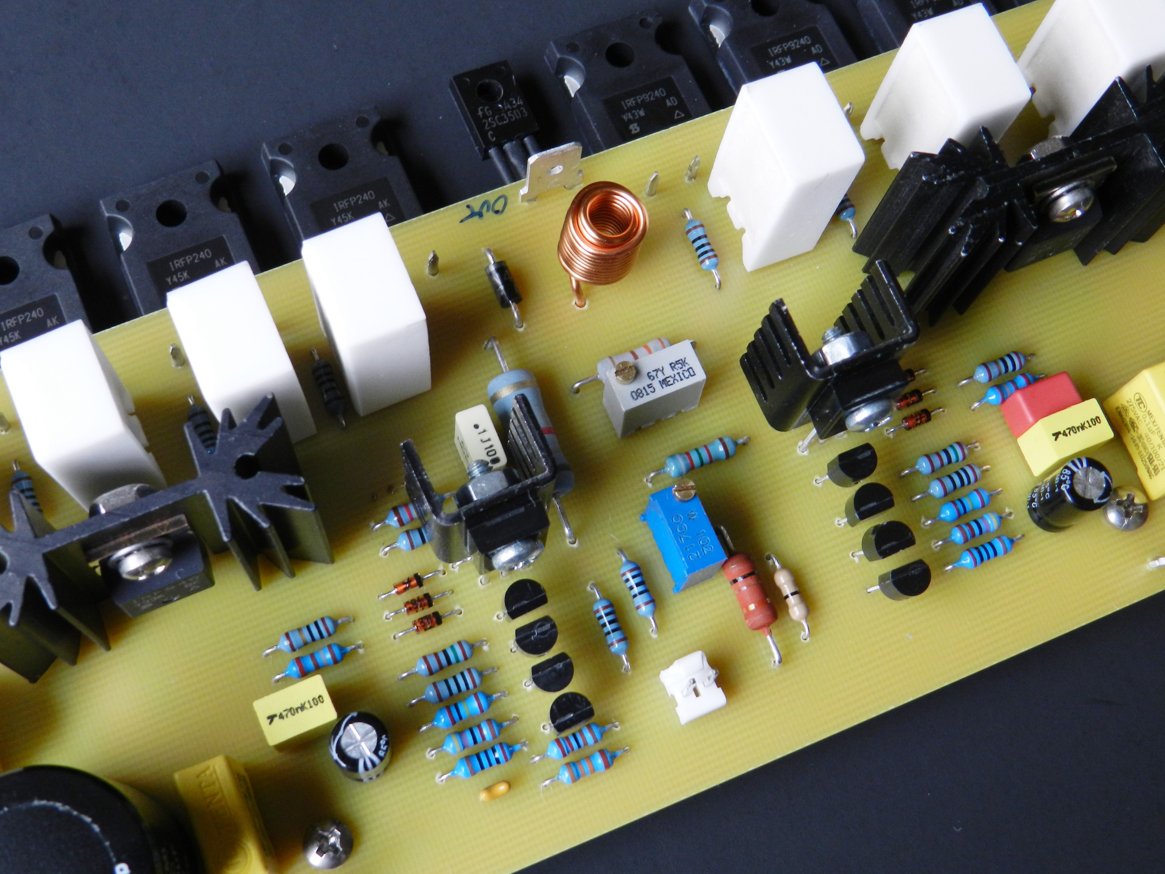
The outputs of Q3 and Q6 are connected to another cascode arrangement of Q7/Q8 and Q11/Q10. These allow better isolation of the outputs of the input stages from the pre-driver stages, improve actual measured slew rate and differentiate this project from prior CFA-based project. A conventional VBE circuit consisting of Q9, VR2 and other associated components sets the bias requirement of the output stage transistors. A frequency compensation capacitor, C4, is connected at the emitter of Q9 to signal ground. Q9 should be mounted in close proximity with the power output transistors. In the prototype, Q9 is mounted to the mounting bracket with a double-sided thermal adhesive.
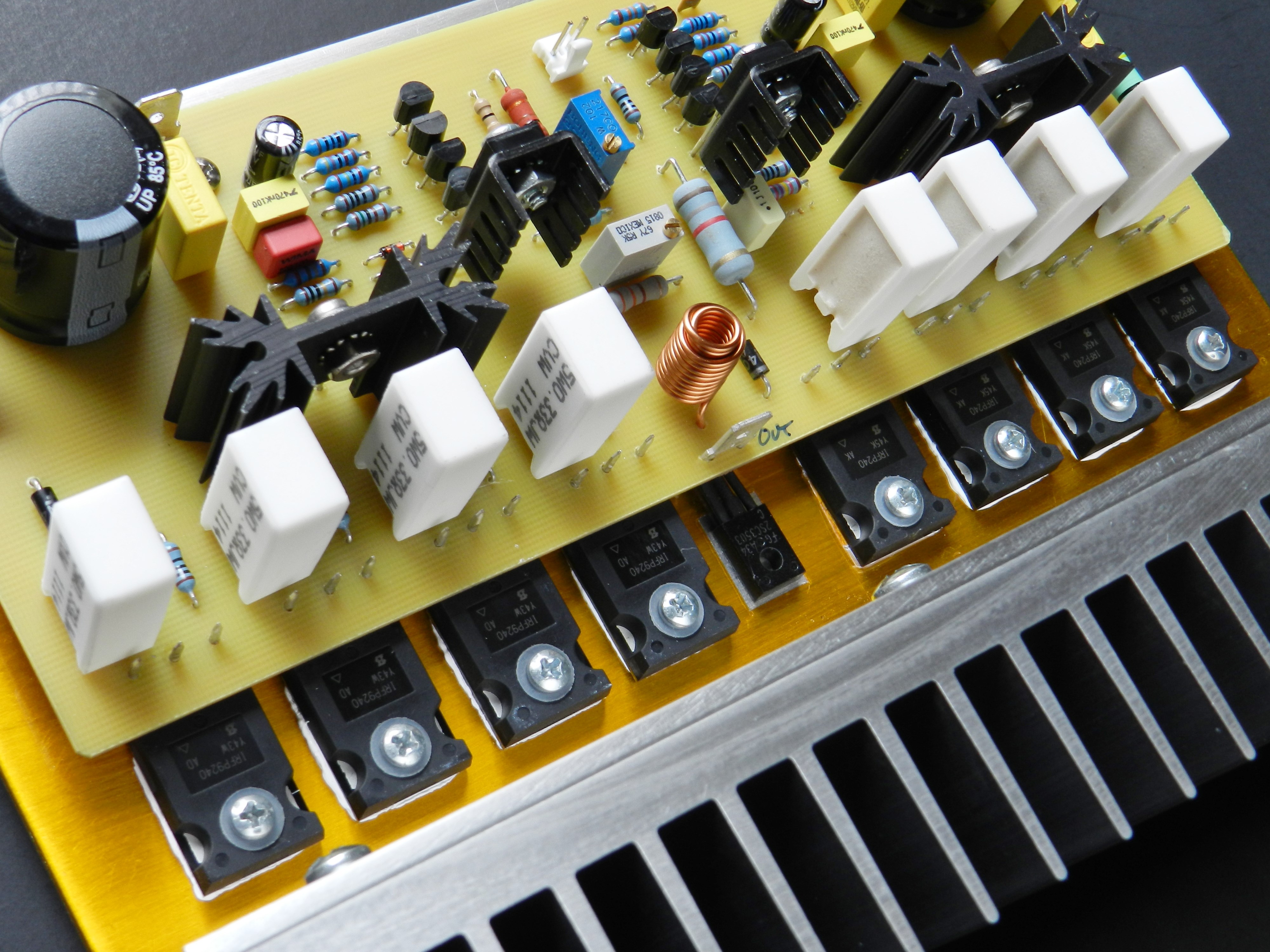
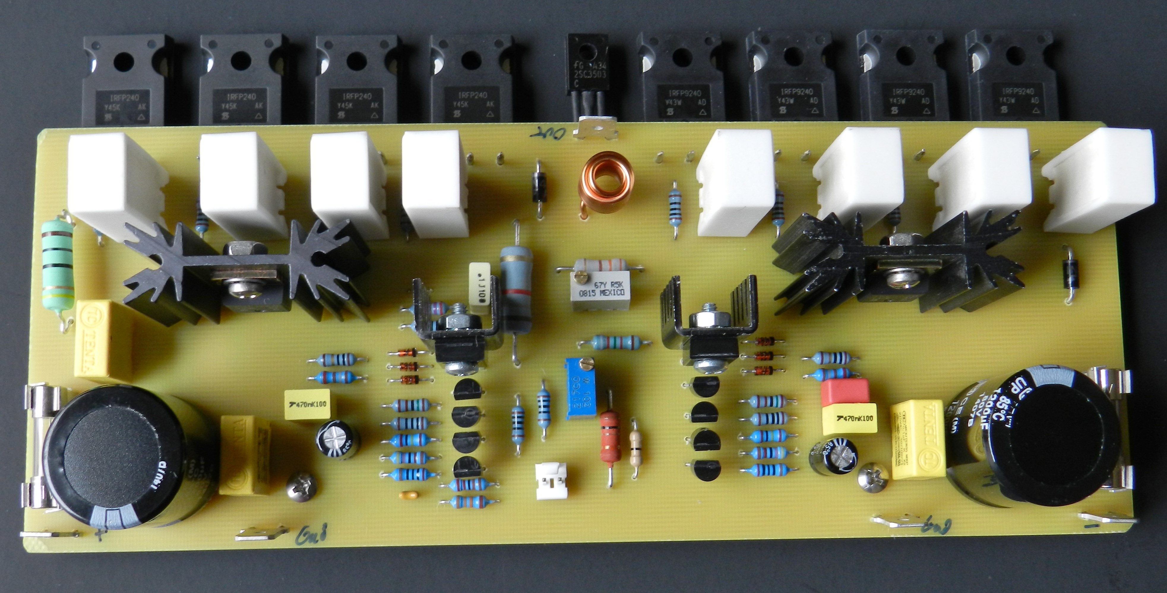
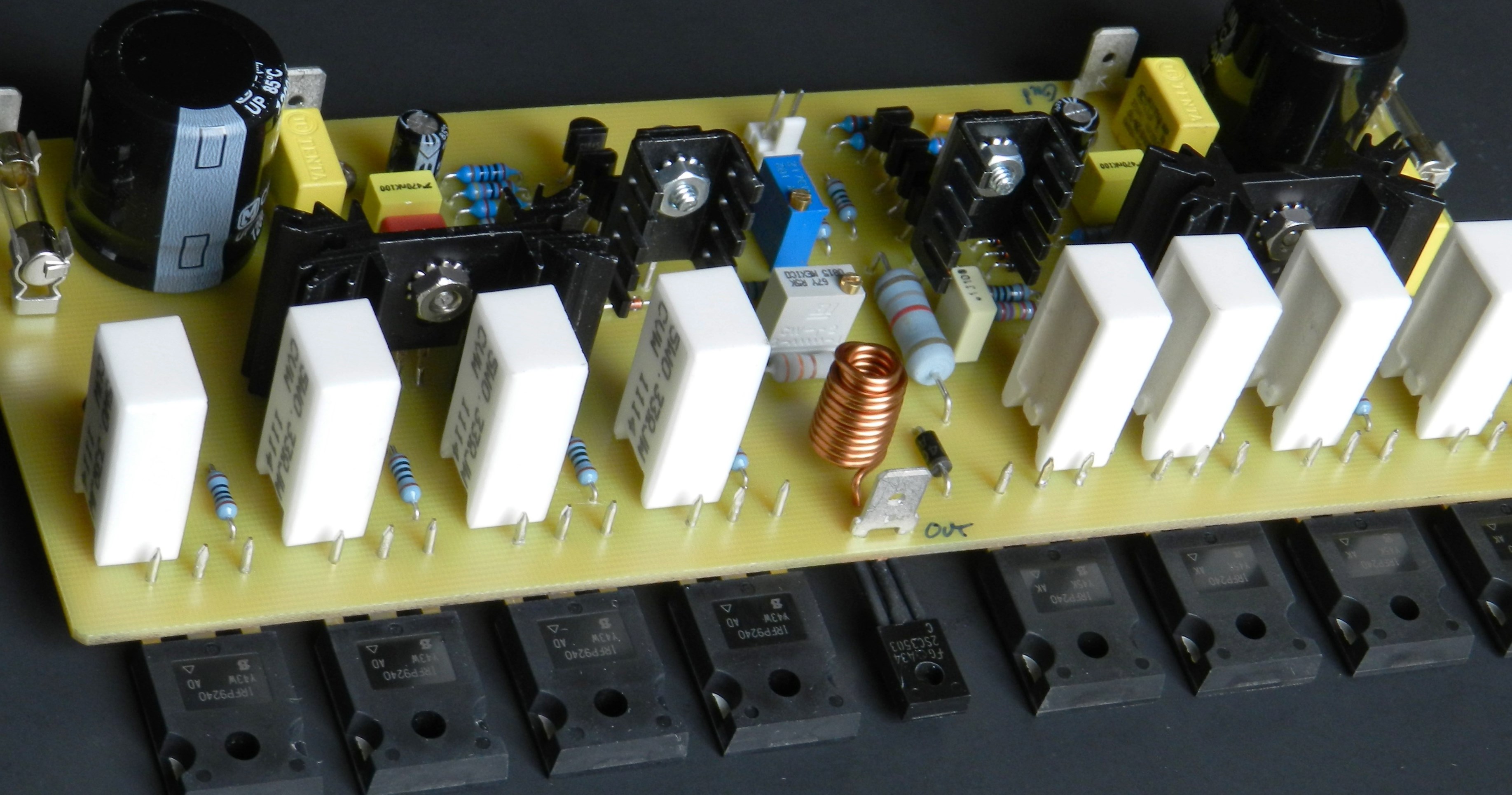
The output stage consists of a two-stage source-follower configuration. A complementary pair of T0220-packaged pre-driver MOSFETs, Q12 and Q17, isolates the output of Q8 and Q10 from the paralleled complementary output power MOSFETs, Q13 through Q21. Utilizing four pairs of complementary power output transistors allows the amplifier to drive low impedance loads. There’s no protection circuit that’s included in the prototype, however, the “uPC1237 Speaker Protection and Power ON Delay Project” may be implemented to this project for peace of mind. A simpler alternative is to use a 10-amp fuse in series with the main amplifier output and speaker. This protects the power output transistors from damage in case of accidental speaker cable shorts.
The prototype model was built on a 7.75” X 3.0” single-sided PCB. All components used in the prototype model are readily available standard parts. If you are interested in building this project and have read the Information and Policies section of this website, the schematic diagram, PCB layout (available only by request) and BOM are free, as is, no warranty.
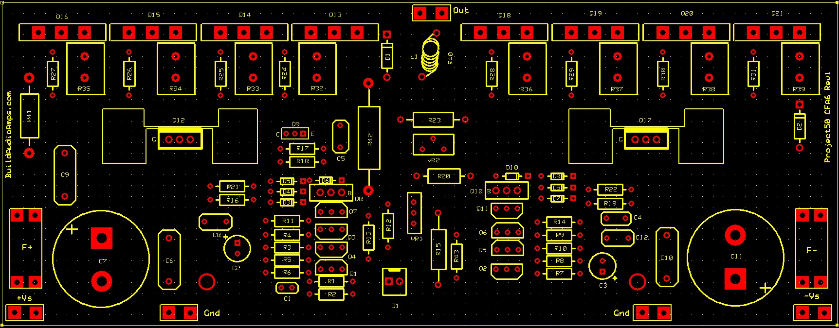 Project 50 Silkscreen Parts Placement Layer of PCB.
Before powering up the project, check the very high resistance ohmmeter reading (greater than 1MΩ to ∞) between drain of all power MOSFETs and the aluminum mounting bracket/heatsink. Apply a generous amount of heatsink compound to these transistors as well.
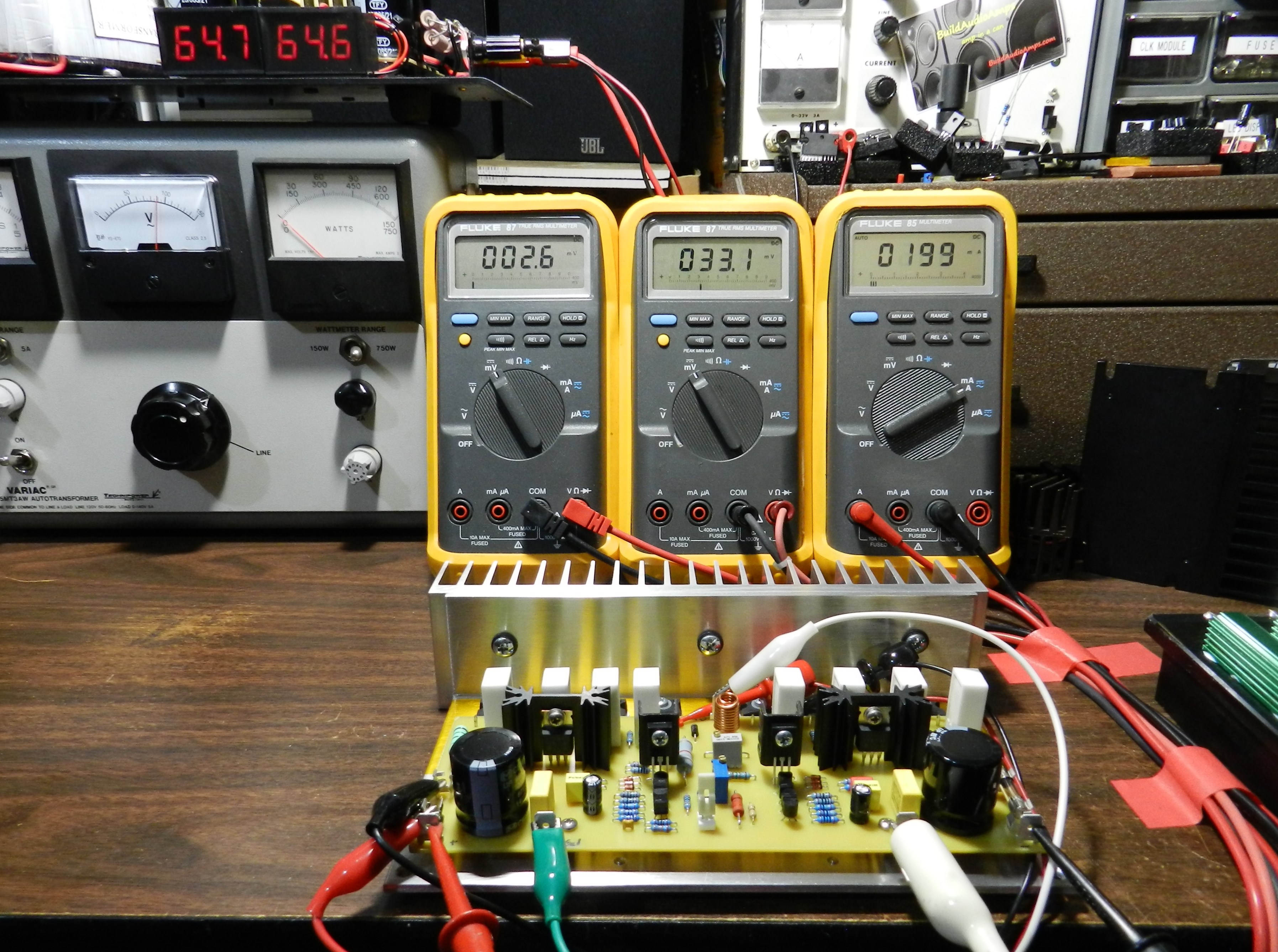
The amplifier requires approximately ±64VDC power supply rails; produced from a rectified and filtered 90VCT at 300VA power transformer. The picture above shows a digital panel voltmeter reading at approximately ±64VDC, obtained by connecting the AC input of the power supply to the AC output of a Variac transformer. Gradually adjust the Variac transformer so that the panel voltmeter reads from 0V to about ±65VDC while observing the DMMs: connected at the output of the amplifier, across the source resistors, R32 and R36 and the overall current at F+ fuse terminals. Power off immediately if you have noticed higher DMM reading other than what’s shown in the picture. Check the PCB for any possible assembly errors before powering up the amplifier again.
After the fault was determined and corrected, reapply power and allow the amplifier under test to warm up for more than 15 minutes before making any adjustments to VR1 and VR2. The DMM on the left side of the picture is measuring the DC offset voltage at 2.6mVDC, which can be set by VR1 and this could be adjusted as close to 0mV as possible. The DMM in the middle measures 33.1mV across any source resistors, R32 through R39; this is set by VR2 and it could be anywhere from 25mV to 35mV depending on the builder. The DMM on the right side of the picture is measuring the overall current across the F+ fuse terminals at 199mA and is dependent on the setting of VR2.
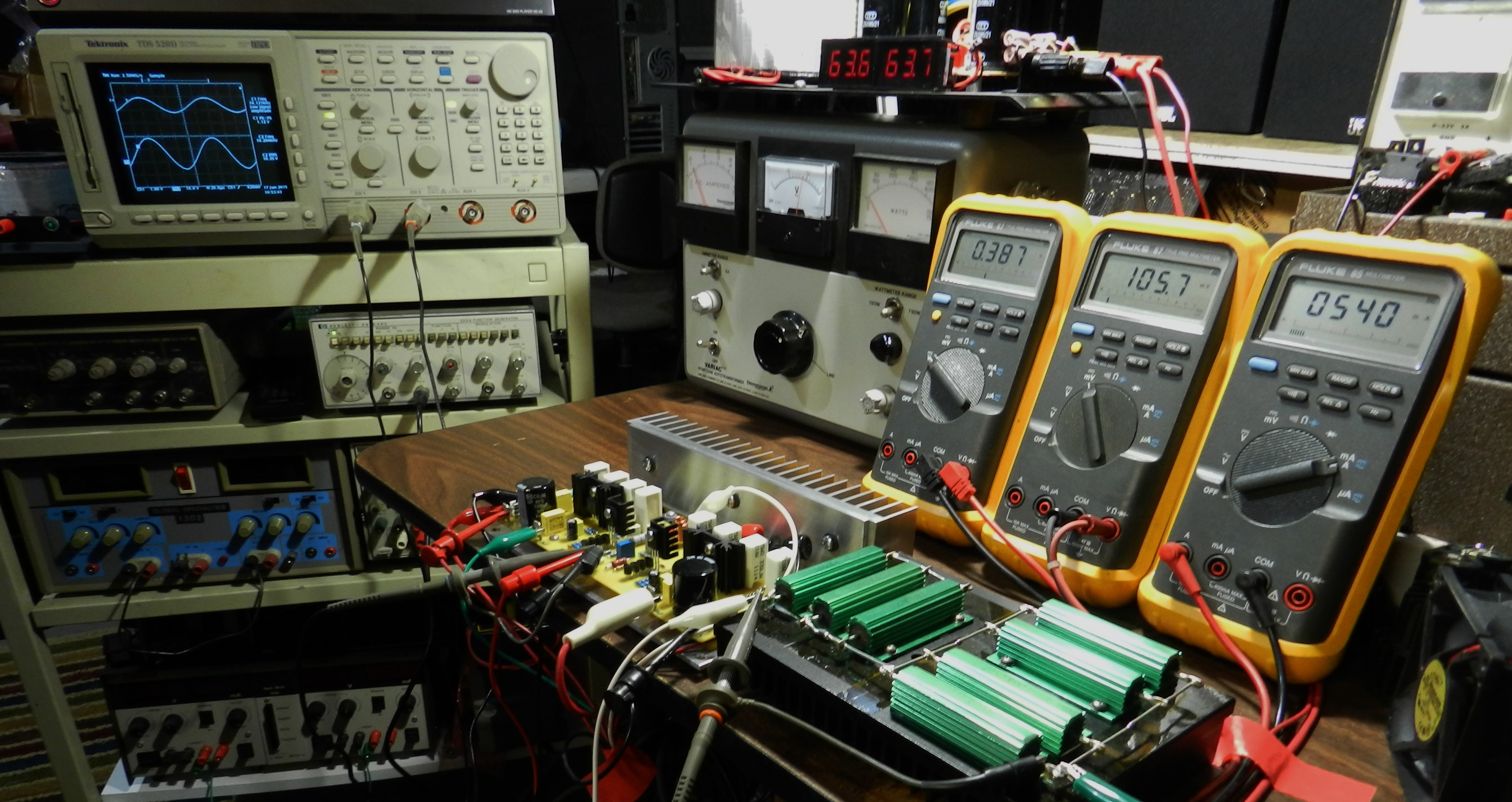
The picture on the left above shows the test setup for power output and slew rate measurements. Be careful not to touch the amplifier under test, heatsink and dummy load; they will get very hot! An HP3312A function generator and a Tektronix TDS520D 500MHz oscilloscope was used for these particular tests. However, similar equipment can be used if you’re planning to perform the same optional tests. The dummy load is only connected to the amplifier during power output measurement. It should be disconnected from the output of the amplifier during slew rate measurement. The Zobel network resistor R41, a 10Ω 3W wire wound power resistor, should be disconnected as well. Running a continuous high frequency square wave signal to the amplifier will burn-up this resistor.
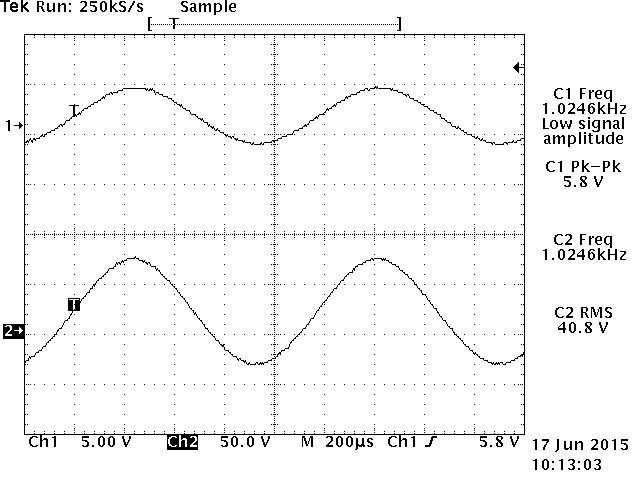
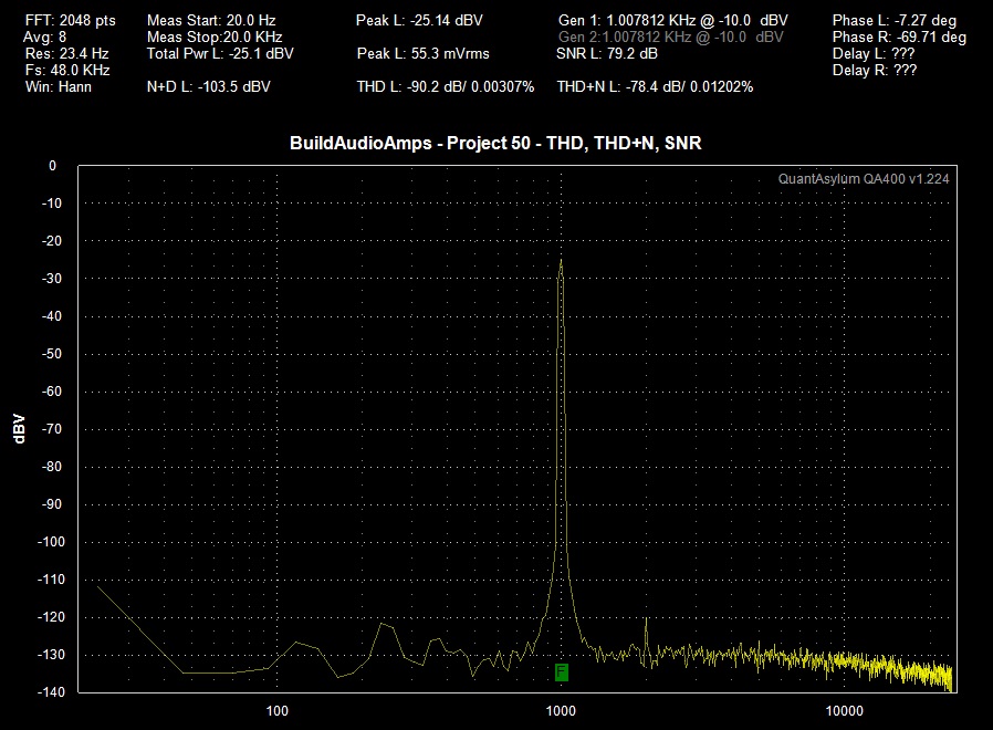
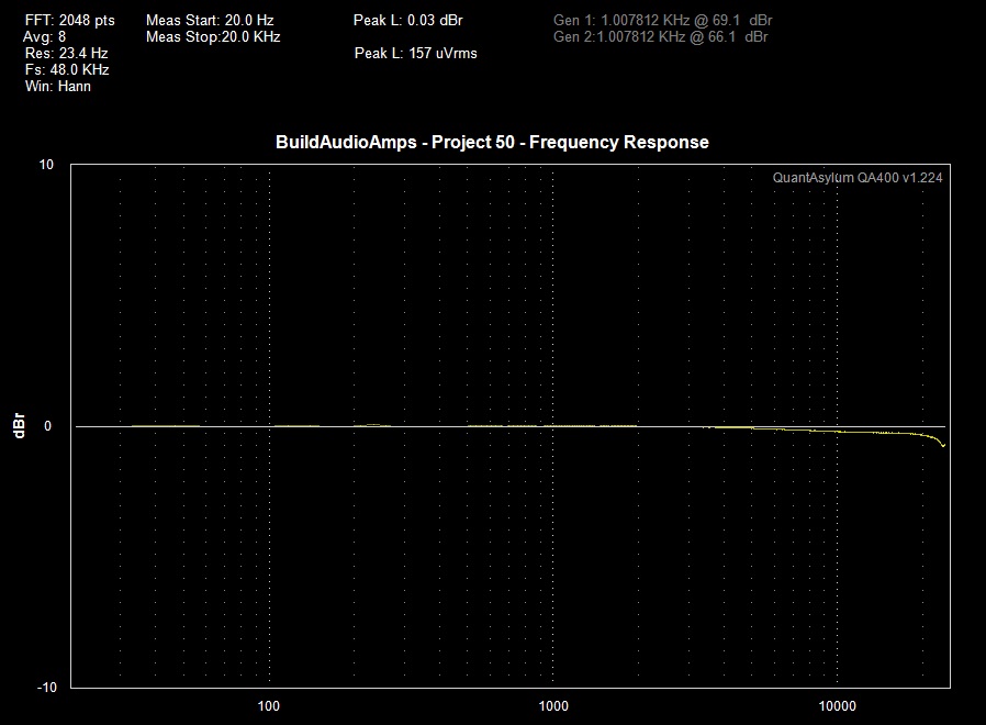
The measured power output of the amplifier just before clipping is 208watts at 8Ω with ±64VDC power supply rails. This power output was achieved by applying a 1KHz at 5.8Vp-p sine wave input signal to the amplifier that resulted to a 40.8Vrms across an 8Ω dummy load. The Tek hardcopy picture of the power output test result is shown above on the right. Shown earlier are Tek hardcopy pictures of the slew rate measurement output waveforms. These were obtained by applying a 25KHz and 100KHz square wave signal to the input of the amplifier and was adjusted so that the output amplitude does not show any overshoots on its peaks at 102.4Vp-p and 28Vp-p respectively. A QA400 Audio Analyzer and a QA190 Differential Probe were utilized to measure some basic parameters of interest and the test results are shown in the next pictures.
“Perhaps more than any other discipline, audio engineering involves not only purely objective characterization but also subjective interpretations. It is the listening experience, that personal and most private sensation, which is the intended result of our labors in audio engineering. No technical measurement, however glorified with mathematics, can escape that fact” – Richard C. Heyser

In real world listening with various music materials, the experience was very impressive. The prototype unit was connected to a modified LM49720 tone control preamp, a Toshiba HD-A2 player and a Kenwood MV-9D monitor speaker. Listening to B-Tribe’s “Adagio in G-Minor” from “Spiritual, Spiritual” album, you hear deep lows, extended highs and impressive mids as well. NPR’s Discover Songs series featuring “The New Jazz Divas” album was also played especially tracks 5, 6, 10 and 11 with very good musical fidelity. The entirety of Enigma’s “The Greatest Hits” album was also played for endurance testing. Other CD albums shown above were also auditioned during listening test.