
Project 14

After the completion of Project 13 another interesting subject came into mind: What if the driver and output transistors were rearranged to work in parallel instead of series-connected devices. Doing so will eliminate the bulky voltage divider 5W-resistors off the PCB. Is there such a design to be found on the web? The answer is Project 14.
The output stage circuit of Project 14 was inspired by a vintage NAD power amplifier product that was manufactured in 1998, the S200. The S200 is rated at 225W at 8Ω with about ±72VDC main power supply. The original NAD design utilizes an op-amp servo circuit to control the DC offset voltage of the amplifier, similar to Project 4. As a starting point I’ll use TI’s recommended value of feedback resistor (Rf) since the servo circuit will not be included in this project, sorry. Here’s the schematic diagram of the output stage circuit of Project 14:
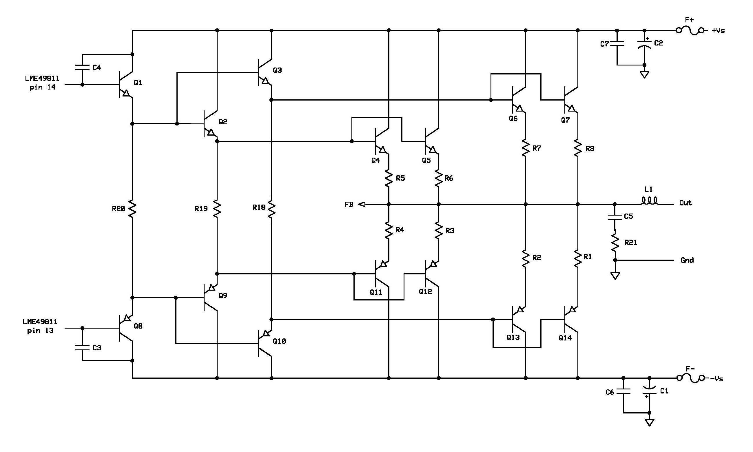
Transistors Q1/Q8 are configured as full complementary emitter follower pre-drivers for the parallel-connected Q2/Q3 and Q9/Q10 drivers. This circuit configuration is similar to a typical industry standard T-circuit, developed by Bart Locanthi in the late ‘60s. But here’s the kicker, the base of Q2 and Q3 are connected together while each emitters are driving independently the power output transistors Q4/Q5 and Q6/Q7 for the positive half of the amplified signal. The same goes with the negative half, the base of Q9 and Q10 are connected together while each emitters are driving separately Q11/Q12 and Q13/Q14. Very interesting!
The schematic diagram of the LME49811 input stage circuit is similar to previous projects but the Part IDs and some values were changed to match with the output stage as shown in Project14 BOM.

Let’s go ahead, build and test this project. Be sure to cut-to-length 2 pieces of 18AWG hook-up wires, strip and solder each end to J2 and J3. I’ve soldered those hook-up wires on the bottom copper layer of PCB. The guesstimated values of R29 and R26 was determined by t&e and listed in the bill of materials. The PCB layout and BOM are provided for free, as is, no warranty.
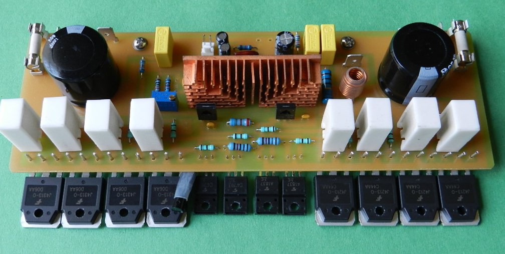
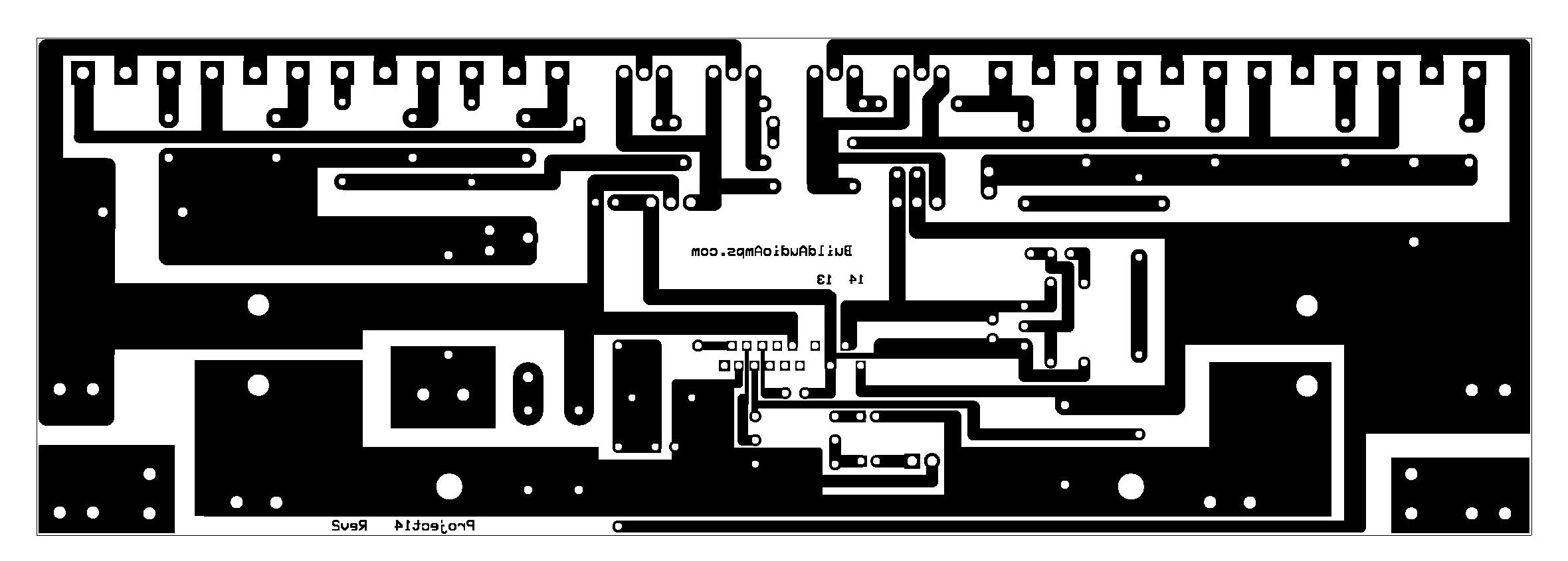
 Silkscreen Parts Placement Layer of the PCB for Project 14.
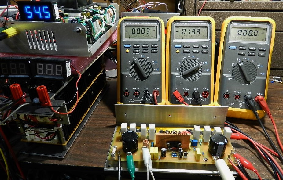
For initial testing, a ±24VDC power supply will be used, just to be safe! Install a shorting jumper at input J1 and do not connect any speaker at the output but a millivoltmeter. Remove F+ fuse and replace that with a milliammeter. Adjust VR1, a 1KΩ multi-turn variable resistor, counterclockwise for minimum resistance or until it clicks.
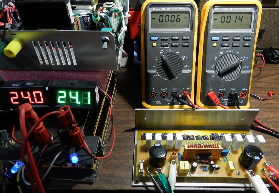
Switch the power supply to ON. The DMM on the left side of the picture is connected at the output and ground terminals of the amplifier. It reads about 0.6mV, the DC offset of the amplifier. The DMM on the right side of the picture is connected at the F+ fuse terminals. It reads about 14mA, the current drawn by the amplifier. The DMM readings are acceptable and you may proceed with music test, but if you obtain odd DMM readings, switch the power supply to OFF immediately and check for PCB assembly errors.
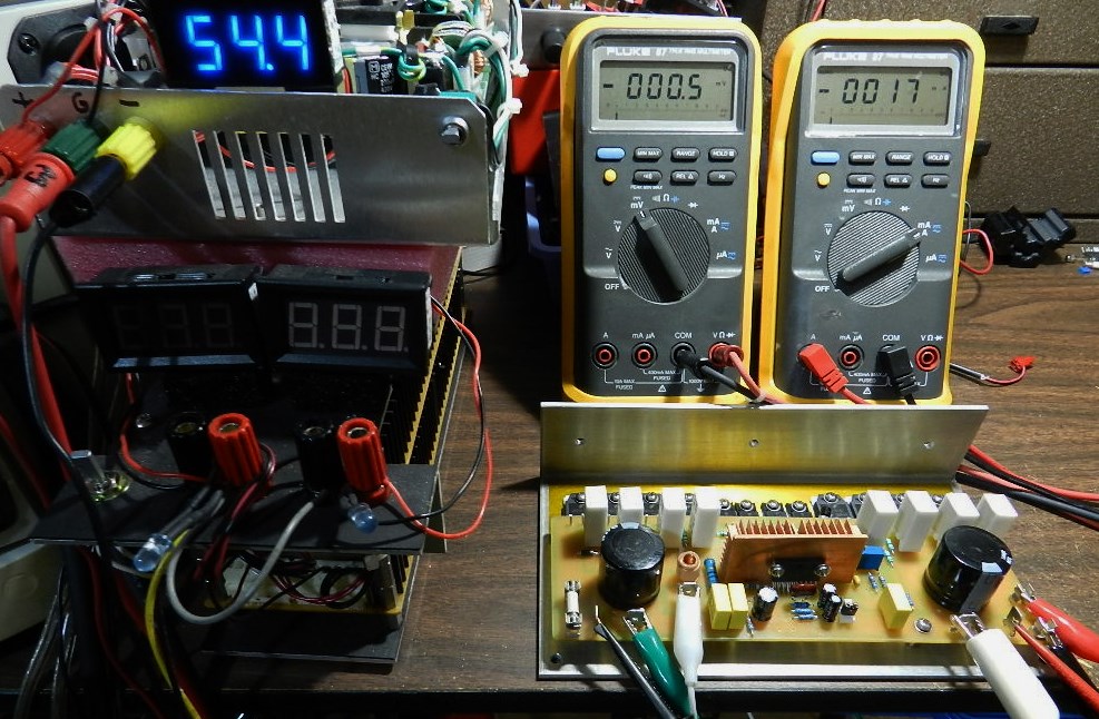
The picture shown above is using a ±54VDC test power supply, but this time the DC offset voltage is about 0.5mV and the current drawn is about 17mA.
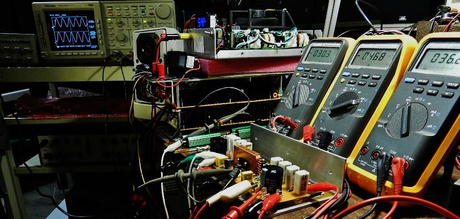
The next step is to adjust the idle current of the output transistors. With the power OFF, connect another millivoltmeter to the emitter of Q7 and output terminal, as shown in the preceding picture. The millivoltmeter will be measuring the voltage drop of R8. The voltage drop multiplied by the value of the emitter resistor is the idle current of the output transistors. Switch power supply to ON. Wait for about 15 to 30 minutes before adjusting VR1 clockwise to read about 8mV on the millivoltmeter and about 133mA on the milliammeter connected at the F+ fuse terminals. If you got that right, proceed with music test!
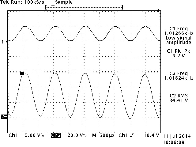
This next test is optional, but if you have an oscilloscope, audio signal generator and 8Ω dummy load, the power output of the amplifier can be measured. If not, the following pictures will show you those test results. It is recommended to add a small fan to cool down the amplifier under test and dummy load, it does get hot!
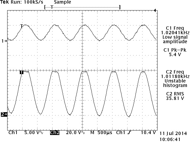
The picture on the left shows an input sine wave signal of about 1KHz at 5.2Vp-p that was applied into the amplifier under test and it produced about 34.41Vrms across the 8ohm/400W load or a power output of about 148Wrms. Increasing that same input signal to 5.4Vp-p, produced about 35.81Vrms across the same load or a power output of about 160Wrms, with slight clipping on the positive peaks. Enjoy!

![]()