Project 28


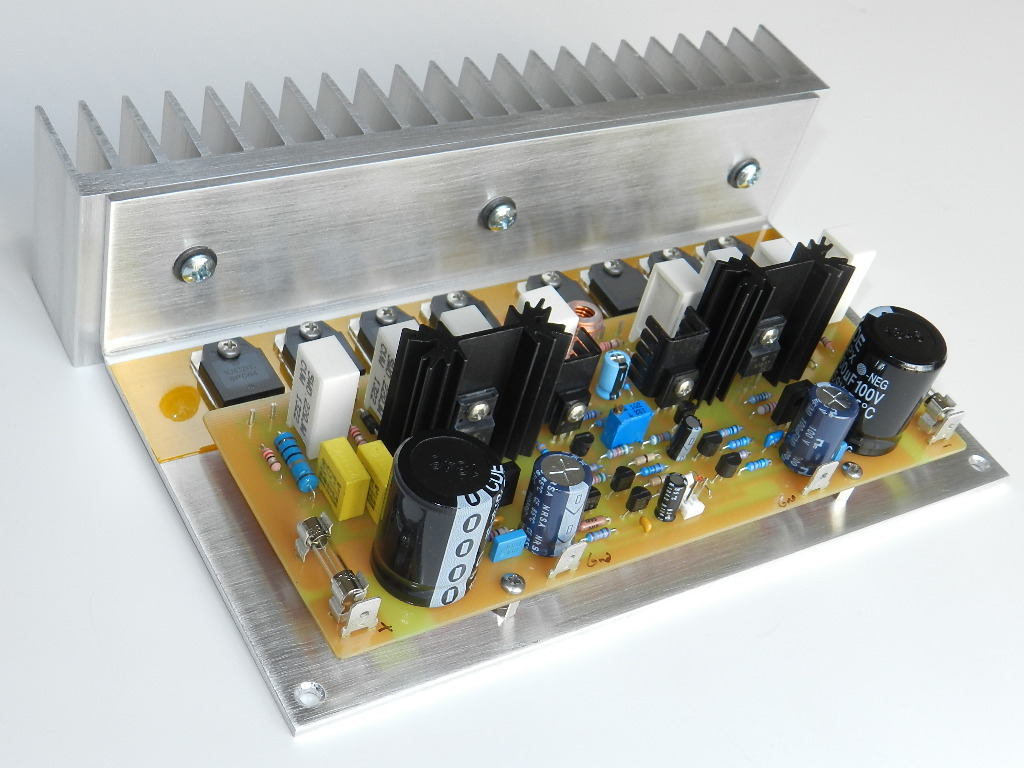
Project 28 is an updated version of Project 6. The measured power output of Project 28 is about 238W at 8Ω with a ±65VDC to ±70VDC power supply. The updated changes were made to the transistor part numbers used in the differential input stage, voltage amplifier stage as well as in the power output stage. The replaced complementary power output transistors have excellent features like exceptional safe operating area and excellent gain linearity. It also provides reliable performance at higher power, accurate reproduction of input signal, greater dynamic range and high amplifier bandwidth.
The major change of Project 6 is at the output stage section, which was converted into a three-stage T-circuit topology to achieve more current gain in driving low impedance loads while improving previous audio performance. The pre-driver and driver both have shared emitter resistors operating in Class A mode. No changes were made to the basic current-source, LTP, current-mirror front-end circuitry as well as the EF buffered voltage amplifier stage.
If you are interested in building this project and have read the Information and Policies section of this website, the updated schematic diagram, PCB layout (available only by request) and BOM for Project 28 are free, as is, no warranty.
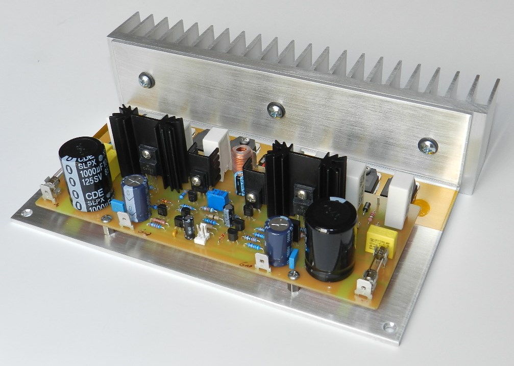
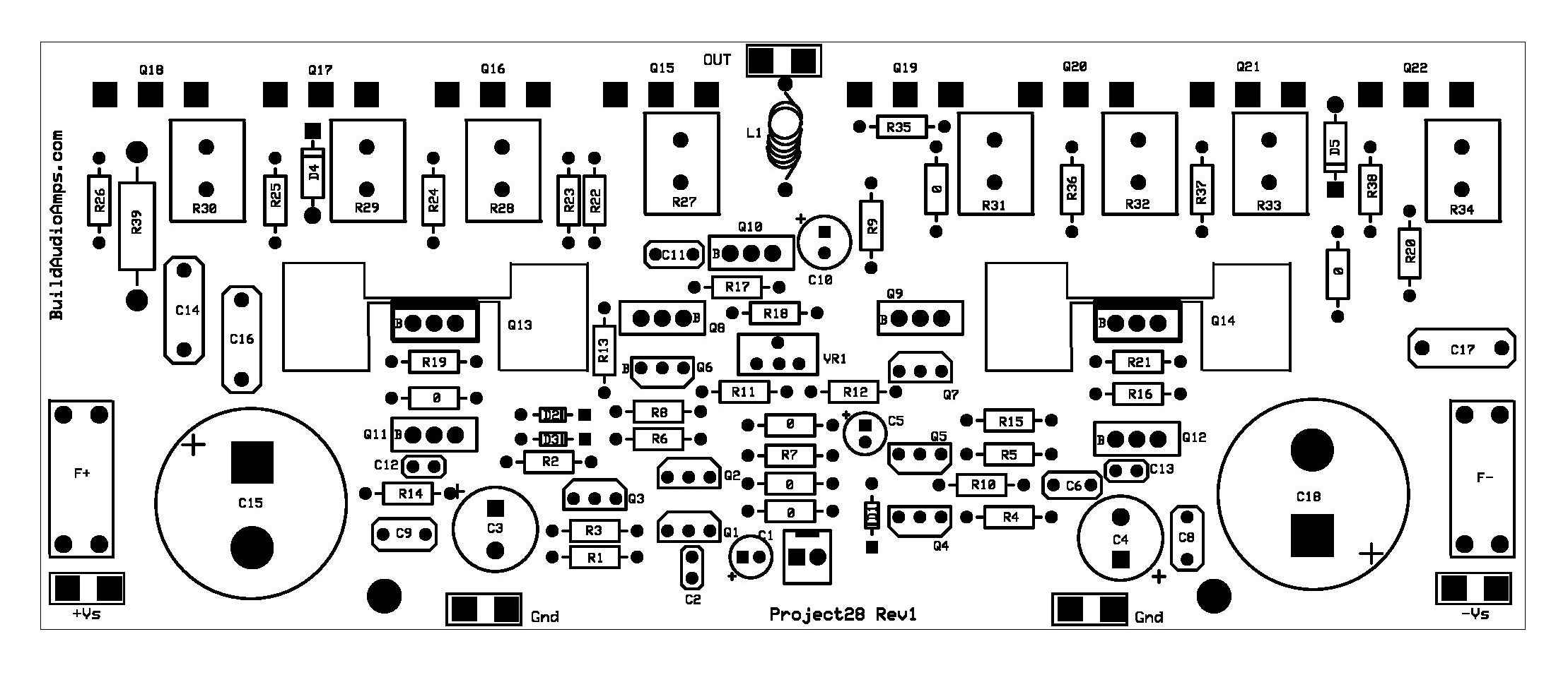 Silkscreen parts placement layer of PCB for Project 28.
A safe way of powering up your newly built project the very first time is to use a ±24VDC power supply or whatever low-voltage dual-polarity power supply that you may have. Project 28 was tested with a ±12VDC power supply and the audio fidelity at average listening level was surprisingly good without perceived distortions.
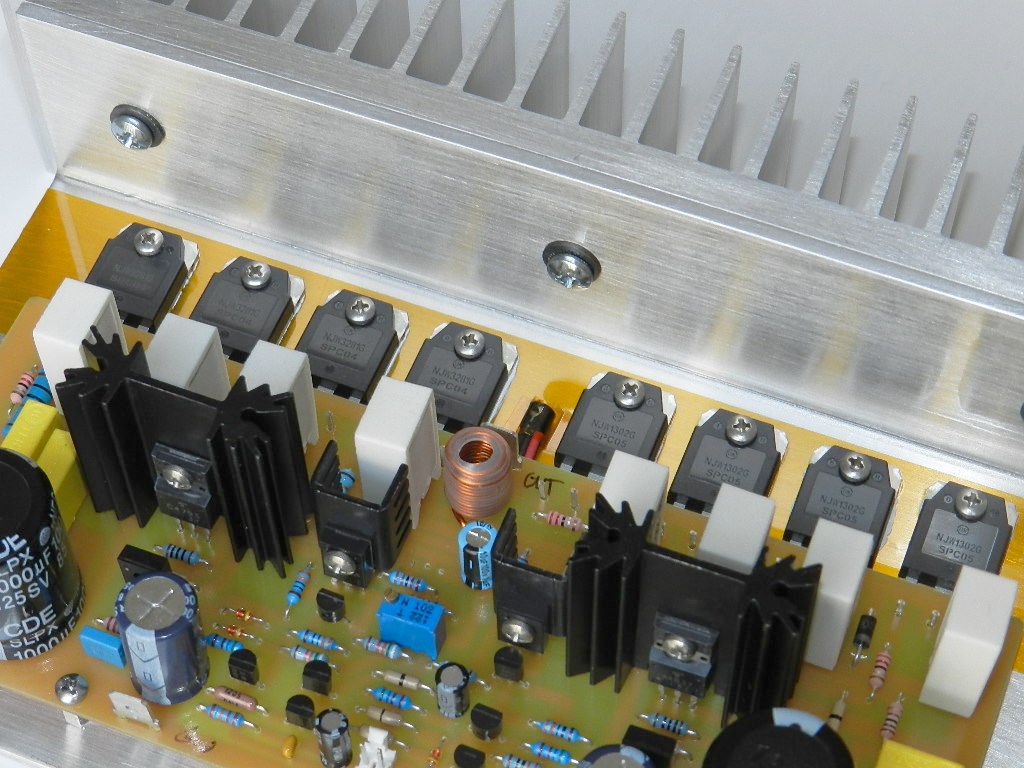
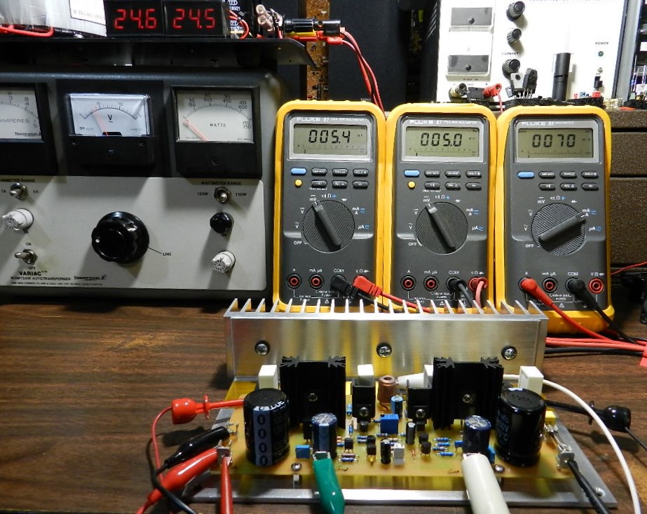
Insert a piece of jumper wire at the input of the amplifier. Do not connect any load or loudspeaker at the output of the amplifier. Prepare 3 DMMs to measure the DC offset voltage, the voltage between the emitters of Q18 and Q22 power output transistors and the current across the F+ fuse terminals.
The picture on the left with a ±24VDC power supply shows the DC offset voltage at 5.4mV measured at the output of the amplifier, 5mV across the emitters of Q18 and Q22 and the current measured across the F+ fuse terminals at 70mA. Carefully adjust VR1 to obtain the 5mV reading after a warm-up period of about 10 minutes. If you get different DMM readings, switch the power supply to OFF immediately and check the PCB for assembly errors. If you plan to power the project at this voltage level you may do so, the music fidelity it reproduced, in my opinion, is still very pleasing and does not disappoint!
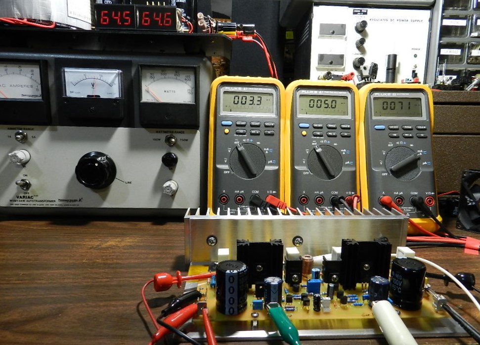
If a Variac transformer is available, connect the AC input of the power supply to the output of the Variac transformer. Switch the power to ON and gradually adjust the Variac’s AC output voltage from zero until the voltage output of the power supply reaches ±64VDC while keeping an eye on sudden increase in any DMM readings. If you have noticed an increase in any of the DMM readings, try adjusting VR1, if not switch the power to OFF immediately and check the PCB for assembly errors. The picture on the right with a ±64VDC power supply shows a DC offset voltage at 3.3mV, the voltage across Q18 and Q22 at 5mV and the current across the F+ fuse terminals at 71mA. Readjust VR1 to get the 5mV reading after 10 minutes, after that, you may proceed with music test!
If a Variac transformer is unavailable, make sure that the power supply has been properly built and that the output voltage rails have been measured at ±64VDC before connecting it to the project. With the power supply at OFF, adjust VR1 for minimum resistance. Switch the power supply to ON; the DMM measuring the voltage across Q18 and Q22 should read less than 1mV. If the DMM reading is more than 1mV and cannot be adjusted by VR1, power OFF immediately and check the PCB for assembly errors. If the DMM reading is less than 1mV wait for 10 minutes for the bias to stabilize and then carefully adjust VR1 to get the 5mV reading, after that, you may proceed with music test!
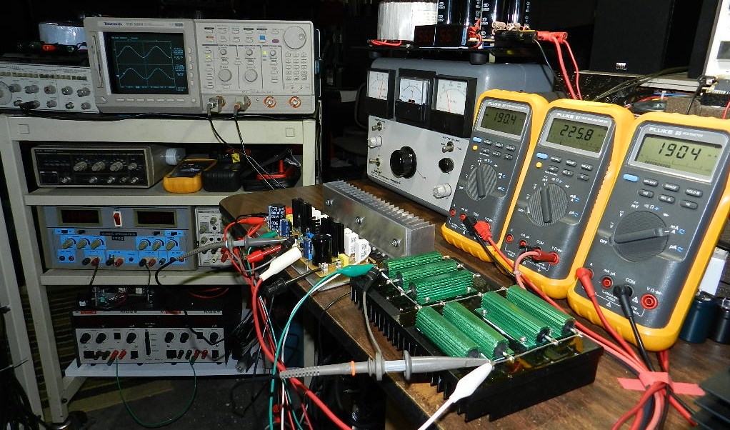
The next test procedure is optional, but if an oscilloscope, audio signal generator and 8Ω dummy load are available, the maximum power output before clipping occurs can be measured. Be careful not to touch the heatsink or the dummy load during this test, they will get very hot. After building Project 21, I’ve improved the dummy load’s heatsink and added more series-parallel connected power resistors for a total resistance of 8Ω and a combined power rating of 700watts, as shown in the picture on the left.
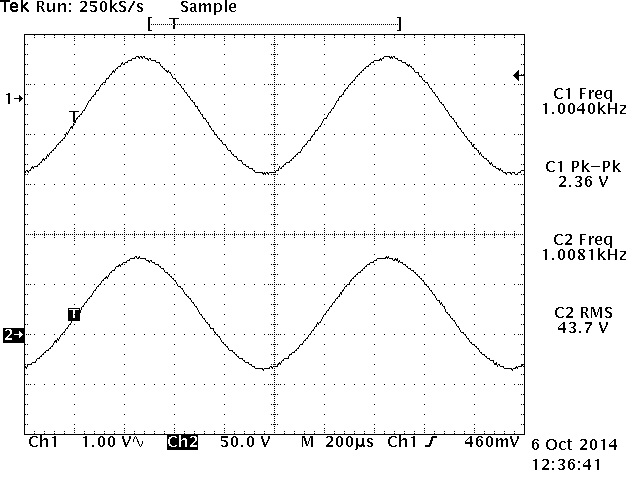
The power output was measured using an HP3312A Function Generator set at 1KHz 2.36Vp-p sine wave output and connected directly to the input of the amplifier under test as well as the CH1 test probe of the oscilloscope. An 8Ω/700Watt dummy load was connected at the output of the amplifier under test as well as the CH2 test probe of the Tektronix TDS520D 500MHz Digital Phosphor Oscilloscope. The amplifier produces 43.7Vrms across the 8Ω/700W dummy load or a power output of about 238Wrms, as shown in the TEK hardcopy picture on the right. The oscilloscope’s horizontal scale was adjusted at 200uS to verify for any visible clipping or artifacts on either peak.
The update should be a worthwhile project if reliability or music fidelity was the major concern. This project was paired with Project 9, the LM1036 tone control project. Enjoy!