Project 64
Project 64 is the 3rd in the series of audio power amplifier projects that uses an Operational Amplifier (op-amp) in the front-end input stage of the amplifier. Currently, there are more than 10 built amplifier projects in this same series. Project 64 is based on the Alexander current feedback amplifier design and the Exicon’s MOSFET high performance amplifier application notes. An op-amp in the input stage is configured as part of the current feedback amplifier. However, instead of driving IGBTs or complementary lateral MOSFETs, it is connected to a quasi-complementary arrangement of vertical power MOSFETs. The quasi-complementary configured power output stage easily produces a power output of more than 200 watts into an 8Ω load with a THD of 0.0023% and a flat frequency response from 20Hz to 20KHz, as measured by a QA400 audio analyzer.
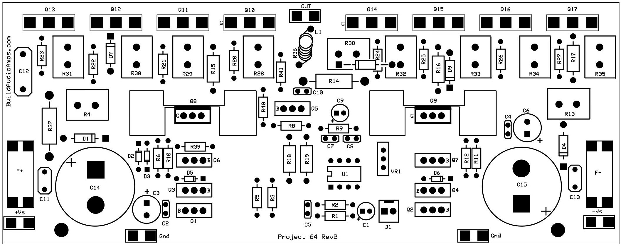
Figure 1. Top silkscreen and bottom copper layer of PCB.
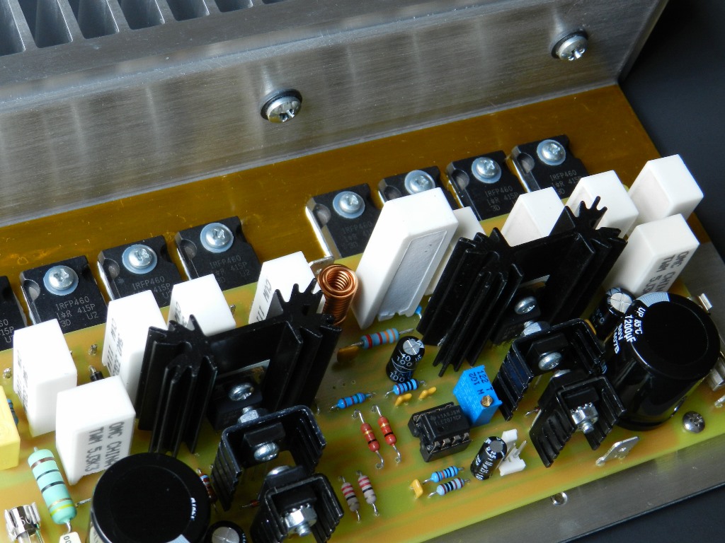
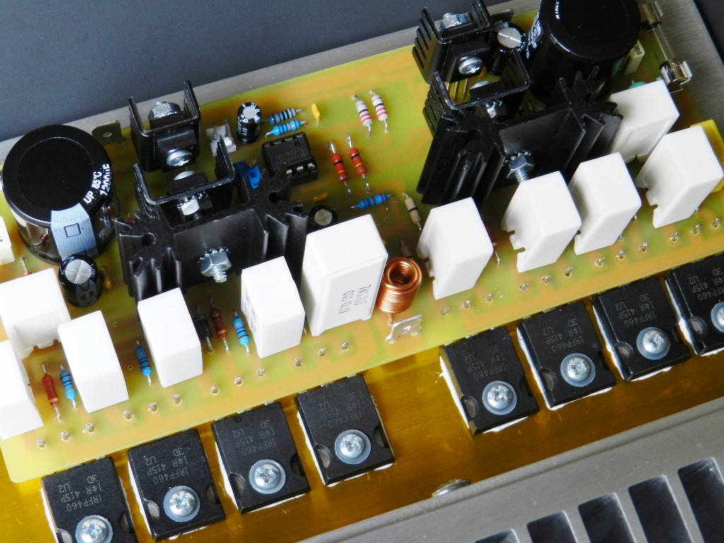
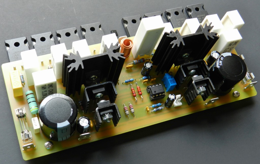
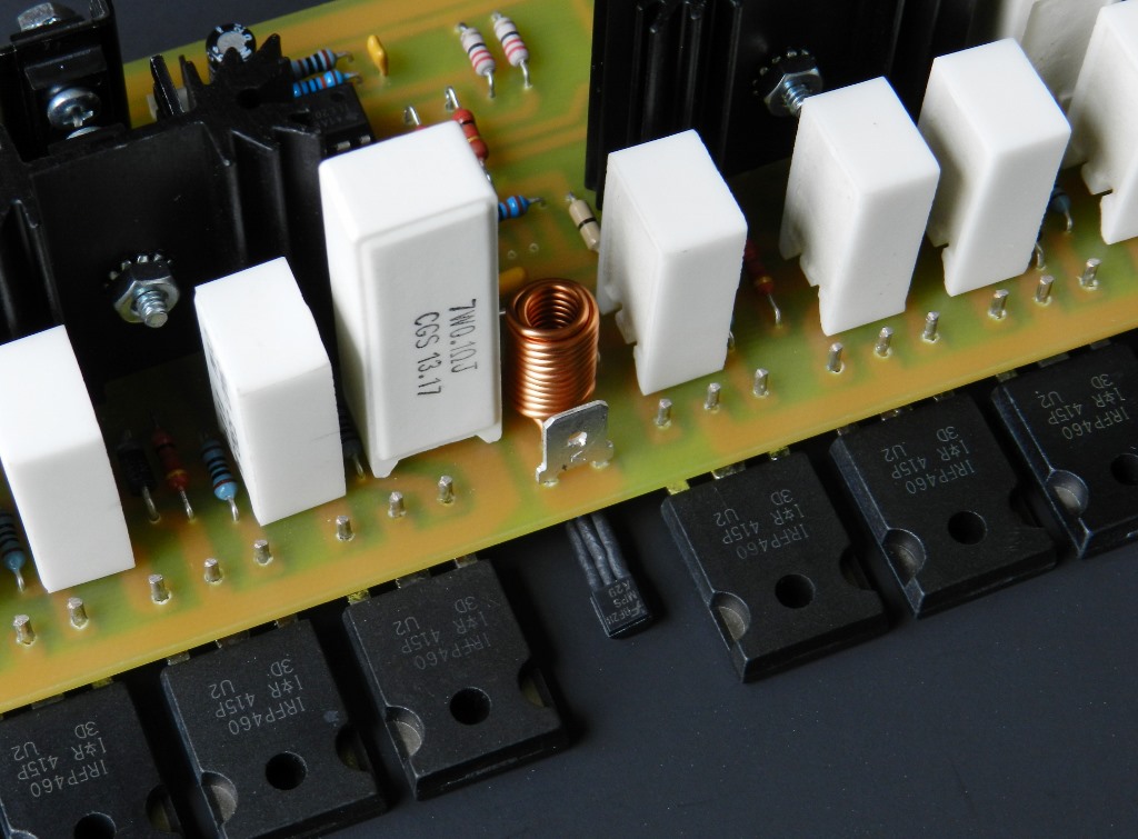
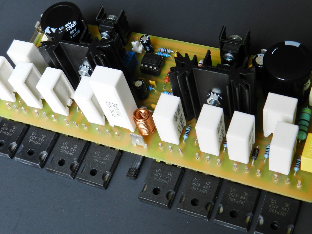
The prototype’s layout was created using ExpressPCB software, laser printed and etched into a 7.00” X 2.75” single-sided printed circuit board as shown in Figures 1. The header and footer pictures on this page will give you an idea of how Project 64 would look like when completed. The PCB layout and BOM are free to registered users and available only by request, as it is, no warranty whatsoever. Please refer to the project’s schematic diagram from hereon.
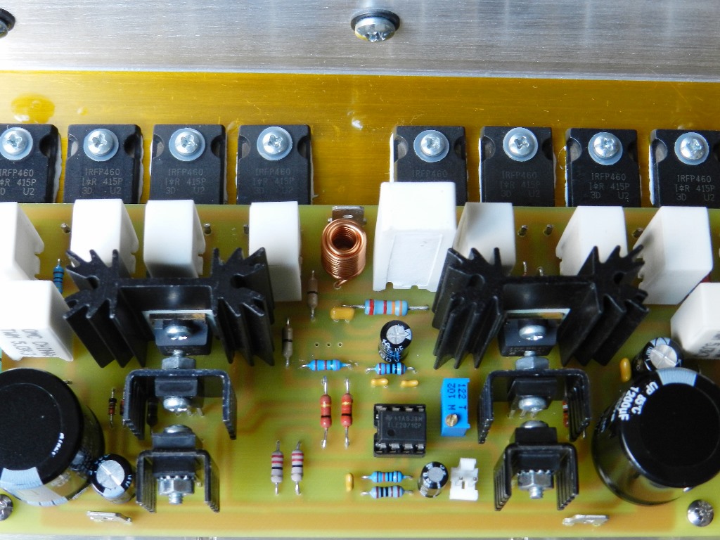
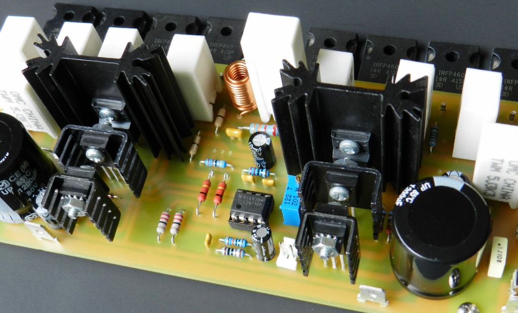
There are a couple of components that are soldered at the bottom copper layer of the PCB as shown in Figure 2. These designated components in the schematic diagram are Q5, D8, VR1 and R7. VR1 and R7 were added, as an afterthought, to adjust the DC offset of the amplifier to minimum or as close to 0mV as possible. At first glance you’ll notice that Q5 is shown in the header pictures as a TO-92 Darlington transistor or as a TO-126 NPN transistor in Figure 2. Both transistor types and packages have been tested and work equally well in the prototype.
The input stage uses a non-inverting JFET-input op-amp, U1, which provide the gain of the amplifier. The output signals are taken from their power supply pins and applied to the emitters of common-base positive and negative voltage regulators, Q1 and Q2. Q1 and Q2 are voltage-referenced at ±15V by D1 and D4. Q1 and Q2 also provide the required dual power supply of the op-amp. The collector outputs of Q1 and Q2 are connected to a common-emitter Q3 and Q4, working as the voltage amplifiers. Q5 and its associated components provide bias to the output stage devices. Q6 and Q7 buffer the input and voltage amplifier stages from the power output stage. The output pin of the op-amp is tied to a low impedance load as well as the frequency-compensation capacitors, C7 and C8. The negative feedback resistors, R3, R5, R18 and R19 determine the gain of the amplifier at 25.7 or 28.2dB. VR1 at pins 1 and 5 of the op-amp adjusts the output DC offset voltage of the amplifier.
The power output stage MOSFETs, Q10 through Q17, have their own source resistor for current sharing and thermal stability. A single drain resistor, R38, has a high-power rating and is connected at the drains of Q14 through Q17. This resistor together with D9 in parallel with R16 improves output stage linearity and assists the lower half CFP-configured MOSFETs emulate as a better complement to the Darlington-configured upper half amplifying MOSFETs. Figures 3, 4, 5 and 6 shows how the 1Vp-p 1KHz sine wave input signal at J1 is amplified at specific test points of interest within the output stage. Figure 3 shows the output waveforms coming from the emitters of Q6 and Q7. These are the signals that go through the gates of Q8 and Q9, respectively. Figure 4 shows the output waveforms from the sources of Q8 and Q9 that goes into the gates of the upper and lower power MOSFETs. As you can see there is no phase inversion but rather a low amplitude signal of 1.6Vp-p at CH2. Interestingly, Figure 5 shows identical output waveforms at the output of the amplifier and drains of the lower half MOSFETs. (Note: The horizontal positions of CH1 and CH2 of the oscilloscope were slightly adjusted apart from each other to show an enhanced viewing of the displayed waveforms.)
There is no protection circuit included within the project, except for the rail fuses, D7 and D8. In reality, it is nearly impossible to completely protect the amplifier against unforeseen device failures, however, the recently updated uPC1237 Speaker Protection and Power ON Delay Project can easily be implemented into the project, for peace of mind.
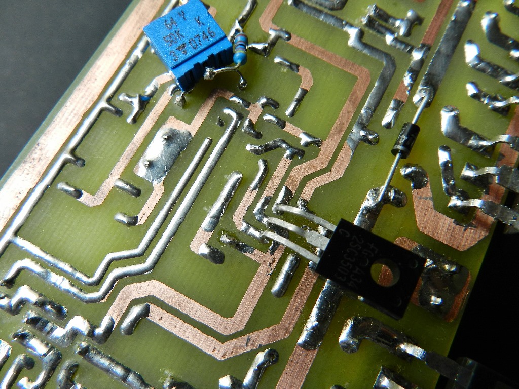
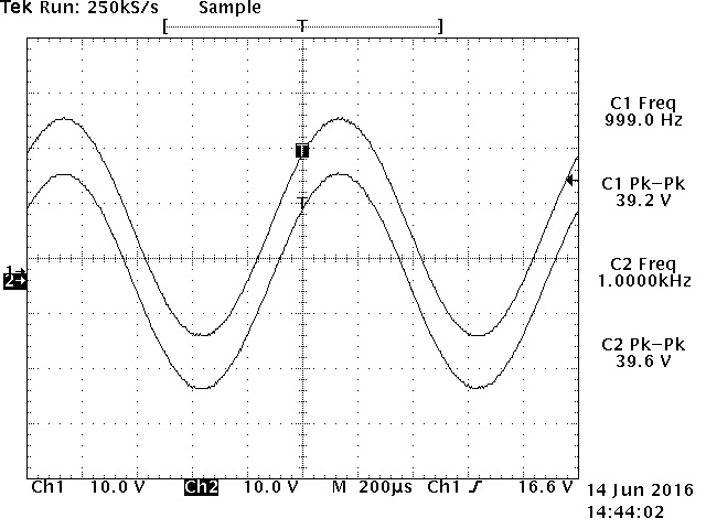
Figure 2. Actual populated bottom copper layer of PCB. Figure 3. CH1 and CH2 at emitters of Q6 and Q7.
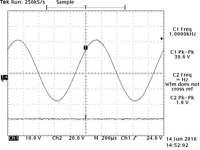
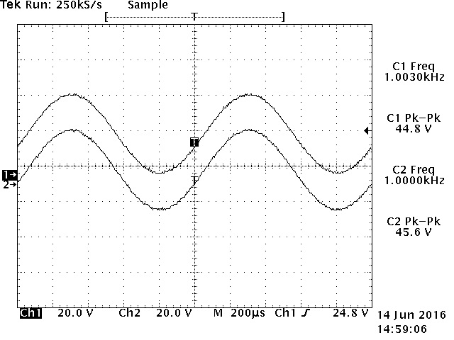
Figure 4. CH1 at gates of upper and CH2 at lower MOSFETs. Figure 5. CH1 at output of amplifier and CH2 at Drain of Lower MOSFETs.
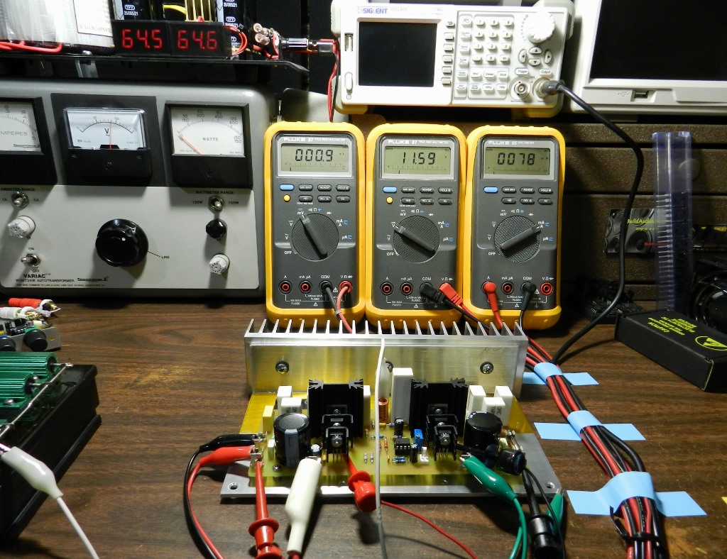
Figure 6. Initial test setup of the Project 64’s prototype.
Before connecting the project’s prototype to the ±64VDC power supply rails, adjust VR2 to maximum resistance at 1KΩ. Do not connect any input signal or load at the output of the amplifier. Figure 6 shows the prototype in its initial test setup and DMM measurements. The DMM on the left is connected at the output of the amplifier. VR1 must be adjusted as close as possible to 0mV, in Figure 6 the DMM measures a DC offset voltage of 0.9mV. The DMM in the middle is connected between the emitter and collector of Q5 and measures a voltage of 11.59V; this was acquired by adjusting VR2 after a warm-up period of about 10 minutes or more. The DMM on the right is connected across the F+ fuse terminals and this measures the total current drawn by the amplifier at 78mA. This reading is dependent on the adjustment of VR2. If you have obtained the same DMM readings you may proceed to the listening test, if not you may perform the next optional tests.
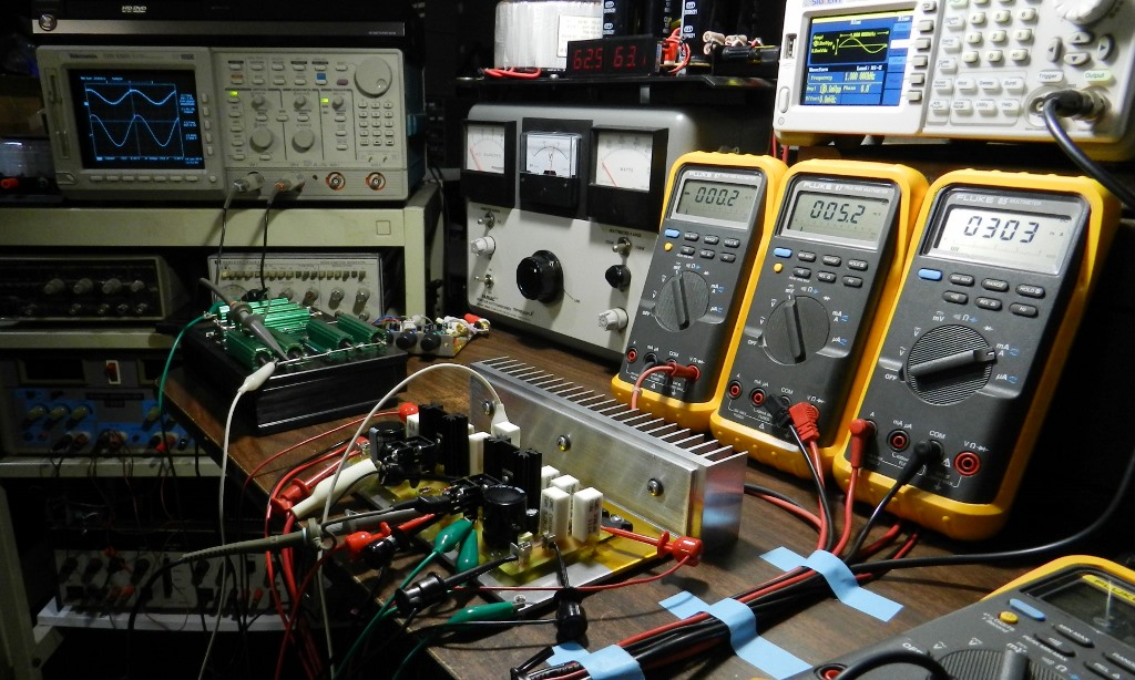
Figure 7. Power output and square wave response test setup of the prototype.
Figure 7 shows the power output and square wave response measurement test setup. The test requires a 2-channel oscilloscope and a signal or function generator. The power output measurement requires a 1KHz sine wave signal adjusted initially at an amplitude of 100mVp-p. This is applied into the input of the amplifier at J1 as well as the CH1 probe of the oscilloscope. An 8Ω dummy load and CH2 probe of the oscilloscope are connected at the output of the amplifier. Slowly adjust the amplitude of the 1KHz sine wave input signal just before clipping occurs as shown in Figure 8a. The prototype produces 40.38Vrms across the 8Ω dummy load; this is equal to the measured power output of 203.8watts. Figure 8b shows a symmetrical clipping when the amplitude of the 1KHz sine wave input signal was adjusted to 2.24Vp-p.

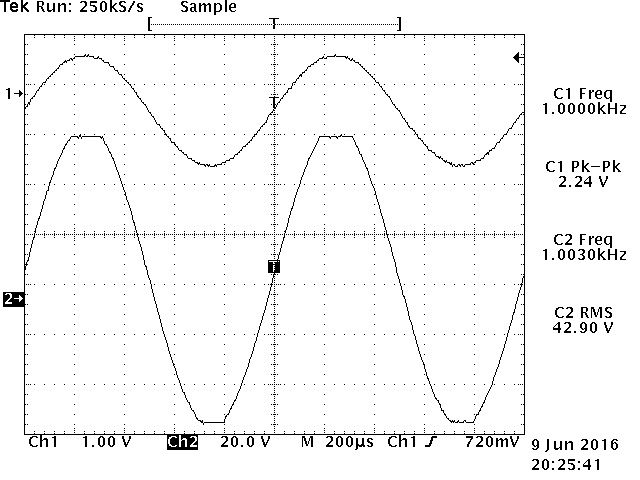
Figure 8a. Power output test result before clipping occurs. Figure 8b. Power output test result with symmetrical clipping.
Figure 9a through Figure 9d shows the 20Hz, 1KHz, 20KHz and 100KHz square wave response test results. The amplitude of the square wave input signal was adjusted just before displaying any signs of overshoots at its peaks. The prototype produces: 110.4Vp-p at 20Hz, 96Vp-p at 1KHz, 58Vp-p at 20KHz and 12.56Vp-p at 100KHz. Be sure to remove R37 when performing the 20KHz and 100KHz square wave response testing.

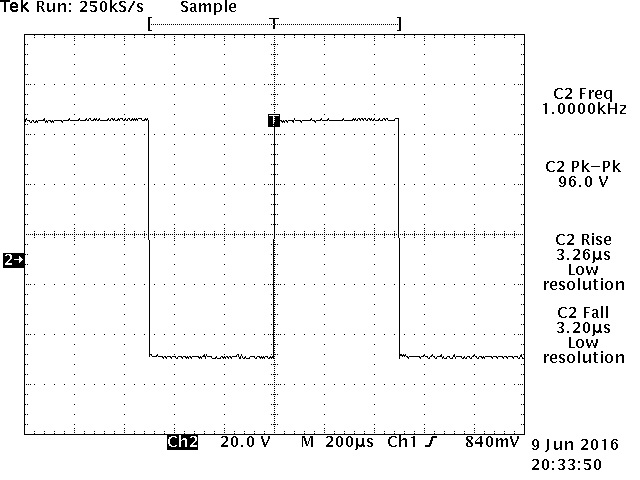
Figure 9a. 20Hz square wave response test result. Figure 9b. 1Hz square wave response test result.
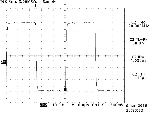
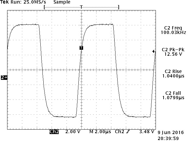
Figure 9c. 20KHz square wave response test result. Figure 9d. 100KHz square wave response test result.
 Figure 10. QA400 audio analyzer test setup.
One of the easiest and most economical ways of measuring THD, Noise, SNR and frequency response with acceptable test results is to use QuantAsylum QA400 USB powered 192Ksps 24-bit stereo audio analyzer with the QA190 differential probe. The QA190 allows you to measure directly the output signal of the audio amplifier and at the same time protects the low-level input of the QA400. Although, QuantAsylum have released their second generation of audio analyzer, but with no foreseeable revenue for the website, the QA400 will suffice at this time to show the measured performance of built audio amplifier projects. Figure 10 shows the QA400 test setup to measure Noise, THD, THD+N, SNR and frequency response. Figure 11a and 11b shows the QA400 audio analyzer test results.
 Figure 11a. Project 64’s Noise, THD, THD+N and SNR test result.
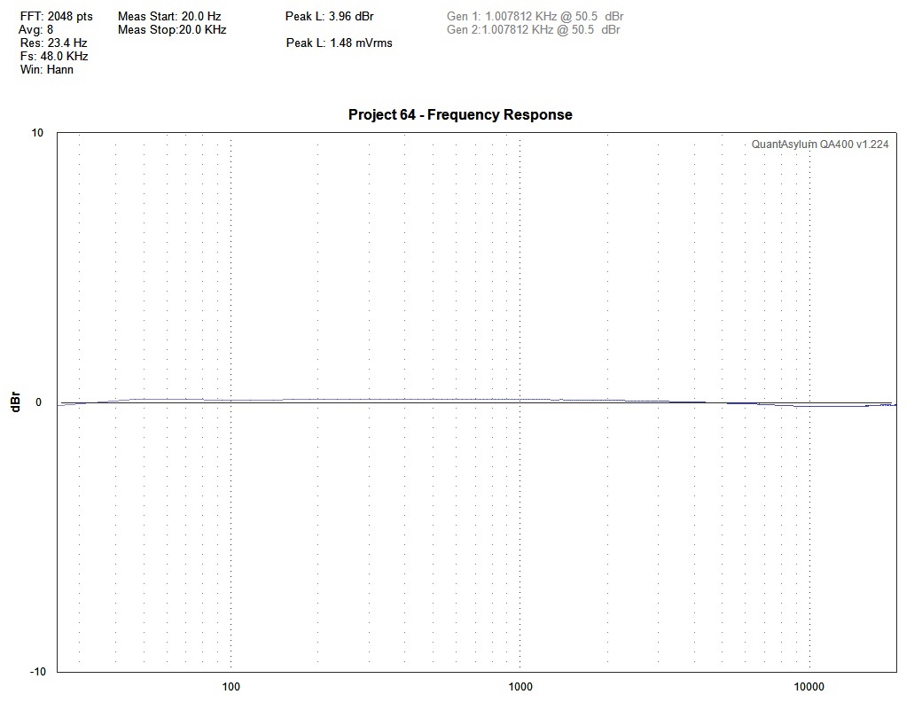
Figure 11b. Project 64’s Frequency Response test result.
How does this project sound? The prototype unit was connected to a modified PreAmp4 tone control preamp, a Toshiba HD-A2 player, several test speakers and finally into a Bose Acoustimass 3 Speaker System with their inputs paralleled. Playing with CD album of different genres, the experience was very impressive and the amplifier sounded powerful.