Project 29
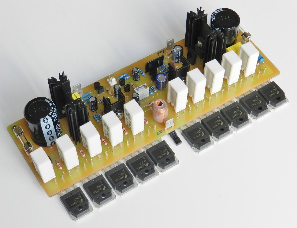
Project 29 features an addition of a cascode circuit at the input stage and a three-stage emitter follower output stage. Project 29 is rated at 218Wrms into an 8Ω load with ±65VDC to ±70VDC power supply rails.
Here’s a brief description of the circuit:
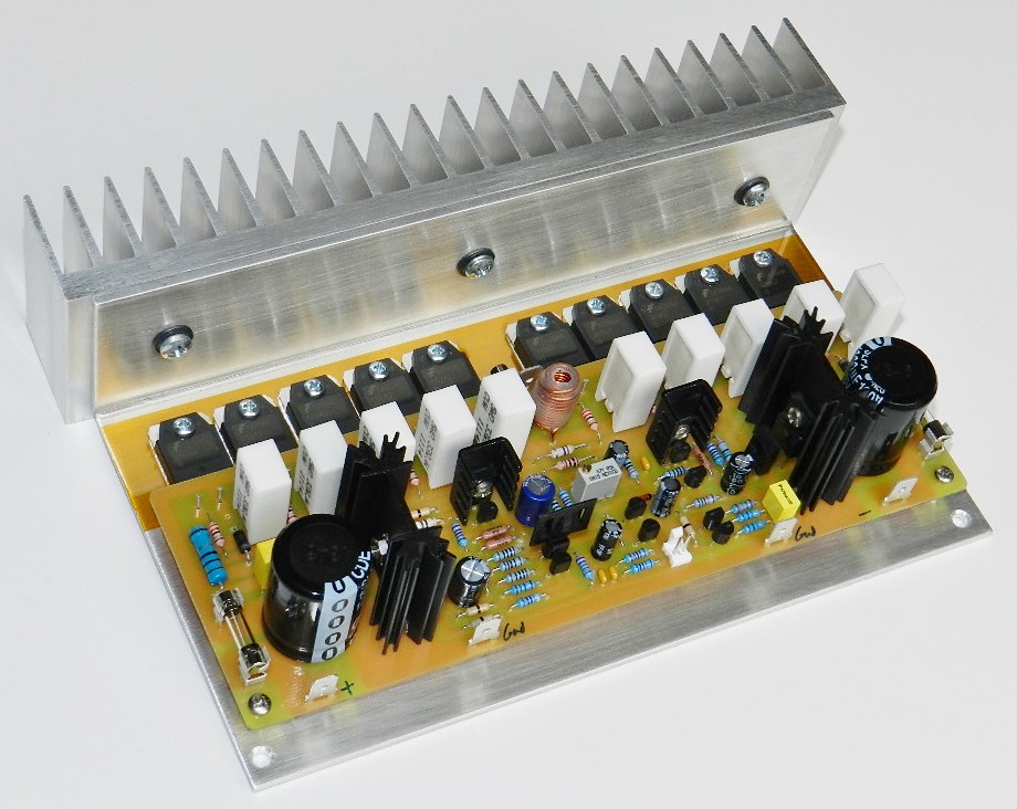
The input signal from J1 passes through a low pass filter that prevents RF noise from entering the base of Q1. The LTP stage is a matched 120V/2A/1W TO-92 transistor pair from Diodes. A heatsink was installed at Q1, as shown in the heading pictures, to compensate for the drift of the DC offset voltage when its case temperature rises with time. With the heatsink installed at Q1, the DC offset voltage never increases to more than 10mV after a warm up period of 15 minutes.
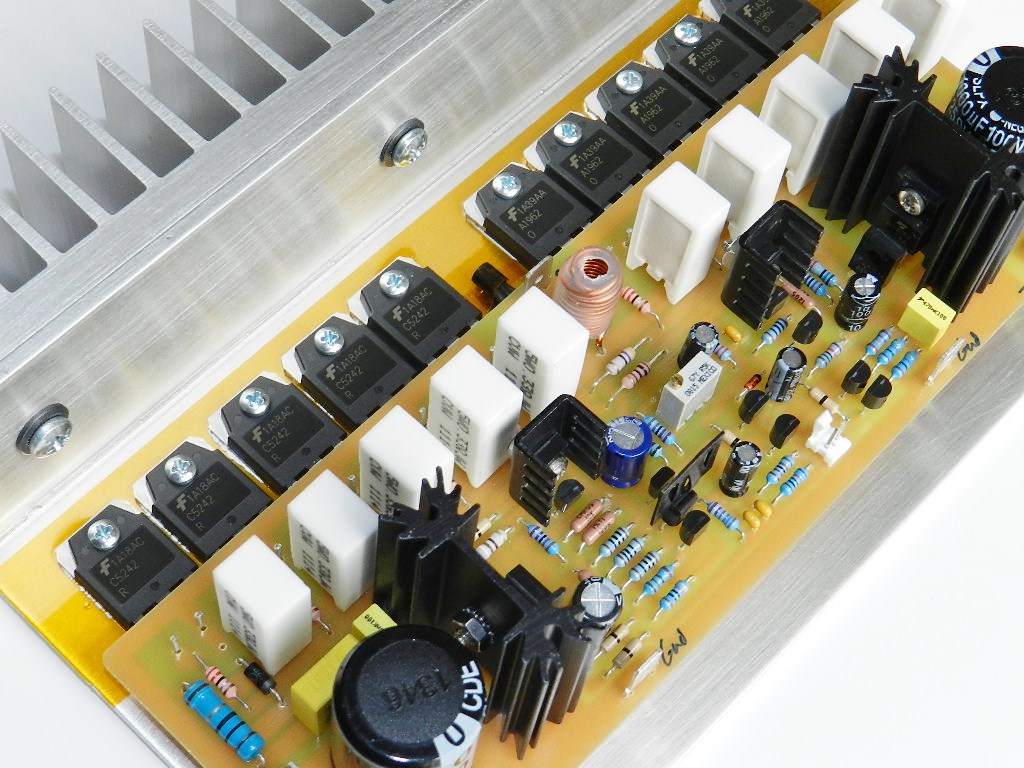
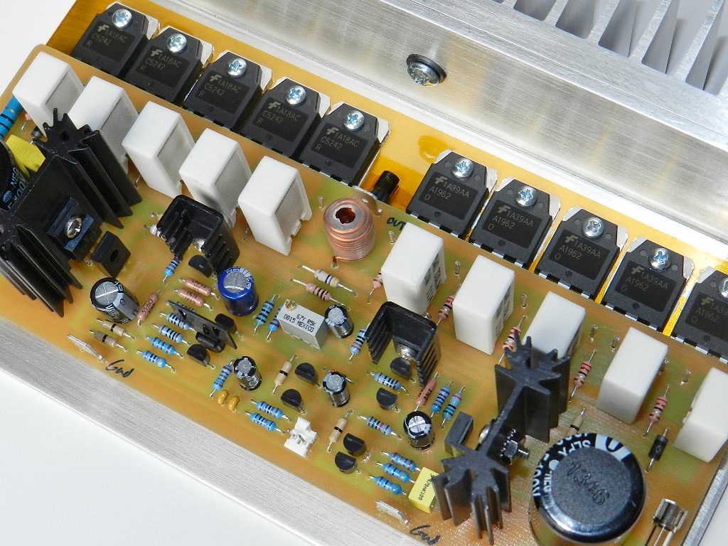
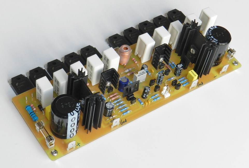
Q1 and Q2 forms as an input differential amplifier, current-sourced by Q3 and their collectors are loaded with current-mirror transistors, Q6 and Q7. Cascode stage transistors, Q4 and Q5, were used in between the output of Q1 and the current mirror circuit to attain wider bandwidth and improve linearity. The output from Q4 is connected to the voltage amplifier stage transistors, Q8, Q10 and Q12, and loaded with current-source transistors, Q9 and Q11. C7 compensates for high frequency instability. The bias of the output stage transistors is set by Q13 and made adjustable by a multi-turn potentiometer VR1. The output stage is a three-stage emitter follower configuration consisting of transistors Q14 through Q27. Pre driver transistors, Q14 and Q15, provide some current gain and isolate the VAS from the main driver stage. Five pairs of complementary 17A, 250V and 130W TO3P package power transistors were used to provide high current when driving low-impedance loads.
If you are interested in building this project and have read the Information and Policies section of this website, the schematic diagram, PCB layout (available only by request) and BOM are free, as is, no warranty.
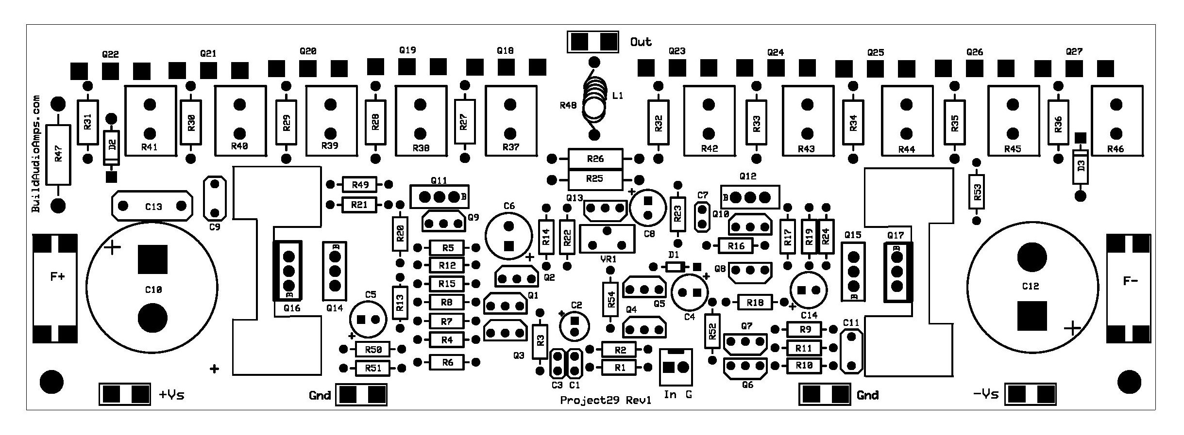
Project 29 Silkscreen parts placement layer of PCB.
A safe way of powering up your newly built project the very first time is to use a low-voltage dual-polarity power supply that you may already have. I’ll be using a ±24VDC power supply for initial testing of the project. The model unit was auditioned with the LM1036 tone control Project 9, a ±5VDC@6A power supply rails and a 3Ω loudspeaker; the sound quality it reproduced at such a very low voltage was surprisingly good and did not disappoint!

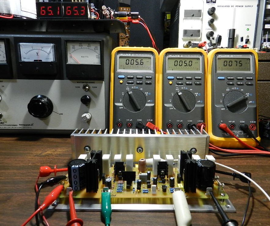
Insert a jumper or shunt at the input of the amplifier. Do not connect any load or loudspeaker at the output of the amplifier. Prepare 3 DMMs to measure the DC offset voltage, the voltage between the emitters of Q22 and Q27 power output transistors and the current across the F+ fuse terminals. Experienced amp builders have more than 3 DMMs.
The picture on the left with a ±24VDC power supply shows the DC offset voltage at 2.1mV measured at the output of the amplifier, 5mV across the emitters of Q22 and Q27 and the current measured across the F+ fuse terminals at 72mA. Carefully adjust VR1 to obtain the 5mV reading after a warm-up period of about 10 minutes. If you get different DMM readings, switch the power supply to OFF immediately and check the PCB for assembly errors.
If a Variac transformer is available, connect the AC input of the power supply to the output of the Variac transformer. Switch the power to ON and gradually adjust the Variac’s AC output from zero until the voltage output of the power supply reaches ±64VDC while keeping an eye on sudden increase in any DMM readings. If you have observed an increase in any of the DMM readings, try adjusting VR1, if not switch the power to OFF immediately before any populated component vaporizes and check the PCB for assembly errors. The picture on the right with a ±65VDC power supply shows a DC offset voltage at 5.6mV, the voltage across Q22 and Q27 at 5mV and the current across the F+ fuse terminals at 75mA. Readjust VR1 to get the 5mV reading after 10 minutes, after that, you may proceed with music test!
If a Variac transformer is unavailable, make sure that the power supply has been properly built and that the output voltage rails have been measured at ±65VDC before connecting it to the project. With the power supply at OFF, adjust VR1 for minimum resistance. Switch the power supply to ON; the DMM measuring the voltage across Q22 and Q27 should read less than 1mV. If the DMM reading is more than 1mV and cannot be adjusted by VR1, power OFF immediately and check the PCB for assembly errors. If the DMM reading is less than 1mV wait for 10 minutes for the bias to stabilize and then carefully adjust the reading to 5mV, after that, you may proceed with music test!
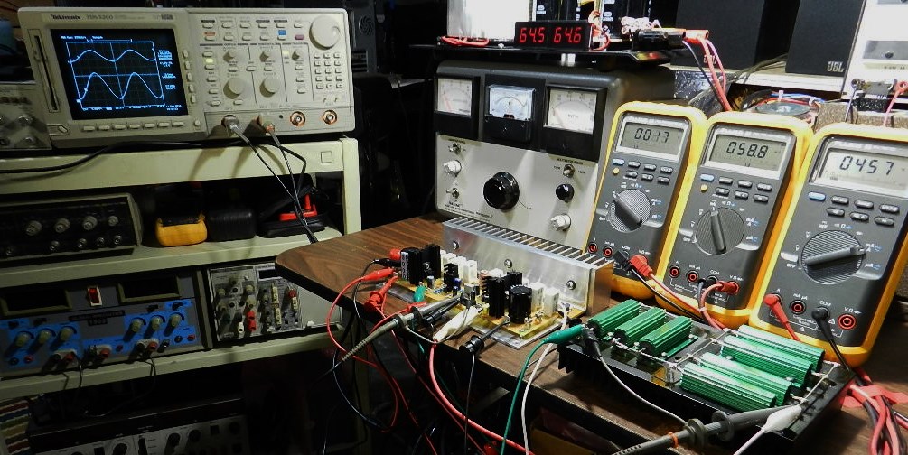
The next test procedure is optional, but if an oscilloscope, audio signal generator and 8Ω dummy load are available, the maximum power output before clipping occurs can be measured. Be careful not to touch the heatsink or the dummy load during this test, they will get very hot.
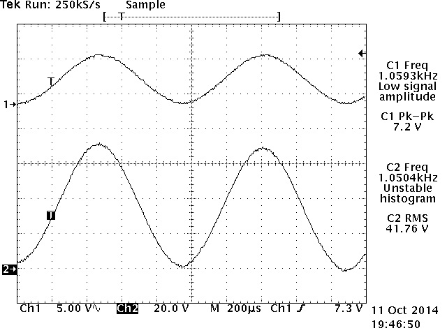
The power output was measured using an HP3312A Function Generator set at 1KHz 7.2Vp-p sine wave output and connected directly to the input of the amplifier under test as well as the CH1 test probe of the oscilloscope. An 8Ω/700Watt dummy load was connected at the output of the amplifier under test as well as the CH2 test probe of the Tektronix TDS520D 500MHz DPO. The amplifier project produces 41.76Vrms across the 8Ω/700W dummy load or a power output of about 218Wrms, as shown in the TEK hardcopy picture on the right. The oscilloscope’s horizontal scale was adjusted at 200uS to verify for any visible clipping or artifacts on either peak. This project was paired with Project 9, the LM1036 tone control project. Enjoy!